

CMOS quad 3-state differential line receiver
Features
■ CMOS design for low power
■ ± 0.2 V sensitivity over input common mode
voltage range
■ Typical propagation delay: 19 ns
■ Typical input hysteresis: 60 mV
■ Input will not load line when V
■ Meets the requirements of EIA standard
RS-422, RS-423
■ 3-state outputs for connection to system buses
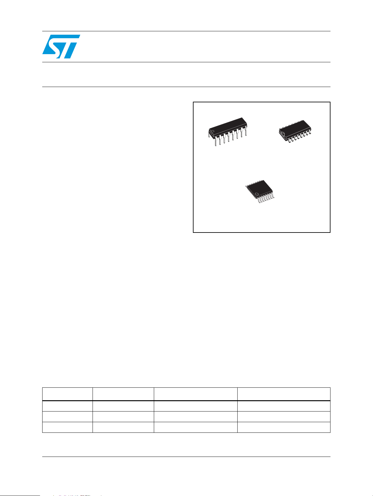
■ Available in surface mount
Description
The ST26C32AB is a quad differential line
receiver designed to meet the RS-422, RS-423
standards for balanced and unbalanced digital
data transmission, while retaining the low power
characteristics of CMOS.
CC
= 0 V
ST26C32AB
DIP-16 SO-16
TSSOP16
The ST26C32AB has an input sensitivity of 200
mV over the common mode input voltage range of
± 7 V. The ST26C32AB features internal pull-up
and pull-down resistors which prevent output
oscillation on unused channels. The ST26C32AB
provides an enable and disable function to all four
receivers and features 3-state output with 6 mA
source and sink capability.
Table 1. Device summary
Order codes Temperature range Package Packaging
ST26C32ABN -40 to 85 °C DIP-16 25 parts per tube / 40 tube per box
ST26C32ABDR -40 to 85 °C SO-16 (tape and reel) 2500 parts per reel
ST26C32ABTR -40 to 85 °C TSSOP16 (tape and reel) 2500 parts per reel
June 2008 Rev 4 1/14
www.st.com
14

Contents ST26C32AB
Contents
1 Pin configuration . . . . . . . . . . . . . . . . . . . . . . . . . . . . . . . . . . . . . . . . . . . . 3
2 Maximum ratings . . . . . . . . . . . . . . . . . . . . . . . . . . . . . . . . . . . . . . . . . . . . 5
3 Electrical characteristics . . . . . . . . . . . . . . . . . . . . . . . . . . . . . . . . . . . . . 6
4 Package mechanical data . . . . . . . . . . . . . . . . . . . . . . . . . . . . . . . . . . . . . 7
5 Revision history . . . . . . . . . . . . . . . . . . . . . . . . . . . . . . . . . . . . . . . . . . . 13
2/14
ST26C32AB Pin configuration
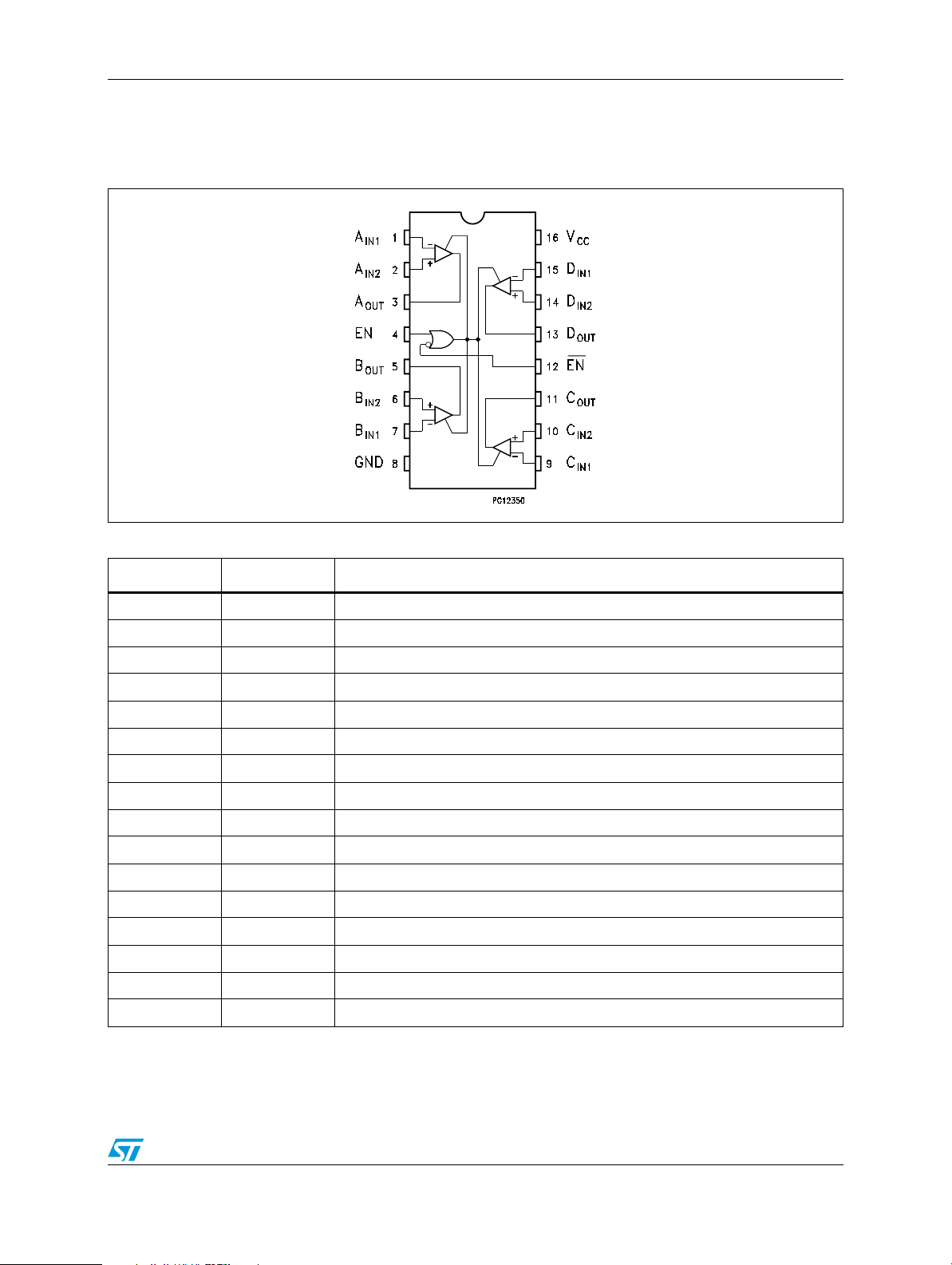
1 Pin configuration
Figure 1. Pin connections
Table 2. Pin description
Pin n° Symbol Name and function
1A
2A
3A
IN1
IN2
OUT
Input A1
Input A2
Channel A Output
4 EN ENABLE
5B
6B
7B
OUT
IN2
IN1
Channel B Output
Input B2
Input B1
8 GND Ground
9C
10 C
11 C
IN1
IN2
OUT
Input C1
Input C2
Channel C output
12 EN ENABLE
13 D
14 D
15 D
16 V
OUT
IN2
IN1
CC
Channel D output
Input D2
Input D1
Supply voltage
3/14
Pin configuration ST26C32AB
Table 3. Truth table
Enable Enable Input Output
LHXZ
All other combinations of enable inputs
≥ V
V
ID
TH(MAX)
V
≤ V
ID
TH(MIN)
H
L
Open H
Note: L = Low voltage state
H = High logic state
X = Don’t care
Z = High impedance
4/14
ST26C32AB Maximum ratings
2 Maximum ratings
Table 4. Absolute maximum ratings
(1) (2)
Symbol Parameter Value Unit
V
V
V
DIFF
V
I
OMAX
T
STG
1. Absolute maximum ratings are those values beyond which the safety of the device cannot be guaranteed. They are not
meant to imply that the device should be operated at these limits. The table of electrical characteristics provide conditions
for actual device operation.
2. Unless otherwise specified, all voltage are referenced to ground. All currents into the device pins are positive; all currents
out of the device pins are negative.
Supply voltage 7 V
CC
Input common mode range ± 14 V
CM
Differential input voltage ± 14 V
Enable input voltage 7 V
IN
Maximum current per output ± 25 mA
Storage temperature range -65 to +150 °C
Table 5. Recommended operating conditions
Symbol Parameter Value Unit
V
T
t
r
Supply voltage 4.5 to 5.5 V
CC
Operating temperature range -40 to +85 °C
A
, t
Maximum enable input rise or fall times 500 ns
f
5/14
 Loading...