

ST ST24E64, ST25E64 User Manual
查询ST24E64EB1TR供应商
SERIALEXTENDED ADDRESSING COMPATIBLE
COMPATIBLEwith I2C EXTENDED
ADDRESSING
TWO WIRE SERIAL INTERFACE,
SUPPORTS400kHz PROTOCOL
1 MILLION ERASE/WRITECYCLES, OVER
the FULL SUPPLYVOLTAGERANGE
40 YEARSDATA RETENTION
SINGLESUPPLYVOLTAGE
– 4.5V to 5.5V for ST24E64 version
– 2.5V to 5.5V for ST25E64 version
WRITECONTROLFEATURE
BYTEand PAGEWRITE (up to 32 BYTES)
BYTE, RANDOM and SEQUENTIALREAD
MODES
SELFTIMED PROGRAMINGCYCLE
AUTOMATIC ADDRESS INCREMENTING
ENHANCEDESD/LATCHUP
PERFORMANCES
WITH I
ST24E64
ST25E64
2
C BUS 64K (8K x 8) EEPROM
PRELIMINARYDATA
8
1
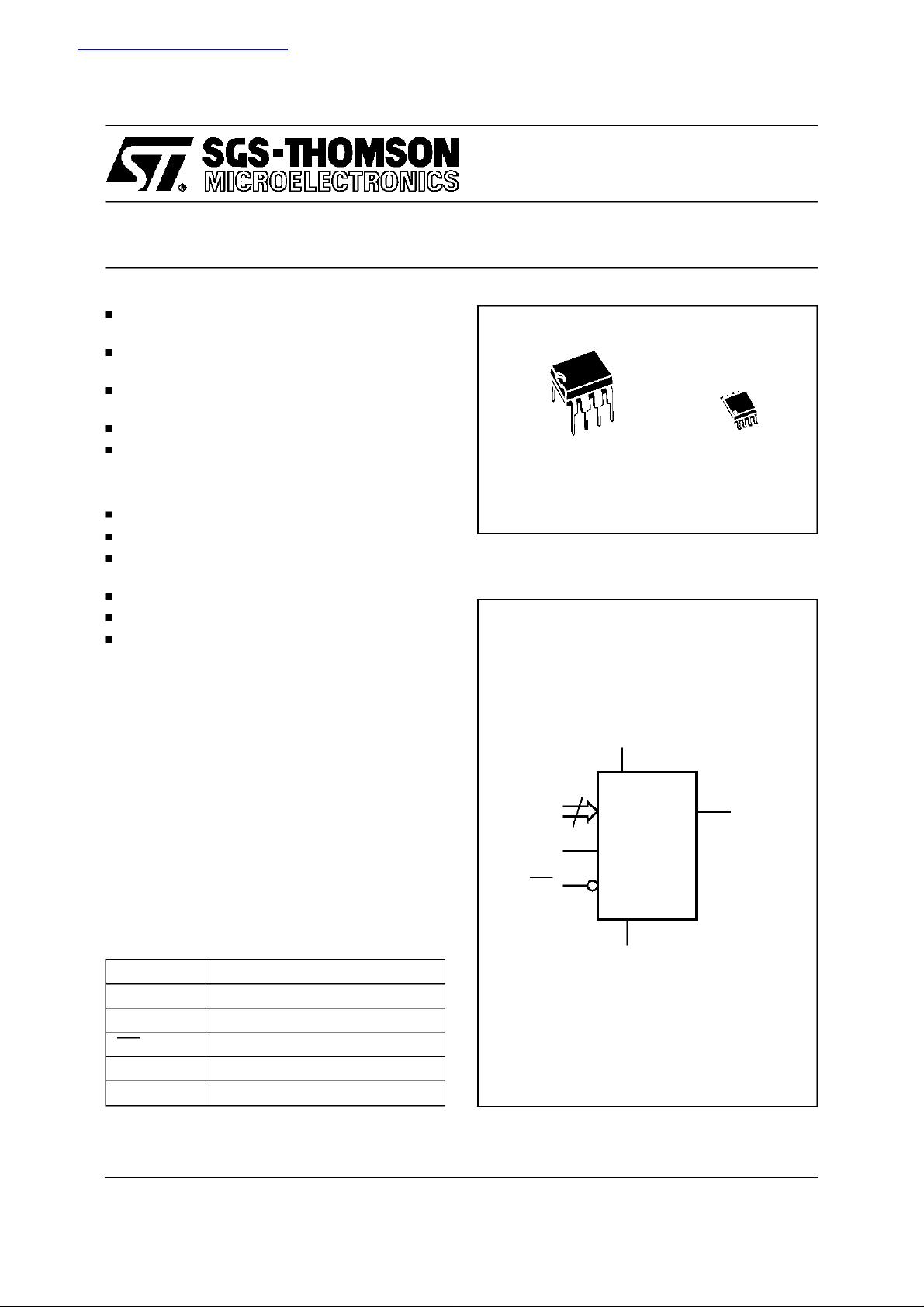
PSDIP8 (B)
0.25mm Frame
Figure 1. Logic Diagram
8
1
SO8 (M)
200mil Width
V
CC
DESCRIPTION
The ST24/25E64 are 64K bit electrically erasable
programmable memories (EEPROM), organized
as8 blocksof 1024x 8bits.TheST25E64operates
with a power supply value as low as 2.5V. Both
PlasticDual-in-LineandPlasticSmallOutlinepack-
E0-E2 SDA
SCL
3
ST24E64
ST25E64
ages are available.
WC
Table 1. Signal Names
V
E0 - E2 Chip Enable Inputs
SDA Serial Data Address Input/Output
SCL Serial Clock
WC Write Control
V
CC
V
SS
November 1996 1/16
This is preliminary information on a newproduct now in development or undergoing evaluation.Details are subject to change without notice.
Supply Voltage
Ground
SS
AI01204B

ST24E64, ST25E64
Figure2A. DIP Pin Connections
ST24E64
ST25E64
E0 V
1
2
E2
3
4
SS
Table2. Absolute MaximumRatings
Symbol Parameter Value Unit
T
A
T
STG
Ambient Operating Temperature –40 to 125 °C
Storage Temperature –65 to 150 °C
8
7
6
5
AI01205B
CC
WCE1
SCL
SDAV
(1)
Figure2B. SO Pin Connections
ST24E64
ST25E64
E0 V
1
2
E2
SS
3
4
8
7
6
5 SDAV
AI01206C
CC
WCE1
SCL
T
LEAD
V
IO
V
CC
V
ESD
Notes: 1. Except for the rating ”Operating Temperature Range”, stresses above those listed in the Table”Absolute Maximum Ratings”
may cause permanent damage to the device. Theseare stress ratings only and operation of the device atthese or any other
conditions above thoseindicated in the Operating sections of this specification is not implied. Exposure to Absolute Maximum
Rating conditions for extended periods may affectdevice reliability. Refer also to the SGS-THOMSON SURE Program and
other relevantquality documents.
2. 100pF through 1500Ω; MIL-STD-883C, 3015.7
3. 200pF through 0Ω; EIAJ IC-121 (condition C)
Lead Temperature, Soldering (SO8)
Input or Output Voltages –0.6 to 6.5 V
Supply Voltage –0.3 to 6.5 V
Electrostatic Discharge Voltage (Human Body model)
Electrostatic Discharge Voltage (Machine model)
(PSDIP8)
(3)
DESCRIPTION (cont’d) slave devices in the I
2
Each memory is compatible with the I
Cextended
addressing standard, two wire serial interface
which uses a bi-directional data bus and serial
clock.TheST24/25E64carrya built-in4bit, unique
deviceidentification code(1010) correspondingto
2
C bus definition.The ST24/25E64behaveas
the I
operationssynchronizedby the serial clock. Read
and write operations are initiated by a START
conditiongeneratedbythebusmaster.TheSTART
conditionis followed by a stream of 4 bits(identification code 1010), 3 bit Chip Enable input to form
a 7 bit DeviceSelect, plus one read/write bit and
terminatedby an acknowledgebit.
40 sec
10 sec
(2)
2
C protocol with all memory
215
260
4000 V
500 V
°C
2/16

ST24E64, ST25E64
Table 3. Device Select Code
Device Code Chip Enable RW
Bit b7 b6 b5 b4 b3 b2 b1 b0
Device Select 1 0 1 0 E2 E1 E0 RW
Note: The MSB b7 is sent first.
Table 4. OperatingModes
Mode RW bit Bytes Initial Sequence
Current Address Read ’1’ 1 START,Device Select, RW = ’1’
Random Address Read
Sequential Read ’1’ 1 to 8192 As CURRENT or RANDOM Mode
Byte Write ’0’ 1 START,Device Select, RW = ’0’
Page Write ’0’ 32 START, Device Select, RW = ’0’
’0’
’1’ reSTART, Device Select, RW = ’1’
1
Whenwritingdata tothememoryit respondsto the
8 bits received by asserting an acknowledge bit
during the 9th bit time. When data is read by the
busmaster,itacknowledgesthereceiptof the data
bytes in the same way.
Data transfers are terminated with a STOP condition. In this way, up to 8 ST24/25E64 may be
connectedto the same I
2
C bus and selected individually, allowing a total addressing field of 512
Kbit.
Power On Reset: V
lock out write protect. In
CC
order to prevent data corruption and inadvertent
write operations during power up, a Power On
Reset(POR) circuit is implemented.Untill the V
CC
voltagehas reachedthe POR thresholdvalue,the
internal reset is active:all operationsare disabled
and the device will not respondto any command.
In the same way, when V
drops down from the
CC
operating voltage to below the POR threshold
value, all operations are disabled and the device
will not respond to any command. A stable V
CC
mustbe appliedbefore applying any logic signal.
START, Device Select, RW = ’0’, Address,
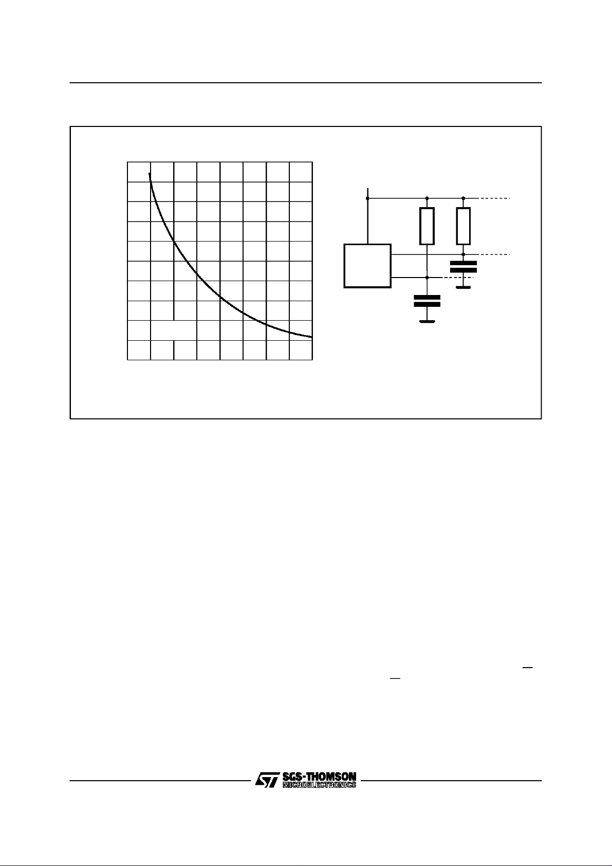
resistorcan be connected fromtheSCLlineto V
to act as a pull up (see Figure 3)
Serial Data (SDA). The SDA pin is bi-directional
and isusedtotransferdatain oroutof the memory.
It is an opendrain output that may be wire-OR’ed
with other open drain or open collector signals on
the bus.AresistormustbeconnectedfromtheSDA
bus line to V
to act as pull up (seeFigure 3).
CC
Chip Enable (E0 - E2). These chip enableinputs
are used to set the 3 least significant bits of the 7
bit deviceselectcode.Theymaybedrivendynamically or tied to V
selectcode. Note that theV
or VSSto establish the device
CC
IL
inputs are CMOS, not TTL compatible.
Write Control (WC). The Write Control feature
WC isuseful to protectthe contentsof the memory
from any erroneous erase/write cycle. The Write
Control signal is used to enable (WC at V
disable (WC at V
) the internal write protection.
IL
When pin WC is unconnected, the WC input is
internallyread as V
(seeTable 5).
IL
When WC = ’1’, Device Select and Addressbytes
are acknowledged; Data bytes are not acknow-
SIGNALSDESCRIPTION
Serial Clock (SCL). The SCLinput pin is used to
synchronize all data in and out of the memory. A
ledged.
Refer to the AN404 ApplicationNote for morede-
tailed information about WriteControl feature.
CC
and VIHlevelsfor the
)or
IH
3/16
ST24E64, ST25E64
Figure3. Maximum RLValueversusBus Capacitance(C
20
16
12
max (kΩ)
L
R
8
4
0
VCC=5V
25 50 75 100
C
(pF)
BUS
) foran I2C Bus, fC= 400kHz
BUS
V
CC
R
L
SDA
MASTER
SCL
C
BUS
R
L
C
BUS
AI01115
DEVICE OPERATION
2
I
C Bus Background
TheST24/25E64supportthe extendedaddressing
2
I
C protocol.This protocol defines any devicethat
sends data onto the bus as a transmitterand any
devicethatreadsthedataas areceiver. Thedevice
that controls the data transfer is known as the
masterand the other as the slave. The masterwill
always initiate a data transfer and will provide the
serial clock for synchronisation. The ST24/25E64
arealways slavedevices in allcommunications.
Start Condition. STARTis identified by a high to
low transition of the SDA line while the clock SCL
isstable in the high state. ASTARTcondition must
precede any command for data transfer. Except
duringa programmingcycle,the ST24/25E64continuously monitor the SDA and SCL signals for a
START conditionand will not respond unless one
isgiven.
StopCondition. STOPisidentifiedbyalowtohigh
transition of the SDA line while the clock SCL is
stable in the high state. A STOP condition terminates communication between the ST24/25E64
and the bus master.A STOP condition at the end
of a Read command forces the standby state. A
STOP condition at the end of a Write command
triggersthe internalEEPROM write cycle.
Acknowledge Bit (ACK). Anacknowledgesignal
is used to indicate a successfuldata transfer.The
bustransmitter, eithermasteror slave,will release
theSDAbusaftersending8 bits of data.Duringthe
9th clock pulse the receiverpulls the SDAbus low
to acknowledgethe receiptof the 8 bitsofdata.
Data Input. During data input the ST24/25E64
sample the SDA bus signal on the rising edge of
the clock SCL. For correct device operation the
SDAsignal must be stable during the clock low to
high transition and the data must change ONLY
when the SCL lineis low.
Device Selection. To start communication between the bus master and the slave ST24/25E64,
the master must initiate a STARTcondition.The 8
bitssent after a STARTcondition aremadeup ofa
deviceselectof4bitsthatidentifiesthedevicetype,
3 Chip Enable bits and one bit for a READ (RW =
1) or WRITE (RW = 0) operation. There are two
modesboth for read andwrite. Theseare summarisedinTable4 anddescribedhereafter.Acommunicationbetweenthemasterandtheslaveis ended
witha STOP condition.
4/16
ST24E64, ST25E64
Table5. InputParameters
(1)
(TA=25°C, f =400 kHz )
Symbol Parameter Test Condition Min Max Unit
C
IN
C
IN
Z
WCL
Z
WCH
t
LP
Note: 1. Sampled only,not 100% tested.
Input Capacitance (SDA) 8 pF
Input Capacitance (other pins) 6 pF
WC Input Impedance VIN≤ 0.3 V
WC Input Impedance VIN≥ 0.7 V
Low-pass filter input time constant
(SDAand SCL)
CC
CC
520kΩ
500 kΩ
100 ns
Table 6. DC Characteristics
= –40 to 85°C or 0to 70 °C; VCC=4.5V to 5.5Vor 2.5V to 5.5V)
(T
A
Symbol Parameter Test Condition Min Max Unit
I
LI
I
LO
I
CC
Input Leakage Current
(SCL, SDA, E0-E2)
Output LeakageCurrent
Supply Current (ST24 series)
Supply Current (ST25 series) 1 mA
0V ≤ V
0V ≤ V
IN
OUT
≤ V
≤ V
CC
CC
SDAin Hi-Z
f
= 400kHz
C
(Rise/Fall time < 30ns)
±2 µA
±2 µA
2mA
I
I
V
V
V
CC1
CC2
V
V
OL
V
IN=VSS
Supply Current (Standby)
(ST24 series)
V
IN=VSS
V
=5V,fC= 400kHz
CC
V
IN=VSS
Supply Current (Standby)
(ST25 series)
IL
IH
IL
IH
Input Low Voltage (SCL, SDA) –0.3 0.3 V
Input High Voltage (SCL, SDA) 0.7 V
Input Low Voltage (E0-E2, WC) –0.3 0.5 V
Input High Voltage (E0-E2, WC) VCC– 0.5 VCC+1 V
V
IN=VSS
V
= 2.5V,fC= 400kHz
CC
or VCC,
V
=5V
CC
or VCC,
or VCC,
V
= 2.5V
CC
or VCC,
CC
100 µA
300 µA
5 µA
50 µA
CC
V
VCC+1 V
Output Low Voltage IOL= 3mA, VCC= 5V 0.4 V
Output Low Voltage (ST25 series) I
= 2.1mA, VCC= 2.5V 0.4 V
OL
5/16
 Loading...