

ST24FC21, ST24FC21B, ST24F W21
1 Kbit (x8) Dual Mode Serial EEPROM
1 MILLION ERASE/WRITE CYCLES
40 YEARS DATA RETENTION
3.6V to 5.5V or 2.5V to 5.5V SINGLE SUPPLY
VOLT AGE
HARDWARE WRITE CONTROL (ST24LW21
and ST24FW21)
TTL SCHMITT-TRIGGER on VCLK INPUT
100k / 400k Hz COMPATIBILITY with the I2C
BUS BIT TRANSFER RANGE
TWO WIRE SERIAL INTERFACE I2C BUS
COMPATIBLE
I2C PAGE WRITE (up to 8 Bytes)
I2C BYTE, RANDOM and SEQUENTIAL READ
MODES
SELF TIMED PROGRAMMING CYCLE
AUTOMATIC ADDRESS INCREMENTING
ENHANCED ESD/LATCH UP
PERFORMANCES
ERROR RECOVERY MECHANISM
(ST24FC21 and ST24FW21) VESA 2
COMPATIBLE
ST24LC21B, ST24LW21
for VESA PLUG & P LAY
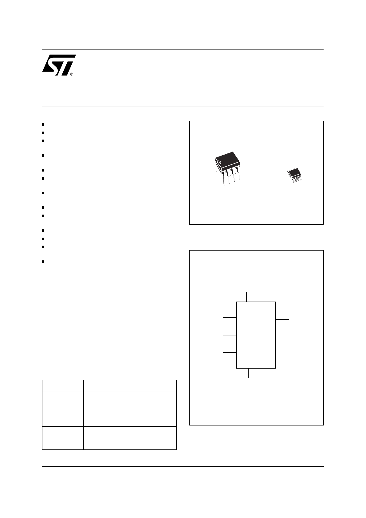
8
1
PSDIP8 (B)
0.25mm Frame
Figure 1. Logic Diagram
8
1
SO8 (M)
150mil Width
V
DESCRIPTION
CC
The ST24LC21B, ST24LW21, ST24FC21,
ST24FC21B and ST24FW21 are 1K bit electrically
erasable programmable memory (EEPROM), organized in 128x8 bits. In the text, products are
SCL
SDA
referred as ST24xy21, where "x" is either "L" for
VESA 1 or "F" for VESA 2 compatible memories
and where "y" indicates the Write Control pin con-
ST24xy21VCLK
nection: "C" means WC on pin 7 and "W" means
WC on pin 3.
WC
Table 1. Signal Names
V
SDA Serial Data Address Input/Output
2
SCL Serial Clock (I
V
CC
V
SS
VCLK Clock Transmit only mode
WC Write Control
June 2002 1/22
Supply Voltage
Ground
C mode)
Note: WC signal is on ly a v a ila b le f o r ST24LW21 and ST24FW21
products.
SS
AI01741
ST24LC21B, ST24LW21, ST24FC21, ST24FC21B, ST24FW21
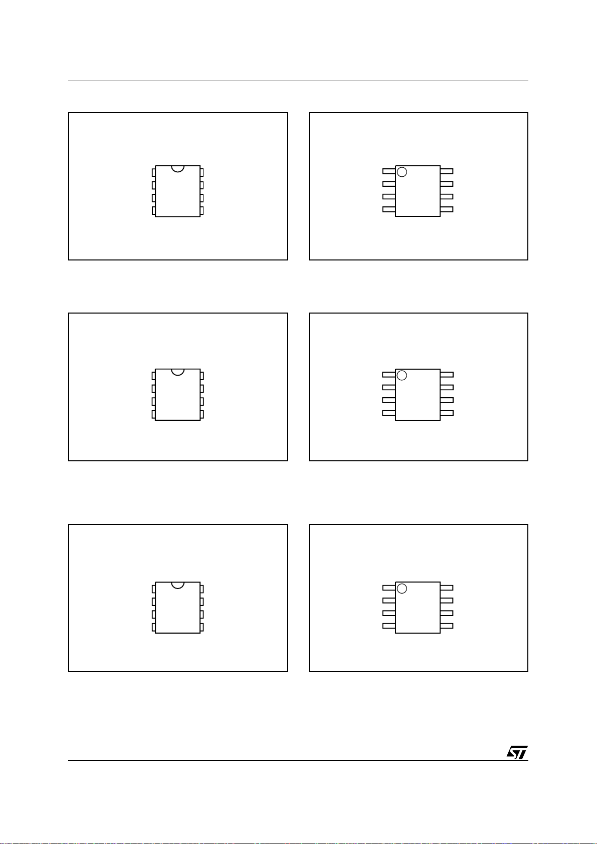
Figure 2A. DIP Pin Connections
ST24LC21B
1
NC V
2
3
NC
4
SS
Warning: NC = Not Connected. Warning: NC = Not Connected.
8
7
6
5
AI01742
CC
VCLKNC
SCL
SDAV
Figure 2C. DIP Pin Connections
ST24FC21
ST24FC21B
1
NC V
2
3
DU
4
SS
8
7
6
5
AI01744
CC
VCLKNC
SCL
SDAV
Figure 2B. SO Pin Connections
ST24LC21B
NC V
1
2
NC
SS
3
4
AI01743
Figure 2D. SO Pin Connections
ST24FC21
ST24FC21B
NC V
DU
SS
1
2
3
4
AI01745
8
CC
7
VCLKNC
6
SCL
5
SDAV
8
CC
7
VCLKNC
6
SCL
5
SDAV
Warning: NC = Not Connected. DU = Don’t Use, must
be left open or connected to V
or VSS.
CC
Figure 2E. DIP Pin Connections
ST24FW21
ST24LW21
1
NC V
2
3
WC
4
SS
Warning: NC = Not Connected. Warning: NC = Not Connected.
2/22
8
7
6
5
AI01746
CC
VCLKNC
SCL
SDAV
Warning: NC = Not Connected. DU = Don’t Use, must
be left open or connected to V
Figure 2F. SO Pin Connections
ST24FW21
ST24LW21
NC V
WC
SS
1
2
3
4
AI01747
or VSS.
CC
8
7
6
5
CC
VCLKNC
SCL
SDAV
ST24LC21B, ST24LW21, ST24FC21, ST24F C21B, ST24FW21
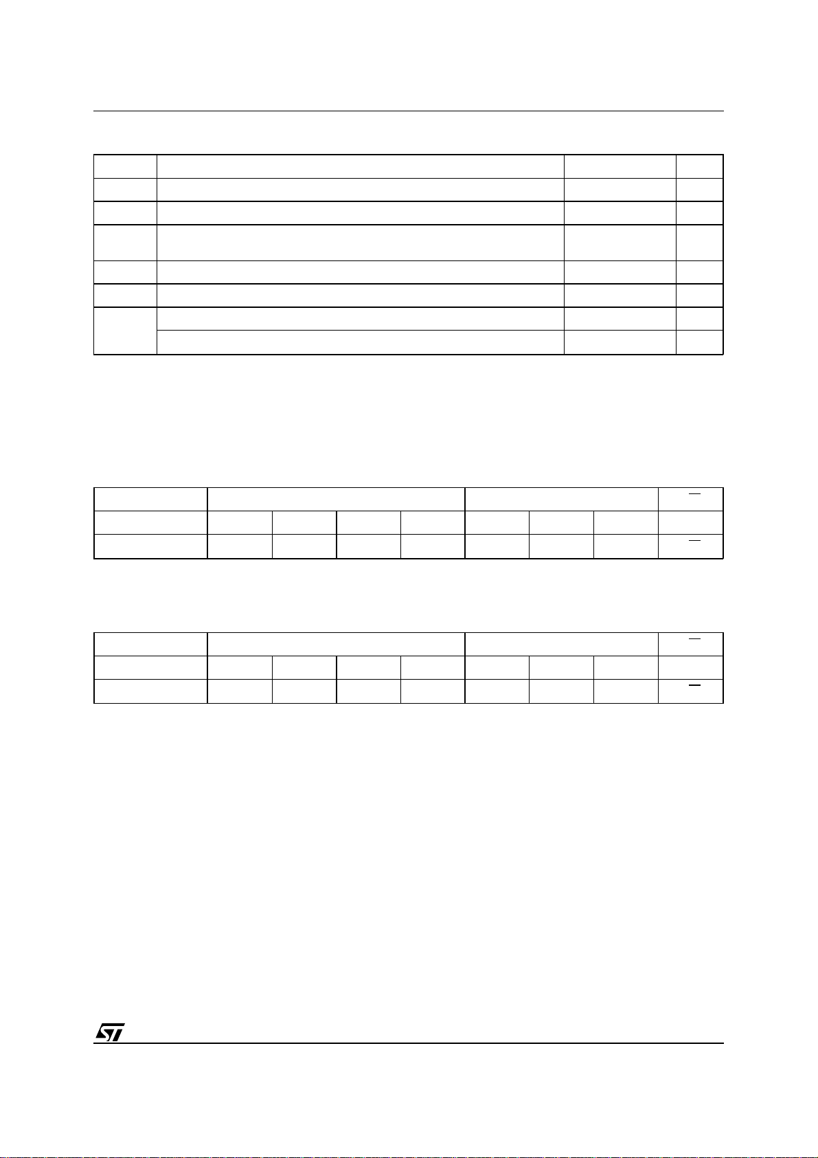
Table 2. Absolute Maximum Ratings
Symbol Parameter Value Unit
T
T
STG
T
LEAD
V
V
V
ESD
Notes: 1. Except for the rating "Operating Temperature Range", stresses above those listed in the Table "Absolute Maximum Ratings"
Ambient Operating Temperature –40 to 85 °C
A
Storage Temperature –65 to 150 °C
Lead Temperature, Soldering (SO8 package)
Input or Output Voltages –0.3 to 6.5 V
IO
Supply Voltage –0.3 to 6.5 V
CC
Electrostatic Discharge Voltage (Human Body model)
Electrostatic Discharge Voltage (Machine model)
may ca use permanent damage to the device. These are stress ratings only and operation of the device at these or any other
conditions above those indicated in the Operating sections of this specification is not implied. Exposure to Absolute Maximum
Rating conditions for extended periods may affect device reliability. Refer also to the STMicroelectronics SURE Program and other
relevant quality docum ent s.
2. MIL-STD-883C, 3015.7 (100pF , 1500 Ω).
3. EIAJ IC-121 (Condition C) (200pF, 0 Ω).
(1)
(PSDIP8 package)
40 sec
10 sec
(2)
(3)
215
260
4000 V
500 V
Table 3A. Device Select Code (ST24LC21B, ST24LW21, ST24FC21 and ST24FW21)
Device Code Chip Enable RW
Bit b7 b6 b5 b4 b3 b2 b1 b0
Device Select 1 0 1 0 X X X R
Note: The MSB b7 is sent first.
X = 0 or 1.
°C
W
Table 3B. Device Select Code (ST24FC21B)
Device Code Chip Enable RW
Bit b7 b6 b5 b4 b3 b2 b1 b0
Device Select 1 010000R
Note: The MSB b7 is sent first.
X = 0 or 1.
DESCRIPTION (cont’d)
The ST24xy21 can operate in two modes: Trans-
mit-Only mode and I
2
C bidirectional mode. When
powered, the device is in Transmit-Only mode with
EEPROM data clocked out from the rising edge of
the signal applied on VCLK.
The device will switch to the I
upon the falling edge of the signal applied on SCL
pin. When in I
2
C mode, the ST24LC21B (or the
2
C bidirectional mode
ST24LW21) cannot switch back to the Transmit
Only mode (except when the power supply is removed). For the ST24FC21, ST24FC21B (or the
ST24FW21), after the falling edge of SCL, the
switch back to the Transmit-Only mode if no valid
2
C activity is observed. Both Plastic Dual-in -Line
I
and Plastic Small Outline packages are available.
Transmit Only Mode
After a Power-up, the ST24xy21 is in the Tra nsmit
Only mode. A proper initialization sequence (see
Figure 3) must supply nine clock pulses on the
VCLK pin (in order to internally synchronize the
device). During this initialization sequence, the
SDA pin is in high im pedance. On the rising edge
of the tenth pulse applied on VCLK pin, the device
will output the first bit of byte located at address 00h
(most significant bit first).
W
memory enter in a transition state which allowed to
3/22
ST24LC21B, ST24LW21, ST24FC21, ST24FC21B, ST24FW21
Figure 3. Transmit Only Mode Waveforms
V
CC
SCL
SDA
VCLK
V
CC
SCL
SDA
VCLK
Bit 7
tVPU
12 891011
Bit 6 Bit 4 Bit 0
Bit 5
12 13 17 18 19 20
Bit 7
Bit 6
Bit 6
AI01501
T able 4. I2C Operating Modes
R
W
Mode
bit
ST24FC21
ST24FC21B
VCLK
ST24LC21B
Current Address
Read
Random Address
Read
’1’ X X 1 START, Device Select, R
’0’ X X
’1’ X X reSTART, Device Select, R
Sequential Read ’1’ X X 1 to 128 Similar to Current or Random Mode
Byte Write ’0’ V
Page Write ’0’ V
Note: X = VIH or V
IL
IH
IH
4/22
ST24LW21
ST24FW21WCBytes Initial Sequence
W = ’1’
START, Device Select, RW = ’0’, Address,
1
W = ’1’
V
IH
V
IH
1 START, Device Select, RW = ’0’
8 START, Device Select, RW = ’0’
ST24LC21B, ST24LW21, ST24FC21, ST24F C21B, ST24FW21
Figure 4. Transition from Transmit Only (DDC1) to Bi-directional (DDC2B) Mode Waveforms
Transmit Only Mode
SCL
SDA
VCLK
- Temporary Bi-Directional Mode
(ST24FC21 and ST24FW21)
- Locked Bi-Directional Mode
(ST24LC21B and ST24LW21)
START
CONDITION
A byte is clocked out (on SDA pin) with nine clock
pulses on VCLK: 8 clock pulses for the data byte
and one extra clock pulse for a Don’t Care bit.
As long as the SCL pin is held high, each byte of
the memory array is transmitted serially on the SDA
pin with an automatic address increment.
When the last byte is transmitted, the address
counter will roll-over to location 00h.
2
C Bidirectional Mode
I
The ST24xy21 can be switched from T ransmit Only
mode to I
2
C Bidirectional mode by applying a valid
high to low transition on the SCL pin (see Figure 4).
– When the ST24LC21B (or the ST24FC21 or
the ST24FC21B) is in the I
2
C Bidirectional
mode, the VCLK input (pin 7) enables (or inhibits) the execution of any write instruction: if
VCLK = 1, write instructions are executed; if
VCLK = 0, write instructions are not executed.
– When the ST24LW 21 (or the ST24FW21) is in
2
C Bidirectional mode, the Write Control
the I
(WC on pin 3) input enables (or inhibits) the
execution of any write instruction: if WC = 1,
write instructions are executed;if WC = 0,
write instructions are not executed.
2
The ST24xy21 is compatible with the I
C standard,
two wire serial interface which uses a bidirectional
data bus and serial clock. The ST24xy21 carries a
built-in 4 bit, unique device identification code
(1010) named Dev ice Select code corresponding
2
to the I
unique device identification code (1010.0000 R
C bus definition. The ST24LC21B carries a
W)
- Locked Bi-Directional
Mode (ST24FC21
and ST24FW21)
1
MSB
2 89
ACK
named Device Select code corresponding to the
2
I
C bus definition.
The ST24xy21 behaves as a slave dev ice in the
2
C protocol with all memory operations synchro-
I
nized by the serial clock SCL. Read and write
operations are initiated by a STAR T condition generated by the bus master. The START condition is
followed by a stream of 7 bits, plus one read/write
bit and terminated by an acknowledge bit.
When data is written into the memory, the
ST24xy21 responds to the 8 bits received by asserting an acknowledge bit during the 9th bit time.
When data is read by the bus master, it must
acknowledge the receipt of the data bytes in the
same way. Data transfers are terminated with a
STOP condition (see READ and WRITE desc riptions in the following pages).
Power On Reset: V
lock out write protect
CC
In order to prevent data corruption and inadvertent
write operations during power up, a Power On
Reset (POR) circuit is implement ed. Until the V
voltage has reached the POR threshold value, the
internal reset is active, all operations are disabled
and the device will not respond to any c ommand.
In the same way, when V
drops down from the
CC
operating voltage to below the POR threshold
value, all operations are disabled and the dev ice
will not respond to any command. A stable V
must be applied before applying any logic signal.
Error Recovery Modes available in the
ST24FC21, ST24FC21B and the ST24FW21
AI01892
CC
CC
5/22
ST24LC21B, ST24LW21, ST24FC21, ST24FC21B, ST24FW21
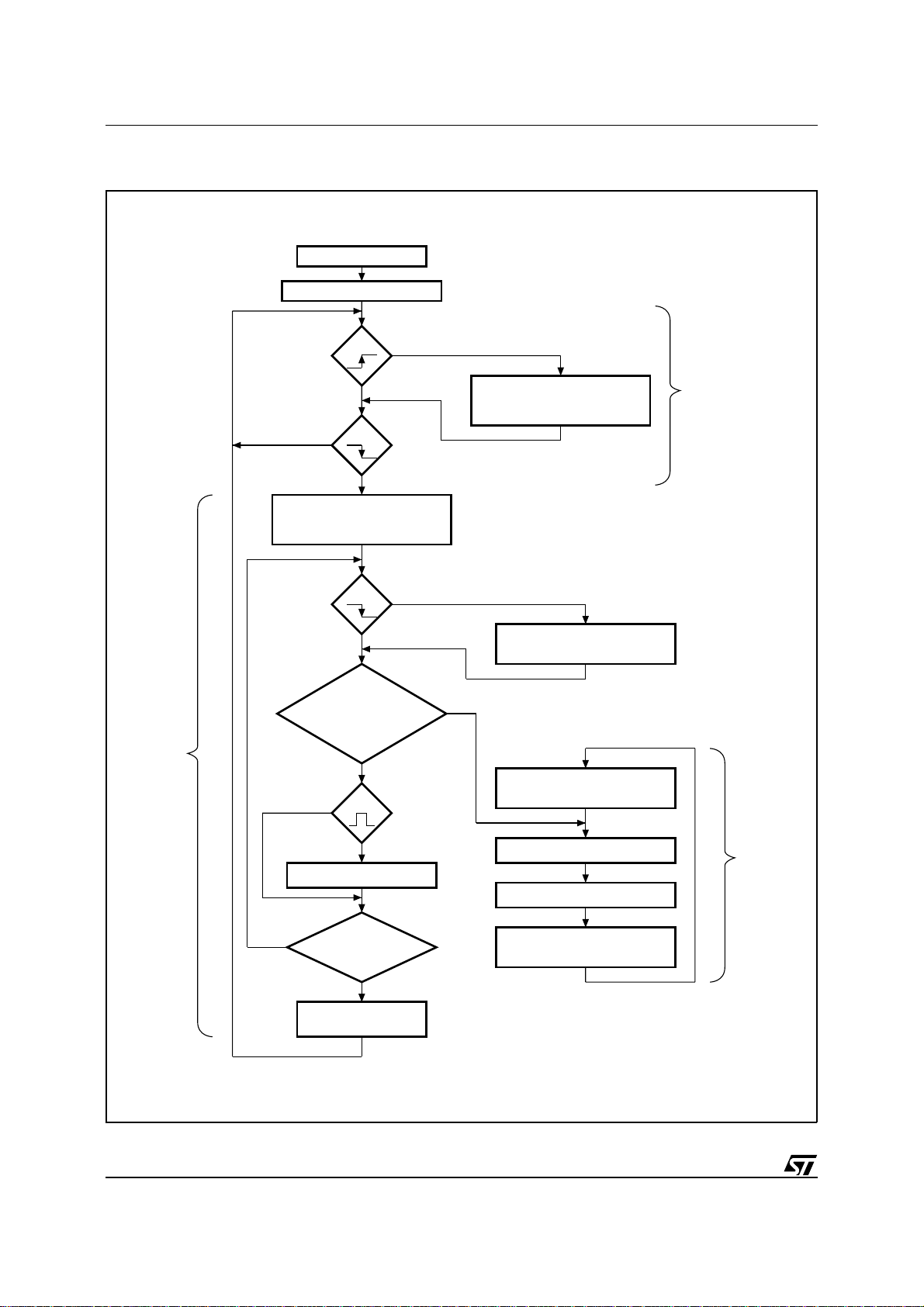
Figure 5. Error Recovery Mechanism Flowchart for the ST24FC21, ST24FC21B and ST24FW21
products
Memory Power On
Internal Address Pointer = 0
Transition
State
(VESA 2)
VCLK
NO
NO
VCLK Internal Counter = 0
Start Internal 2 sec Timer
(START + Device Select)
NO
SCL
SDA Hi-Z
SCL
NO
Valid
2
C access
I
VCLK
YES
YES
YES
?
Send Data bit (MSB first) pointed
by the Address Pointer and
auto-increment pointed bit/byte
Reset VCLK Internal Counter
and Reset Internal Timer
YES
I2C communication idle
waiting for a Device Select byte
Transmit-Only Mode
(DDC1)
6/22
Increment VCLK Counter
NO
Counter = 128
or Timer > 2 sec
Switch Back to
Transmit-Only Mode
YES
YES
Reset Counter and Timer
Send Acknowledge
Respond to the Incoming
2
C Command
I
I2C Mode
(DDC2B)
AI01748
ST24LC21B, ST24LW21, ST24FC21, ST24F C21B, ST24FW21
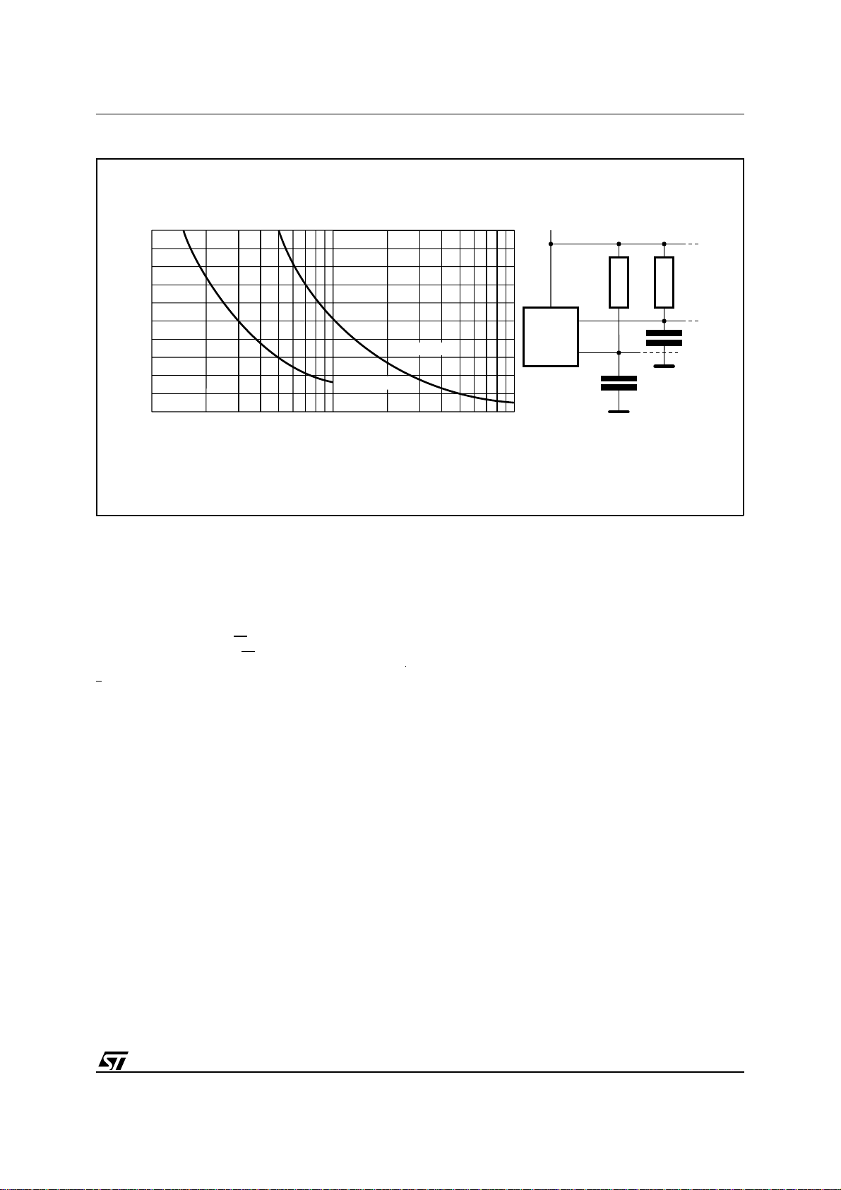
Figure 6. Maximum RL Value versus Bus Capacitance (C
20
16
12
8
Maximum RP value (kΩ)
4
0
10 1000
When the ST24FC21 (or the ST24FC21B or t he
ST24FW21) first switches to the I
DDC2B mode), it enters a transition state which is
functionally identical to I
ST24FC21 (or the ST 24FC21B or the ST24FW21)
does not receive a valid I
2
C operation. But, if the
2
C sequence, that is a
fc = 400kHz
100
C
(pF)
BUS
2
C mode (VESA
ST AR T condition followed by a valid Device Select
code (1010XXX R
ST24FW21; 1010000 R
W for ST24FC21 and
W for ST24FC21B), within
either 128 VCLK periods or a period of time of
t
RECOVERY
(approximately 2 seconds), the
ST24FC21 (or the ST 24FC21B or the ST24FW21)
will revert to the Transmit-Only m ode (VESA DDC1
mode).
If the ST24FC21 (or the ST24FC21B or the
ST24FW21) decodes a valid I
code, it will lock into I
2
C mode. Under this condition,
2
C Device Select
signals applied on the VCLK input will not disturb
READ access from the ST24FC21 (or the
ST24FC21B or the ST24FW21). For WRITE access, refer to the Signal Description paragraph.
When in the transition state, the count of VCLK
pulses and the internal 2 seconds timer are reset
by any activity on the SCL line. This me ans that,
after each high to low transition on SCL, the memory will re-initialise its transition state and will switch
back to Transmit-Only mode only after 128 more
VCLK pulses or after a new t
RECOVERY
delay.
fc = 100kHz
I
to synchronize all data in and out of the memory. A
resistor can be connected from the SCL line to V
to act as a pull up (see Figure 6).
Serial Data (SDA). The SDA pin is bi-directional
and is used to transfer data in or out of the memory.
It is an open drain output that may be wire-OR’ed
with other open drain or open collector signals on
the bus. A resistor must be connected from the SDA
bus line to V
Tr ansmit Only Clock (VCLK). The VCLK input pin
is used to synchronize data out when the ST24xy21
is in Transmit Only mode.
For the ST24LC21B and the ST24FC21 or
ST24FC21B Only, the VCLK offers also a Write
Enable (active high) function when the ST24LC21B
and the ST24FC21 or ST24FC21B are in I
rectional mode.
Write Control (WC). An hardware Wri te Control
feature (WC) is offered only on ST24LW21 and
ST24FW21 on pin 3. This feature is usefull to
protect the contents of the memory from any erroneous erase/write cycle. The Write Control signal
is used to enable (WC = V
the internal write protection. When unconnected,
the WC input is internally tied to V
pull-down resistor and the memory is write pro-
2
C Serial Clock (SCL). The SCL input pin is used
tected.
SIGNAL DESCRIPTIONS
DEVICE OPERATION
) for an I2C Bus
BUS
V
MASTER
to act as pull up (see Figure 6).
CC
CC
R
SDA
SCL
) or disable (WC = VIH)
IL
R
L
SS
L
C
BUS
AI01665
by a 100k ohm
C
BUS
2
C bidi-
CC
7/22
 Loading...