

ST2378E
8-bit dual supply 1.71V to 5.5V level translator
General features
■ High speed:
–t
= 15ns (Max.) at TA = 85°C
PD
–V
= 1.8V
L
–V
■ Guaranteed data rate:
–13Mbps (1.8V
■ Low power dissipation:
–I
–I
–I
■ Output impedance:
–|I
–I
■ Bi-directional level translation
■ Totem pole and open drain driving for I
communications
■ 5V tolerant on enable pin
■ Wide operating voltage range:
–V
–VCC(Opr) = 1.71V to 5.5V
■ ESD performance
■ HBM > 15KV ESD protection on I/OV
■ Leadfree Flip-Chip and TSSOP packages
= 5.5V
CC
≤ V
≤ VCC ≤ 5.5V)
L
= I
TS-VL
= 100µA (Max.) at TA = 85°C
QVL
= 10µA (Max.) at TA = 85°C
QCC
| = 20µA(Min. ) a t VL=1.8V; V
OHA
= 1.0µA(Min.) at VL=1.8V V
OLA
(Opr) = 1.71V to V
L
= 1µA (Max.) at TA = 85°C
TS-VCC
CC
CC
CC
2
CC
with I/O V
= 5.5V
= 5.5V
C
lines
± 15KV ESD protection
CC
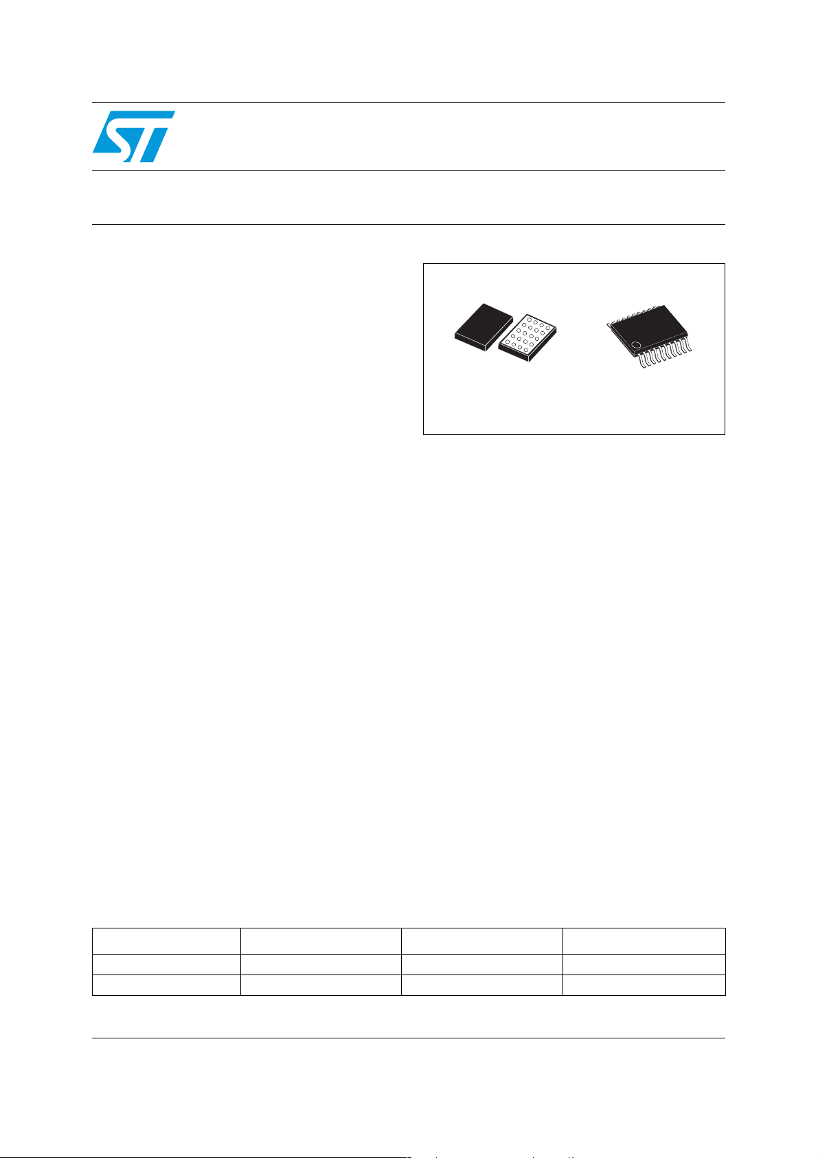
TSSOP20 Flip-Chip20
Description
The ST2378E is an 8-bit, dual supply,
bi-directional level translator with ±15kV ESDprotection on I/Os at V
interface data transfer between low-voltage
ASICs/PLDs and higher voltage systems.
Externally applied voltage, V
levels at both sides with range specified as
1.71V ≤ V
≤ 5.5V and VL ≤ V
L
proper operation, V
VL.
Utilizing a transmission-gate-based design, this
device allows bi-directional asynchronous data
transfer, which means each channel is allowed to
have either V
to VL or VL to VCC data transfer
CC
direction independently and no direction pin is
required. ST2378E operates at guaranteed data
rate of 13Mbps over the entire specified operating
voltage range.
side. It is designed to
CC
and VL, set logic
CC
≤ 5.5V. For
should be set higher than
CC
CC
Among the other features is included the OE pin
which allows disable-mode operation whereby
current consumption is reduced to less than 1µA.
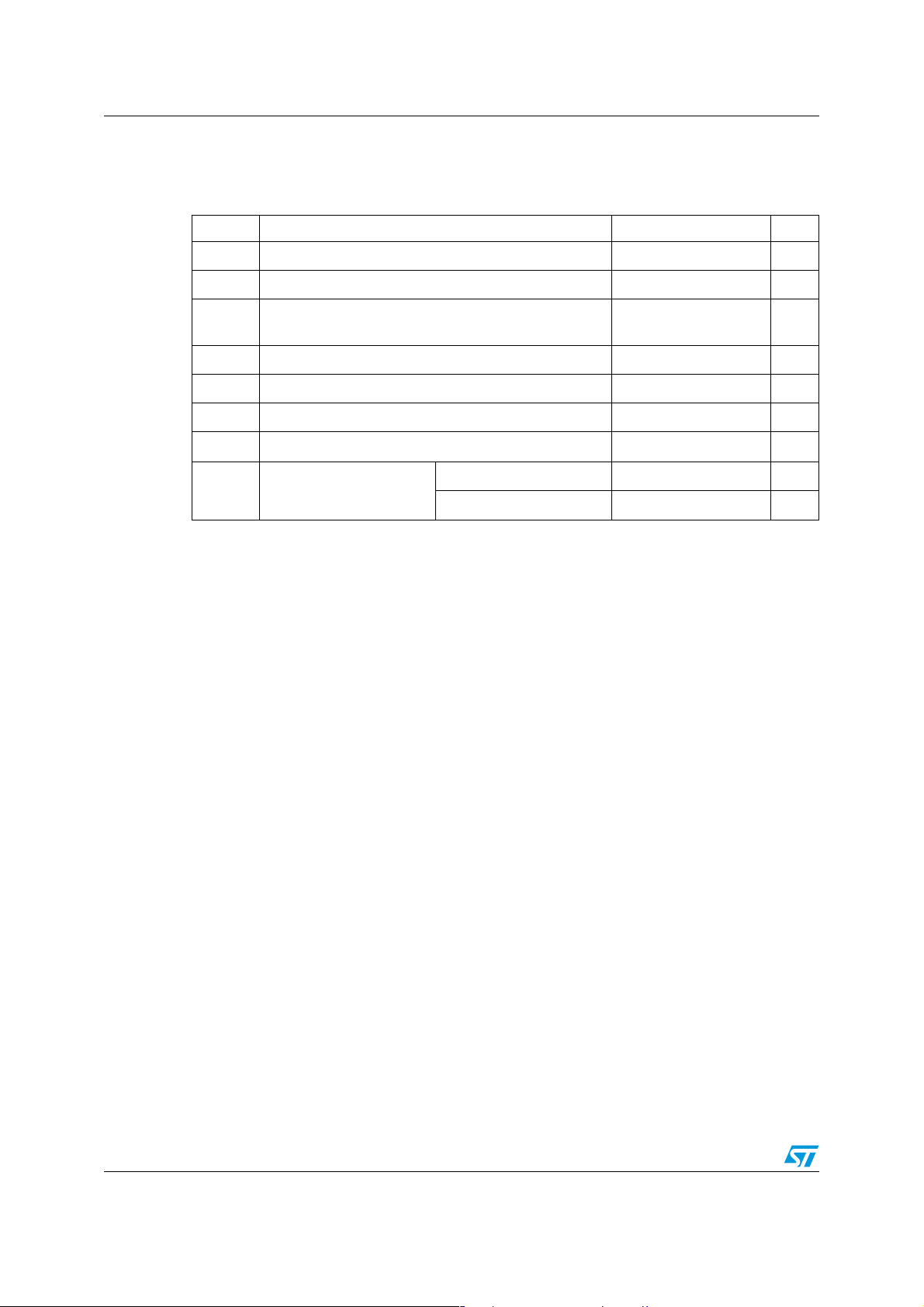
Order codes
Part number Temperature range Package Comments
ST2378EBJR -40 to 85 °C Flip-Chip20 (Tape and Reel) 3000 parts per reel
ST2378ETTR -40 to 85 °C TSSOP20 (Tape and Reel) 2500 parts per reel
April 200 6 Rev 1 1/22
www.st.com
22

Contents ST2378E
Contents
1 Block diagram . . . . . . . . . . . . . . . . . . . . . . . . . . . . . . . . . . . . . . . . . . . . . . 3
2 Pin settings . . . . . . . . . . . . . . . . . . . . . . . . . . . . . . . . . . . . . . . . . . . . . . . . 4
2.1 Pin connection . . . . . . . . . . . . . . . . . . . . . . . . . . . . . . . . . . . . . . . . . . . . . . 4
2.2 Pin description . . . . . . . . . . . . . . . . . . . . . . . . . . . . . . . . . . . . . . . . . . . . . . 4
3 Electrical data . . . . . . . . . . . . . . . . . . . . . . . . . . . . . . . . . . . . . . . . . . . . . . 5
3.1 Maximum ratings . . . . . . . . . . . . . . . . . . . . . . . . . . . . . . . . . . . . . . . . . . . . 5
3.2 Recommended operating conditions . . . . . . . . . . . . . . . . . . . . . . . . . . . . . 5
4 Electrical characteristics . . . . . . . . . . . . . . . . . . . . . . . . . . . . . . . . . . . . . 7
5 Test circuit . . . . . . . . . . . . . . . . . . . . . . . . . . . . . . . . . . . . . . . . . . . . . . . . 13
6 Waveforms . . . . . . . . . . . . . . . . . . . . . . . . . . . . . . . . . . . . . . . . . . . . . . . . 14
7 Mechanical data . . . . . . . . . . . . . . . . . . . . . . . . . . . . . . . . . . . . . . . . . . . . 16
8 Revision history . . . . . . . . . . . . . . . . . . . . . . . . . . . . . . . . . . . . . . . . . . . 21
2/22
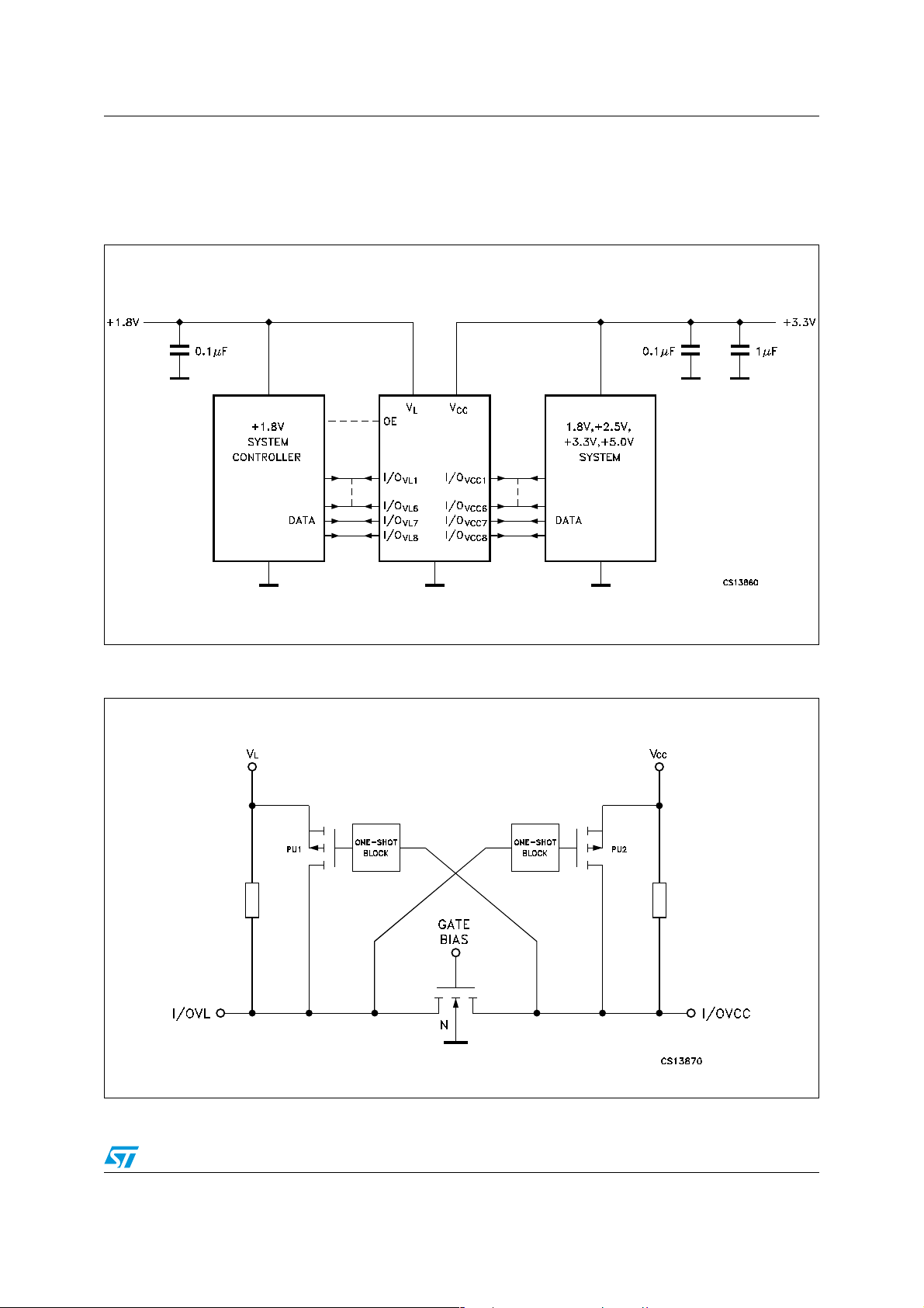
ST2378E Block diagram
1 Block diagram
Figure 1. Block diagram
Figure 2. Functional diagram (1 I/O line)
3/22
Pin settings ST2378E
2 Pin settings
2.1 Pin connection
Figure 3. Pin connection
(Bottom view) Bump side
2.2 Pin description
Table 1. Pin description
Flip-Chip20 Pin N° TSSOP20 Pin N° Symbol Name and function
E2, D1, D2, C1, C2, B1,
B2, A1
E3, D4, D3, C4, C3, B4,
B3, A4
A2 11 OE Output Enable Inputs
A3 10 GND Ground (0V)
E1 1
E4 20
Flip-Chip20
2, 18, 4, 16, 6, 14, 8, 12
19, 3, 17, 5, 15, 7, 13, 9
I/O
I/O
VCC1
TSSOP20 (Top view)
to I/O
VL1
to I/O
V
L
V
CC
VL8
VCC8
Data Inputs/Outputs
Data Inputs/Outputs
Positive Supply Voltage
Positive Supply Voltage
4/22
ST2378E Electrical data
3 Electrical data
3.1 Maximum ratings
Table 2. Absolute maximum rating
Symbol Parameter Value Unit
V
Supply Voltage
L
V
V
V
I/OVL
V
I/OVCC
I
IOVL
I
IOVCC
I
SCTOUT
I
CCB
T
1. 500mW: ≅ 65°C derated to 300mW by 10mW/°C: 65°C to 85°C
Supply Voltage -0.3 to +7.0 V
CC
DC Control Input Voltage -0.3 to +7.0 V
OE
DC I/OVL Input Voltage (OE = Gnd or VL)-0.3 to V
DC I/O
I
DC Input Diode Current (OE Control Pin) − 20 mA
IK
Input Vol tage (OE = Gnd or VL) -0.3 to VCC + 0.3
VCC
DC Output Current ± 25 mA
DC Output Current ± 25 mA
Short Ci rc u it D u ra ti on I/OVL, I/O
Driven from 40mA
VCC
Source
DC VCC or Ground Current
P
Power Dissipation
d
Storage Temperature -65 to +150 °C
stg
T
Lead Temperature (10 sec) 300 °C
L
(1)
-0.3 to V
L
CC
+ 0.3
V
V
V
Continuous mA
± 100 mA
500 mW
5/22
Electrical data ST2378E
3.2 Recommended operating conditions
Table 3. Recommended operating conditions
Symbol Parameter Value Unit
V
V
V
I/OVL
V
I/OVCC
T
dt/dv
Supply Voltage
L
Supply Voltage 1.71 to 5.5 V
CC
Input Voltage (OE Output Enable Pin, VL Power Supply
V
I
referred)
I/OVL Voltage 0 to V
I/O
Voltage 0 to V
VCC
Operating Temperature -40 to 85 °C
op
Input Rise and Fall Time (OE Control Pin)
(1)
1.71 to V
CC
0 to 5.5 V
L
CC
0 to 10 ns/V
V
V
V
1. V
2. V
dt/dv
Input Rise an d Fall T ime
from 10% VL to 90%V
OE
from 10%VL to 90%VL; V
IOVL
1.71 < VL < VCC < 5V
(2)
V
= VL = 5V
CC
L
from 10%VCC to 90%V
IOVCC
CC
0 to 10 ns/V
0 to 3 ns/V
6/22
ST2378E Electrical characteristics
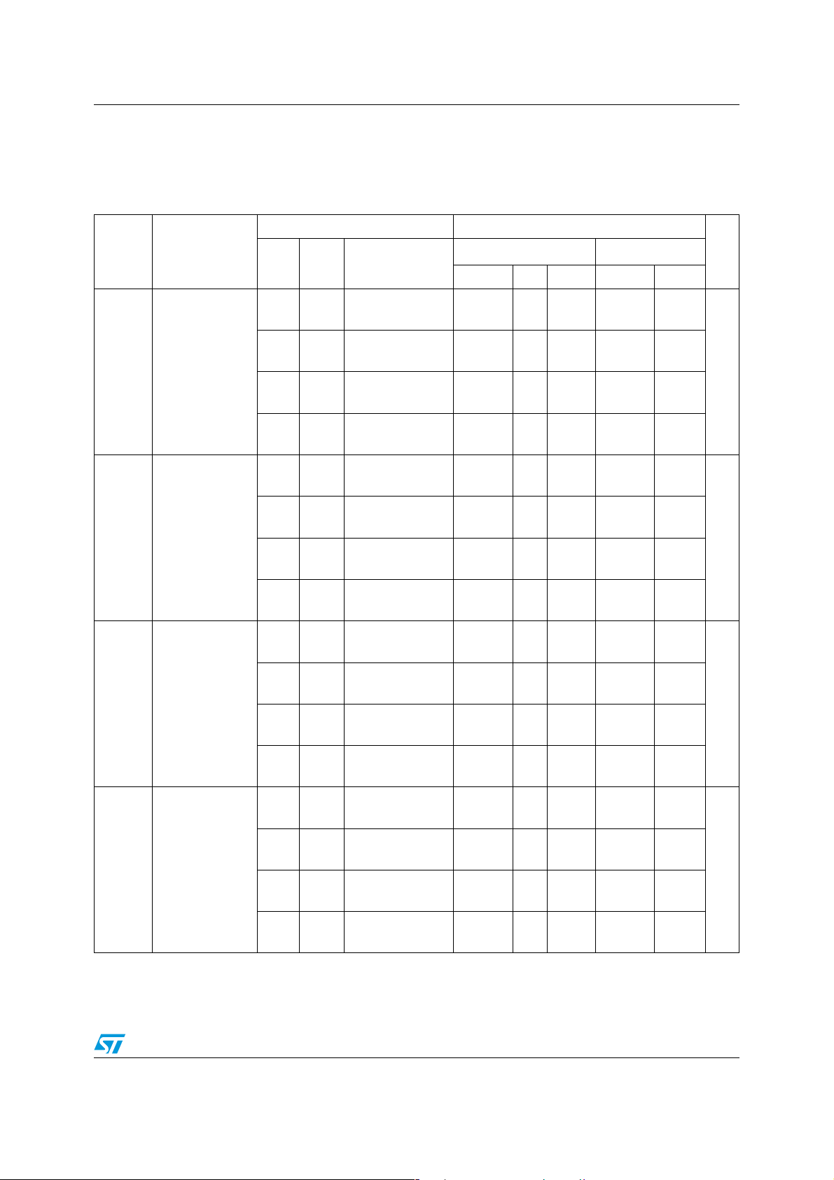
4 Electrical characteristics
Table 4. DC Specification
Test Condition Value
T
Symbol Parameter
V
High Level Input
IHL
Voltage (I/O
VL
V
V
L(*)
CC(*)
(V)
1.8
2.5
)
3.3
5.0
1.8
V
V
V
V
V
(V)
L
5.5
L
5.5
L
5.5
L
5.5
L
5.5
to
to
to
to
to
0.75V
0.75V
0.75V
= 25 °C
A
-40 to 85 °C
Min. Typ Max. Min. Max.
V
-0.2 VL-0.2
L
L
L
L
0.75V
0.75V
0.75V
L
L
L
0.15 0.15
Unit
V
V
to
V
V
V
V
V
V
V
V
V
L
5.5
L
5.5
L
5.5
L
5.5
L
5.5
L
5.5
L
5.5
L
5.5
L
5.5
L
5.5
to
to
to
to
to
to
to
to
to
0.30 0.30
0.30 0.30
0.30 0.30
V
-0.2 VL-0.2
L
0.75V
CC
0.75V
CC
0.75V
CC
0.15 0.15
0.30 0.30
0.30 0.30
0.75V
0.75V
0.75V
V
CC
V
CC
CC
V
V
Low Level Input
ILL
Voltage (I/O
VL
)
3.3
5.0
1.8
2.5
2.5
V
High Level Input
IHC
Voltage (I/O
VCC
)
3.3
5.0
1.8
2.5
V
Low Level Input
ILC
Voltage (I/O
VCC
)
3.3
5.0
V
L
5.5
to
0.30 0.30
7/22

Electrical characteristics ST2378E
Table 4. DC Specification
Test Condition Value
T
Symbol Parameter
V
V
IH-TS
High Level Input
Voltage (OE)
Low Level Input
IL-TS
Voltage (OE)
V
L(*)
(V)
1.8
2.5
3.3
5.0
1.8
2.5
3.3
V
V
V
V
V
V
V
V
CC(*)
(V)
to
L
5.5
to
L
5.5
to
L
5.5
to
L
5.5
to
L
5.5
to
L
5.5
to
L
5.5
0.75V
0.75V
0.75V
= 25 °C
A
-40 to 85 °C
Min. Typ Max. Min. Max.
V
-0.2 VL-0.2
L
L
L
L
0.75V
0.75V
0.75V
L
L
L
0.15 0.15
0.25V
0.25V
L
L
0.25V
0.25V
Unit
V
L
V
L
V
OHL
V
OLL
V
OHC
V
OLC
I
TSL
I
TS-LKG
I
QVCC
High Level
Output Voltage
I/O
VL
Low Level
Output Voltage
I/O
VL
High Level
Output Voltage
I/O
VCC
Low Level
Output Voltage
I/O
VCC
Control Input
Leakage Current
(OE)
High Impedance
Input Leakage
Current (IO
I/O
VCC
,
VL
)
Quiescent
Supply Current
V
CC
5.0
1.8 to
5.5
1.8 to
5.5
1.8 to
5.5
1.8 to
5.5
1.8 to
5.5
V
V
V
V
V
V
L
5.5
L
5.5
L
5.5
L
5.5
L
5.5
L
5.5
to
to
to
to
to
to
I
=-20 µA
O
I/O
VCC≥VCC
IO=1.0 mA
I/O
≤0.15V
VCC
=-20 µA
I
O
I/O
VL≥VL
-0.2
IO=1.0 mA
I/O
≤0.15V
VL
=GNDor5.5
V
I
OE = GND
I/O
I/O
VL,
VCC
unconnected
-0.2
0.67V
0.67V
0.25V
L
L
0.67V
0.25V
L
0.40 0.40
CC
0.67V
CC
0.40 0.40
11µA
11µA
0.1 1 10 µA
L
V
V
8/22

ST2378E Electrical characteristics
Table 4. DC Specification
Test Condition Value
T
Symbol Parameter
V
L(*)
(V)
V
CC(*)
(V)
= 25 °C
A
-40 to 85 °C
Min. Typ Max. Min. Max.
Unit
I
QVL
I
TS-VCC
I
TS-VL
Quiescent
Supply Current
V
L
High Impedance
Mode Quiescent
Supply Current
V
CC
High Impedance
Mode Quiescent
Supply Current
V
L
1.8 to
5.5
1.8 to
5.5
1.8 to
5.5
V
V
V
L
5.5
L
5.5
L
5.5
to
to
to
I/O
I/O
VL,
VCC
unconnected
OE= GND
OE= GND
I/O
=GND to VL
VL
I/O
= GND to
VCC
V
CC
Note: 1 Typical values are referred to TA = 25°C
2 Power Supply Range: V
3 For normal operation, ensure V
, VCC 1.8V ± 5%, 2.5 ± 0.2V, 3.3 ± 0.3V, 5.0 ± 0.5V
L
< (VCC + 0.3V). During power-up, VL > (VCC + 0.3V) will not
L
damage the device
13 20 100 µA
11µA
11µA
9/22

Electrical characteristics ST2378E
Table 5. AC Electrical characteristics (totem pole driving)
T est Condition
C
=15pF tr=tf ≤ 6ns
L
Symbol Parameter
Driver output
R
≤ 50Ω
T
(3)
(V)
V
L
V
CC
1.8 1.8 11 15
1.8 2.5 11 15
t
RVCC
Rise Time I/O
VCC
(3)(8)
1.8 3.3 10 15
1.8 5.0 9 15
2.5 3.3 8 15
1.8 1.8 6 15
1.8 2.5 7 15
t
FCC
Fall Time I/O
VCC
(3)(8)
1.8 3.3 8 15
1.8 5.0 10 15
2.5 3.3 6 15
1.8 1.8 12 15
1.8 2.5 10 15
t
RVL
Rise Time I/O
VL
(3)(8)
1.8 3.3 9 15
1.8 5.0 10 15
2.5 3.3 7 15
1.8 1.8 7 15
1.8 2.5 6 15
t
FVL
Fall Time I/O
VL
(3)(8)
1.8 3.3 6 15
1.8 5.0 7 15
2.5 3.3 4 15
1.8 1.8 6 15
1.8 2.5 7 15
t
PLH
1.8 3.3 7 15
1.8 5.0 7 15
t
IOVL-VCC
Propagation Delay Time(4)
I/O
I/O
VL-LH
VL-HL
to I/O
to I/O
VCC-LH
VCC-HL
2.5 3.3 4 15
1.8 1.8 5 15
1.8 2.5 5 15
t
PHL
1.8 3.3 6 15
1.8 5.0 8 15
2.5 3.3 4 15
(2)
(1)
(V)
(3)
Min.
Value
-40 to +85 °C
(4)
Typ.
Unit
Max.
ns
ns
ns
ns
ns
10/22

ST2378E Electrical characteristics
Table 5. AC Electrical characteristics (totem pole driving)
CC
(V)
Min.
Symbol Parameter
Test Condition
C
=15pF tr=tf ≤ 6ns
L
Driver output
R
≤ 50Ω
T
V
(V) V
L
1.8 1.8 2 15
1.8 2.5 2 15
t
PLH
1.8 3.3 2 15
1.8 5.0 2 15
t
IOVCC-VL
Propagation Delay Time(4)
I/O
I/O
VCC-LH
VCC-HL
to I/O
to I/O
VL-LH
VL-HL
2.5 3.3 2 15
1.8 1.8 5 15
1.8 2.5 5 15
t
PHL
1.8 3.3 5 15
1.8 5.0 6 15
2.5 3.3 4 15
t
PZL tPZH
t
PLZ tPZL
1. For normal operation, ensure VL < (VCC + 0.3V). During power-up, VL > (VCC + 0.3V) will not damage the device
2. For V
3. Power Supply Range: V
4. Typica l values are referr ed to T
5. Rise Time:10% to 90%, Fall Time 90% to 10%
6. tpd: 50% to 50 %
7. Skew is defin ed as the absolute value of the difference between the actual propagation delay for any two outputs of the
8. Each translator equally l oaded; par ameter guaranteed by desi gn
t
OSLH
t
OSHL
Output Enable and Disable Time
Channel to channel Skew T ime
(6)(7)
1.8 1.8 60 80
1.8 5.0 150 200
1.8 1.8 0.1 1
1.8 5.0 0.5 1
DR Maximum Data Rate 1.8 to 5.0
= VL = 1.8V, tr = tf ≤ 4ns
CC
, VCC 1.8V ± 5%, 2.5 ± 0.2V, 3.3 ± 0.3V, 5.0 ± 0.5V.
L
=25°C Ty p ic al values are ref er red to TA=25°C
A
same devi ce switching in the s ame direction, either HIGH o r LOW (t
V
L
OSLH
to 5.0
= | t
13 Mbps
- t
PLHm
PLHn
Value
-40 to +85 °C
Typ.
|, t
= | t
OSHL
PHLm
Max.
- t
PHLn
Unit
ns
ns
ns
|
11/22

Electrical characteristics ST2378E
Table 6. AC characteristic (open drain driving)
Symbol Parameter
t
RVCC
Rise Time I/O
VCC
(3)(8)
T est Condition
=15pF tr=tf ≤ 6ns
C
L
(1)
Driver output
≤ 50Ω
V
CC
(2)
(V)
(3)
Min.
R
T
(3)
(V)
V
L
1.8 1.8 210 300
1.8 5.0 59 150
Value
-40 to +85 °C
(4)
Typ.
Unit
Max.
ns
t
FCC
t
RVL
t
FVL
t
IOVL-VCC
t
IOVCC-VL
t
PZL tPZH
t
PLZ tPZL
t
OSLH
t
OSHL
Fall Time I/O
Rise Time I/O
Fall Time I/O
VCC
VL
VL
(3)(8)
Propagation Delay Time(4)
I/O
I/O
VL-LH
VL-HL
to I/O
to I/O
VCC-LH
VCC-HL
Propagation Delay Time(4)
I/O
I/O
Output Enable and Disable Time
VCC-LH
VCC-HL
to I/O
to I/O
VL-LH
VL-HL
Channel to channel Skew Time
(6)(7)
(3)(8)
(3)(8)
t
t
t
t
PLH
PHL
PLH
PHL
1.8 1.8 12 30
ns
1.8 5.0 20 30
1.8 1.8 210 300
ns
1.8 5.0 96 150
1.8 1.8 11 30
ns
1.8 5.0 11 30
1.8 1.8 210 300
1.8 5.0 100 150
ns
1.8 1.8 7 20
1.8 5.0 14 20
1.8 1.8 210 300
1.8 5.0 57 150
ns
1.8 1.8 7 20
1.8 5.0 8 20
1.8 1.8 60 80
ns
1.8 5.0 150 200
1.8 1.8 10 20
ns
1.8 5.0 2 10
V
DR Maximum Data Rate 1.8 to 5.0
1. For normal operation, ensure VL < (VCC + 0.3V). During power-up, VL > (VCC + 0.3V) will not damage the device
2. For V
3. Power Supply Range: V
4. Typica l values are referr ed to T
5. Rise Time:10% to 90%, Fall Time 90% to 10%
6. tpd: 50% to 50 %
7. Skew is defin ed as the absolute value of the difference between the actual propagation delay for any two outputs of the
8. Each translator equally l oaded; par ameter guaranteed by desi g
= VL = 1.8V, tr = tf ≤ 4ns
CC
, VCC 1.8V ± 5%, 2.5 ± 0.2V, 3.3 ± 0.3V, 5.0 ± 0.5V.
L
=25°C
A
same devi ce switching in the s ame direction, either HIGH o r LOW (t
L
OSLH
to 5.0
= | t
800 kbps
- t
|, t
PLHm
PLHn
OSHL
= | t
PHLm
- t
PHLn
|
12/22

ST2378E Test circuit
5 Test circuit
Figure 4. Test circuit
Note: C
Table 7. Test circuit switches
Test
t
, t
PLH
PHL
t
, t
PZL
PLZ
t
, t
PZH
PHZ
= 15/50pF or equivalent (includes jig and probe capacitance)
L
= 1KΩ or equivalent
R
1
R
T
= Z
of pulse generator (typically 50Ω)
OUT
Drivi n g I/ O
VL
Open Open Open
V
CC
Gnd Gnd -
Switch
Driving I/O
V
L
Table 8. Truth table
Control Pin Bidirectional Input/Outputs
OE
(1)
H
(1)
H
LZ Z
1. High Level VL Power Supply referred
2. High Level VCC Power Supply referred
I/O
VL
(1)
H
LL
VCC
Open Drain Driving
-
I/O
VCC
(2)
H
Note: X= Do not care; Z = High Impedance;
13/22

Waveforms ST2378E
6 Waveforms
Table 9. Waveform symbol value
Drivi ng I/ O
≤ 2.5V 3.3V ≤ VL≤ V
CC
V
CC
CC
CC
VCC
V
CC
50% V
50% V
CC
CC
CC
≤ 5.0V
Symbol
V
IH
V
IM
V
OM
V
X
V
Y
Drivi n g I/O
1.8V ≤ VL≤ V
50% V
50% V
≤ 2.5V 3.3V ≤ VL≤ V
CC
V
L
L
CC
VOL +0.15V VOL +0.3V VOL +0.15V VOL +0.3V
VOH -0.15V VOH -0.3V VOH -0.15V VOH -0.3V
VL
V
50% V
50% V
≤ 5.0V 1.8V ≤ VL≤ V
CC
L
L
CC
50% V
50% V
Figure 5. Waveform - propagation delay (f = 1MHz; 50% duty cycle)
14/22

ST2378E Waveforms
Figure 6. Waveform - output enable and disable time (f = 1MHz; 50% duty cycle)
15/22

Package mechanical data ST2378E
7 Package mechanical data
In order to meet environmental requirements, ST offers these devices in ECOPA CK ®
packages. These packages have a Lead-free second level interconnect . The category of
second level interconnect is marked on the package and on the inner box label, in
compliance with JEDEC Standard JESD97. The maximum ratings related to soldering
conditions are also marked on the inner box label. ECOPACK is an ST trademark.
ECOPACK specifications are available at: www.st.com
16/22

ST2378E Package mechanical data
Figure 7. TSSOP20 Mechanical data
TSSOP20 MECHANICAL DATA
DIM.
A 1.2 0.047
A1 0.05 0.15 0.002 0.004 0.006
A2 0.8 1 1.05 0.031 0.039 0.041
b 0.19 0.30 0.007 0.012
c 0.09 0.20 0.004 0.0079
D 6.4 6.5 6.6 0.252 0.256 0.260
E 6.2 6.4 6.6 0.244 0.252 0.260
E1 4.3 4.4 4.48 0.169 0.173 0.176
e 0.65 BSC 0.0256 BSC
K0˚ 8˚0˚ 8˚
L 0.45 0.60 0.75 0.018 0.024 0.030
MIN. TYP MAX. MIN. TYP. MAX.
A2
A
A1
mm. inch
b
e
c
K
L
E
PIN 1 IDENTIFICATION
D
E1
1
0087225C
17/22

Package mechanical data ST2378E
Figure 8. Flip-Chip20 Mechanical data
Flip-Chip20 MECHANICAL DATA
DIM.
MIN. TYP MAX. MIN. TYP. MAX.
A 0.810.891.0031.935.039.4
A1 0.15 0.24 0.35 5.9 9.4 13.8
A2 0.65 25.6
b 0.25 0.30 0.35 9.8 11.8 13.8
D 2.412.462.5194.996.998.8
D1 2.00 78.7
E 1.931.982.0376.078.079.9
E1 1.5 59.1
e0.50 19.7
SE 0.25 9.8
mm. mils
18/22
7487339-D

ST2378E Package mechanical data
Figure 9. TSSOP20 Tape and reel
Tape & Reel TSSOP20 MECHANICAL DATA
DIM.
MIN. TYP MAX. MIN. TYP. MAX.
A 330 12.992
C 12.8 13.2 0.504 0.519
D 20.2 0.795
N 60 2.362
T 22.4 0.882
Ao 6.8 7 0.268 0.276
Bo 6.9 7.1 0.272 0.280
Ko 1.7 1.9 0.067 0.075
Po 3.9 4.1 0.153 0.161
P 11.9 12.1 0.468 0.476
mm. inch
19/22

Package mechanical data ST2378E
Figure 10. Flip-Chip20 Tape and reel
Tape & Reel Flip-Chip20 MECHANICAL DATA
DIM.
MIN. TYP MAX. MIN. TYP. MAX.
A 180 7.086
C 12.8 13.2 0.504 0.519
D 20.2 0.795
N 60 2.362
T 14.4 0.567
Ao 2.13 2.23 2.33 0.084 0.088 0.092
Bo 2.62 2.72 2.82 0.103 0.107 0.111
Ko 1.05 1.15 1.25 0.041 0.045 0.049
Po 3.9 4.1 0.153 0.161
P 3.9 4.1 0.153 0.161
mm. inch
20/22

ST2378E Revision history
8 Revision history
Table 10. Revision history
Date Revision Changes
10-Apr-2006 1 Initial release.
21/22

ST2378E
I
e
r
y
t
A
P
o
l
N
is
d
ts
o
h
t
U
D
W
D
W
S
O
U
D,
A
S,
N
R
S
R
id
a
y
l
Please Read Caref u ll y:
nformation in this document is provided solely in connection with ST products. STMicroelectronics NV and its subsidiaries (“ST”) reserve th
ight to make changes, corrections, modifications or improvements, to this document, and the products and services described herein at an
ime, without notice.
ll ST product s are sold pursuant to ST’ s te rm s and condit io ns of sale.
urchasers are solely responsible for the choice, selection and use of the ST products and servi ces descri bed herein, and ST assumes n
iability whatsoever relating to the choice, selection or use of the ST products and services described herein.
o license, express or implied, by estoppel or otherwise, to any intellectual property rights is granted under this document. If any part of th
ocument refers to any third par ty products or services i t s hall not be d eem ed a licen se grant by ST f or the use of such third party produc
r services , or any intel lec tual pro per ty cont aine d ther ein or con sidere d as a warra nty c overi ng th e use i n any mann er w hats oever of suc
hird part y products or services or any i n t el l ectual property contained therein.
NLESS OTHERWISE SET FORTH IN ST’S TERMS AND CONDITIONS OF SALE ST DISCLAIMS ANY EXPRESS OR IMPLIE
ARRANTY WITH RESPECT TO THE USE AND/OR SALE OF ST PRODUCTS INCLUDING WITHOUT LIMITATION IMPLIE
ARRANTIES OF MERCHANTABILITY, FITNESS FOR A PARTICULAR PURPOSE (AND THEIR EQUIVALENTS UNDER THE LAW
F ANY JURISDICTION), OR INFRINGEMENT OF ANY PATENT, COPYRIGHT OR OTHER INTELLECTUAL PROPERTY RIGHT.
NLESS EXPRESSLY APPROVED IN WRI TING BY A N AUTH ORIZE REP RESENTATI VE OF S T, ST PRODUCTS ARE NOT DESIGNE
UTHORIZ ED OR WARRANTED F OR USE IN MILITARY , AIR CRAF T , S PACE, L IF E SAVING , O R LIFE SUSTAINING AP PL ICATION
OR IN PRODUCTS OR SYSTEMS, WHERE FAILURE OR MALFUNCTION MAY RESULT IN PERSONAL INJURY, DEATH, O
EVERE PROPERTY OR ENVIRONMENTAL DAMAGE.
esale of ST products with provisions different from the statements and/or technical features set forth in this document shall immediately vo
ny warran ty gr anted by ST fo r the ST produc t or se rvice d es cribed he rein and shall not c reat e o r extend in a ny mann er wha tsoe ve r, an
iability of ST.
The ST logo is a registered trademark of STMicroelectronics. All other names are the property of their respective owners.
ST and the ST logo are trademarks or regis t ered trademarks of ST in vari ous countri es.
Information in this docum ent supersedes and replaces all information previously supplied.
© 2006 STMi croelectro ni cs - All rights reserved
Austra l i a - Be l gi um - Brazil - Canada - China - Czech Rep ubl i c - Finland - F rance - Germany - Hong Kon g - India - Israel - Italy - Japan -
STMicroelectron ics group of com panies
Malaysi a - M al ta - Morocco - Singapore - Spain - Sweden - Switze rl and - Unite d Kingdom - Unit ed States of America
www.st.com
22/22
 Loading...