

Features
■ 90 Mbps (max) data rate when driven by a
totem pole driver
■ 8 Mbps (max) data rate when driven by an
open drain pole driver
■ Bi-directional level translation without
direction control pin
■ Wide V
■ Wide V
■ Power down mode feature – when either
supply is off, all I/Os are in high impedance
■ Low quiescent current (max 24 µA)
■ Able to be driven by totem pole and open drain
drivers
■ 5.5 V tolerant enable pin
■ ESD performance on all pins: ±2 kV HBM
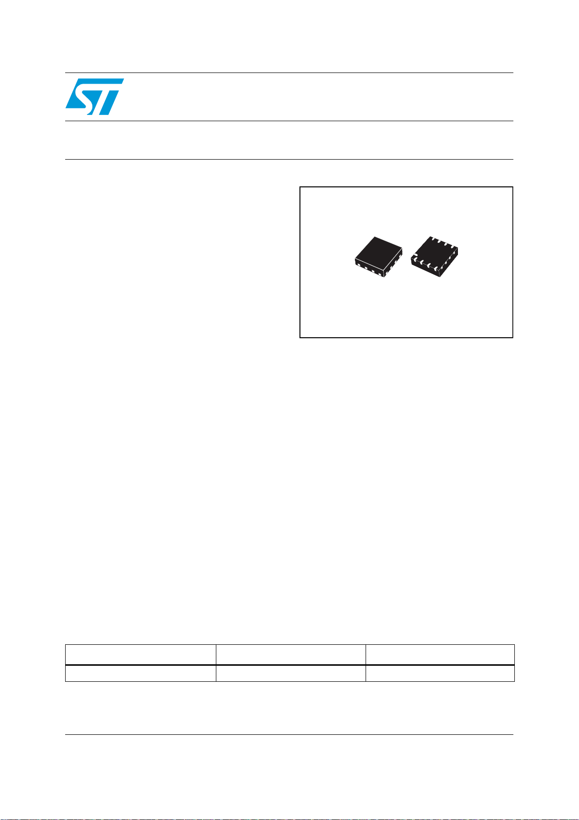
■ Small package and footprint
QFN16 (2.6 x 1.8 mm) package
voltage range of 1.65 to 3.6 V
L
voltage range of 1.80 to 5.5 V
CC
ST2349
4-bit dual supply level translator
without direction control pin
QFN16L
(2.6 x 1.8 mm)
Description
The ST2349 is a 4-bit dual supply level translator
which provides the level shifting capability to allow
data transfer in a multi-voltage system. Externally
applied voltages, V
on either side of the device. It utilizes
transmission gate-based design that allows bidirectional level translation without a control pin.
and VL, set the logic levels
CC
Applications
■ Low voltage system level translation
■ Mobile phones and other mobile devices
2
■ I
C level translation
■ UART level translation
The ST2349 accepts a V
V
from 1.80 to 5.5 V, making it ideal for data
CC
transfer between low-voltage ASICs/PLD and
higher voltage systems. This device has a tri-state
output mode which can be used to disable all
I/Os.
The ST2349 supports power down mode when
V
is grounded/floating and the device is
CC
from 1.65 to 3.6 V and
L
disabled via the OE pin.
Table 1. Device summary
Order code Package Packaging
ST2349QTR QFN16 (2.6 x 1.8 mm) Tape and reel (3000 parts per reel)
May 2008 Rev 4 1/23
www.st.com
23

Contents ST2349
Contents
1 Pin settings . . . . . . . . . . . . . . . . . . . . . . . . . . . . . . . . . . . . . . . . . . . . . . . . 5
1.1 Pin connection . . . . . . . . . . . . . . . . . . . . . . . . . . . . . . . . . . . . . . . . . . . . . . 5
1.2 Pin description . . . . . . . . . . . . . . . . . . . . . . . . . . . . . . . . . . . . . . . . . . . . . . 5
2 Device block diagrams . . . . . . . . . . . . . . . . . . . . . . . . . . . . . . . . . . . . . . . 6
3 Supplementary notes . . . . . . . . . . . . . . . . . . . . . . . . . . . . . . . . . . . . . . . . 7
3.1 Driver requirement . . . . . . . . . . . . . . . . . . . . . . . . . . . . . . . . . . . . . . . . . . . 7
3.2 Load driving capability . . . . . . . . . . . . . . . . . . . . . . . . . . . . . . . . . . . . . . . . 7
3.3 Power off feature . . . . . . . . . . . . . . . . . . . . . . . . . . . . . . . . . . . . . . . . . . . . 7
3.4 Truth table . . . . . . . . . . . . . . . . . . . . . . . . . . . . . . . . . . . . . . . . . . . . . . . . . . 7
4 Maximum rating . . . . . . . . . . . . . . . . . . . . . . . . . . . . . . . . . . . . . . . . . . . . . 8
4.1 Recommended operating conditions . . . . . . . . . . . . . . . . . . . . . . . . . . . . . 8
5 Electrical characteristics . . . . . . . . . . . . . . . . . . . . . . . . . . . . . . . . . . . . . 9
5.1 AC characteristics (device driven by open drain driver) . . . . . . . . . . . . . . 11
5.2 AC characteristics (device driven by totem pole driver ) . . . . . . . . . . . . . 13
6 Waveforms . . . . . . . . . . . . . . . . . . . . . . . . . . . . . . . . . . . . . . . . . . . . . . . . 16
7 Package mechanical data . . . . . . . . . . . . . . . . . . . . . . . . . . . . . . . . . . . . 18
8 Revision history . . . . . . . . . . . . . . . . . . . . . . . . . . . . . . . . . . . . . . . . . . . 22
2/23

ST2349 List of figures
List of figures
Figure 1. ST2349 pin connection (top through view) . . . . . . . . . . . . . . . . . . . . . . . . . . . . . . . . . . . . . 5
Figure 2. ST2349 block diagram . . . . . . . . . . . . . . . . . . . . . . . . . . . . . . . . . . . . . . . . . . . . . . . . . . . . . 6
Figure 3. Application block diagram . . . . . . . . . . . . . . . . . . . . . . . . . . . . . . . . . . . . . . . . . . . . . . . . . . . 6
Figure 4. Test circuit . . . . . . . . . . . . . . . . . . . . . . . . . . . . . . . . . . . . . . . . . . . . . . . . . . . . . . . . . . . . . 15
Figure 5. Waveform - propagation delay (f = 1 MHz; 50% duty cycle). . . . . . . . . . . . . . . . . . . . . . . . 16
Figure 6. Waveform - output enable and disable time (f = 1 MHz; 50% duty cycle) . . . . . . . . . . . . . 17
Figure 7. QFN16L (2.6 x 1.8 mm) package outline . . . . . . . . . . . . . . . . . . . . . . . . . . . . . . . . . . . . . . 18
Figure 8. QFN16L (2.6 x 1.8 mm) footprint recommendation . . . . . . . . . . . . . . . . . . . . . . . . . . . . . . 19
Figure 9. QFN16L (2.6 x 1.8 mm) carrier tape. . . . . . . . . . . . . . . . . . . . . . . . . . . . . . . . . . . . . . . . . . 20
Figure 10. QFN16L (2.6 x 1.8 mm) reel information . . . . . . . . . . . . . . . . . . . . . . . . . . . . . . . . . . . . . . 21
3/23

List of tables ST2349
List of tables
Table 1. Device summary . . . . . . . . . . . . . . . . . . . . . . . . . . . . . . . . . . . . . . . . . . . . . . . . . . . . . . . . . . 1
Table 2. ST2349 pin description . . . . . . . . . . . . . . . . . . . . . . . . . . . . . . . . . . . . . . . . . . . . . . . . . . . . . 5
Table 3. Truth table. . . . . . . . . . . . . . . . . . . . . . . . . . . . . . . . . . . . . . . . . . . . . . . . . . . . . . . . . . . . . . . 7
Table 4. Absolute maximum ratings . . . . . . . . . . . . . . . . . . . . . . . . . . . . . . . . . . . . . . . . . . . . . . . . . . 8
Table 5. Recommended operating conditions . . . . . . . . . . . . . . . . . . . . . . . . . . . . . . . . . . . . . . . . . . 8
Table 6. DC characteristics (over recommended operating conditions unless otherwise noted. All typ-
ical values are at T
Table 7. AC characteristics - test conditions: V
tr = tf ≤ 2 ns) over temperature range -40 °C to 85 °C11
Table 8. AC characteristics - test conditions: V
tr = tf ≤ 2 ns) over temperature range -40 °C to 85 °C11
Table 9. AC characteristics - test conditions: V
tr = tf ≤ 2 ns) over temperature range -40 °C to 85 °C12
Table 10. AC characteristics (test conditions: V
tr = tf ≤ 2 ns) over temperature range -40 °C to 85 °C)13
Table 11. AC characteristics (test conditions: V
tr = tf ≤ 2 ns) over temperature range -40 °C to 85 °C)13
Table 12. AC characteristics (test conditions: V
tr = tf ≤ 2 ns) over temperature range -40 °C to 85 °C)14
Table 13. Test circuit switches . . . . . . . . . . . . . . . . . . . . . . . . . . . . . . . . . . . . . . . . . . . . . . . . . . . . . . 15
Table 14. Waveform symbol value . . . . . . . . . . . . . . . . . . . . . . . . . . . . . . . . . . . . . . . . . . . . . . . . . . . 16
Table 15. QFN16L (2.6 x 1.8 mm) mechanical data . . . . . . . . . . . . . . . . . . . . . . . . . . . . . . . . . . . . . . 19
Table 16. Document revision history . . . . . . . . . . . . . . . . . . . . . . . . . . . . . . . . . . . . . . . . . . . . . . . . . 22
= 25 oC)
A
= 1.65 - 1.8 V (load CL=15pF; Rup=4.7kΩ; driver
L
= 2.5 - 2.7 V (load CL=15pF; Rup=4.7kΩ; driver
L
= 2.7 - 3.6 V (load CL=15pF; Rup=4.7kΩ; driver
L
= 1.65 - 1.8 V (load CL=15pF; Rup=10kΩ; driver
L
= 2.5 - 2.7 V (load CL=15pF; Rup=10kΩ; driver
L
= 2.7 - 3.6 V (load CL=15pF; Rup=10kΩ; driver
L
4/23
ST2349 Pin settings
1 Pin settings
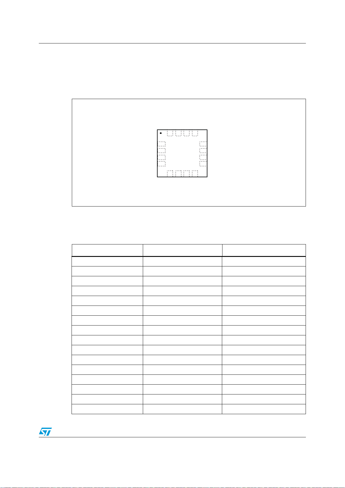
1.1 Pin connection
Figure 1. ST2349 pin connection (top through view)
1.2 Pin description
Table 2. ST2349 pin description
Pin number Symbol Name and function
1I/O
2 OE Output enable
3I/O
4I/O
5 NC No connection
6V
7V
8 NC No connection
9 I/O
10 I/O
11 GND Ground
I/O
I/O
I/O
VL2
OE
VL3
VL4
L
VL2
VL3
VL4
CC
VCC1
13 14 15 16
I/O
12
VCC2
11
GND
I/O
10
VCC3
9
O/I
VCC4
8
7
NC
CC
V
CS00022
Data input/output
Data input/output
Data input/output
L
Supply voltage
Supply voltage
Data input/output
Data input/output
VL1
I/O
VL VCC I/O
1
2
3
4
5
6
V
NC
VCC4
VCC3
12 I/O
13 I/O
14 V
15 V
16 I/O
5/23
VCC2
VCC1
CC
L
VL1
Data input/output
Data input/output
Supply voltage
Supply voltage
Data input/output
Device block diagrams ST2349
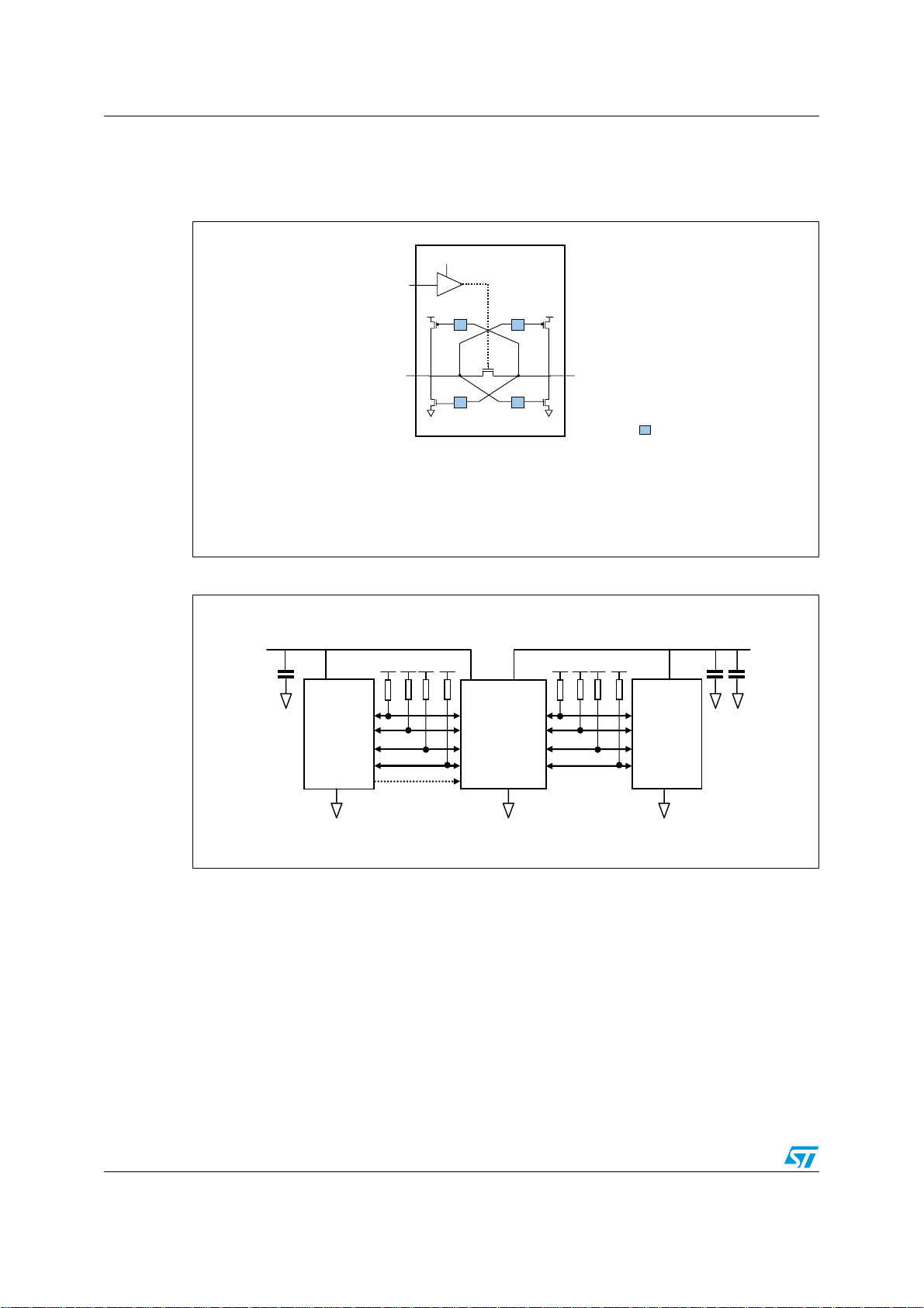
2 Device block diagrams
Figure 2. ST2349 block diagram
ST2349
VL
OE
I/O
VL
EN
VL
VCC
I/O
VCC
GND
* ST2349 has 4 channels. For simplicity, the above diagram shows only 1 channel.
* When OE is low, all I/Os are in high-impedance mode.
Figure 3. Application block diagram
V
L
0.1
μ
F
VL
system
controller
V
V
V
L VL
L
L
OE
I/O
I/O
I/O
I/O
GND
VCCVCCVCCV
V
V
L
CC
I/O
VL1
VCC1
I/O
VL2
VCC2
I/O
VL3
VCC3
I/O
VCC4
VL4
CC
= one-shot circuit
CC
V
system
controller
0.1 μF
1μF
CS00021
V
CD00023
CC
6/23
ST2349 Supplementary notes
3 Supplementary notes
3.1 Driver requirement
The ST2349 may be driven by an open drain or totem pole driver and the nature of the
device’s output is “open drain”. It must not be used to drive a pull-down resistor since the
impedance of the output at HIGH state depends on the pull-up resistor placed at the I/Os.
As the device has pull-up resistors on both the I/O
ensure that the driver is able to sink the required amount of current. For example, if the
settings are V
=5.5V, VL= 4.3 V and the pull-up resistor is 10 kΩ, then the driver must be
CC
able to sink at least (5.5 V/10 kΩ) + (4.3 V/10 kΩ)
requirements of the ST2349.
3.2 Load driving capability
To support the open drain system, the one-shot transistor is turned on only during state
transition at the output side. When it drives a high state, after the one-shot transistor is
turned off, only the pull-up resistor is able to maintain the state. In this case, the resistive
load is not recommended.
During the translation from V
side to VL side, the oscillation might be triggered when the
CC
signal is reflected back as a glitch. This is caused by the architecture of the device (auto-
direction).
When using the ST2349, care need to be taken in the PCB data-track design and output
loading. It is recommended that the load is less than 25 pf.
3.3 Power off feature
In some applications where it might be required to turn off one of the power supplies
powering up the level translator, the user may turn off the V
(device is disabled). There will be no current consumption in V
other causes, and the I/Os are in a high-impedance state in this mode.
and I/OVL ports, the user needs to
VCC
= 1 mA and still meet the V
only when the OE pin is low
CC
due to floating gates or
L
IL
3.4 Truth table
Table 3. Truth table
Enable Bi-directional Input/Output
OE I/O
(1)
H
(1)
H
L Z
1. High level VL power supply referred
2. High level VCC power supply referred
3. Z = high impedance
VCC
(2)
H
L L
(3)
7/23
I/O
H
Z
(1)
(3)
VL
 Loading...