

ST ST202EB, ST202EC, ST232EB, ST232EC User Manual
± 15 kV ESD protected 5 V RS-232 transceiver
Features
■ ESD protection for RS-232 I/O pins:
■ ± 15 kV human body model
■ Guaranteed 230 kbps date rate
■ Guaranteed slew rate range 3 to 30 V/ms
■ Operate from a single 5 V power supply
Description
The ST202E/ST232E are a 2 driver 2 receiver
devices designed for RS-232 and V.28
communications in harsh environments. Each
transmitter output and receiver input is protected
against ± 15 kV electrostatic discharge (ESD)
shocks. The drivers meet all EIA/TIA-232E and
CCITT V.28 specifications at data rates up to 230
kbps, when loaded in accordance with the
EIA/TIA-232E specification. The ST202E/232E
use a single 5 V supply voltage.
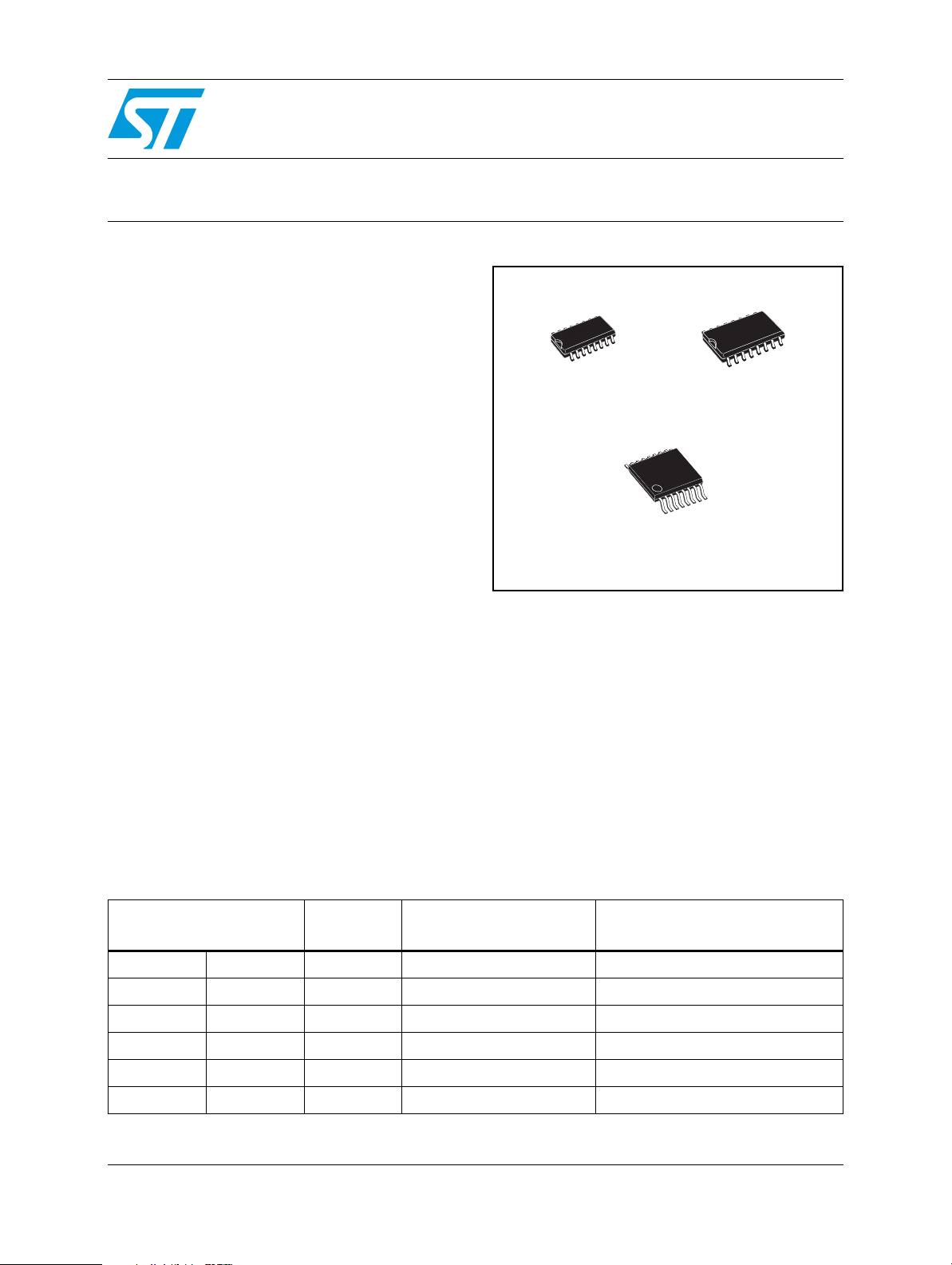
ST202EB - ST202EC
ST232EB - ST232EC
SOP
TSSOP
SOP Large
The ST232E operates with four 1 µF capacitors,
while the ST202E operates with four 0.1 µF
capacitors, further reducing cost and board
space.
Table 1. Device summary
Order codes
ST202ECDR ST232ECDR 0 to 70 °C SO-16 (tape & reel) 2500 parts per reel
ST202EBDR ST232EBDR -40 to 85 °C SO-16 (tape & reel) 2500 parts per reel
ST232ECWR 0 to 70 °C SO-16 large (tape & reel) 1000 parts per reel
ST202EBWR -40 to 85 °C SO-16 large (tape & reel) 1000 parts per reel
ST202ECTR ST232ECTR 0 to 70 °C TSSOP16 (tape & reel) 2500 parts per reel
ST202EBTR ST232EBTR -40 to 85 °C TSSOP16 (tape & reel) 2500 parts per reel
Temperature
range
Packages Packaging
February 2008 Rev 16 1/18
www.st.com
18

ST202EB - ST202EC - ST232EB - ST232EC
Contents
1 Pin configuration . . . . . . . . . . . . . . . . . . . . . . . . . . . . . . . . . . . . . . . . . . . 3
2 Maximum ratings . . . . . . . . . . . . . . . . . . . . . . . . . . . . . . . . . . . . . . . . . . . . 4
3 Electrical characteristics . . . . . . . . . . . . . . . . . . . . . . . . . . . . . . . . . . . . . 5
4 Typical application . . . . . . . . . . . . . . . . . . . . . . . . . . . . . . . . . . . . . . . . . . 7
5 Typical performance characteristics . . . . . . . . . . . . . . . . . . . . . . . . . . . . 8
6 Package mechanical data . . . . . . . . . . . . . . . . . . . . . . . . . . . . . . . . . . . . 10
7 Revision history . . . . . . . . . . . . . . . . . . . . . . . . . . . . . . . . . . . . . . . . . . . 17
2/18
ST202EB - ST202EC - ST232EB - ST232EC Pin configuration
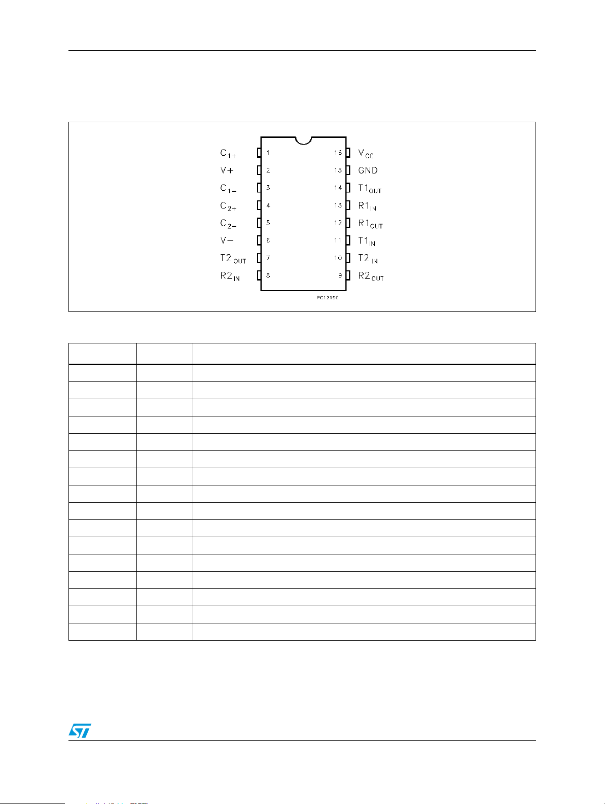
1 Pin configuration
Figure 1. Pin connections (top view)
Table 2. Pin description
Pin n° Symbol Note
1C
2 V+ Doubled voltage terminal
3C
4C
5C
6 V- Inverted voltage terminal
7T2
8R2
9R2
10 T2
11 T1
12 R1
13 R1
14 T1
15 GND Ground
16 V
+ Positive terminal for the first charge pump capacitor
1
- Negative terminal for the first charge pump capacitor
1
+ Positive terminal for the second charge pump capacitor
2
- Negative terminal for the second charge pump capacitor
2
OUT
OUT
OUT
OUT
CC
Second transmitter output voltage
Second receiver input voltage
IN
Second receiver output voltage
Second transmitter input voltage
IN
First transmitter input voltage
IN
First receiver output voltage
First receiver input voltage
IN
First transmitter output voltage
Supply voltage
3/18
Maximum ratings ST202EB - ST202EC - ST232EB - ST232EC
2 Maximum ratings
Table 3. Absolute maximum ratings
Symbol Parameter Value Unit
V
CC
V+ Extra positive voltage (V
Supply voltage -0.3 to 6 V
-0.3) to 14 V
CC
V- Extra negative voltage -14 to 0.3 V
T
R
T
OUT
R
OUT
T
SCTOUT
T
STG
IN
IN
Transmitter input voltage range -0.3 to (V+ + 0.3) V
Receiver input voltage range ± 30 V
Transmitter output voltage range (V- - 0.3) to (V+ + 0.3) V
Receiver output voltage range -0.3 to (VCC + 0.3) V
Short circuit duration on T
OUT
infinite
Storage temperature range -65 to 150 °C
Note: Absolute maximum ratings are those values beyond which damage to the device may occur.
Functional operation under these condition is not implied.
4/18
ST202EB - ST202EC - ST232EB - ST232EC Electrical characteristics
3 Electrical characteristics
Table 4. ESD performance: transmitter outputs, receiver inputs
Symbol Parameter Test condition Min. Typ. Max. Unit
ESD ESD protection voltage Human Body Model ± 15 kV
ESD ESD protection voltage IEC 1000-4-2 (Contact Discharge) ± 6kV
ESD ESD protection voltage IEC 1000-4-2 (Air Discharge) ± 8kV
Note: All test versus GND.
Table 5. Electrical characteristics
(C
- C4 = 0.1 µF for ST202E, C1 - C4 = 0.1 µF for ST232E, VCC = 5 V ± 10 %,
1
= -40 to 125 °C, unless otherwise specified. Typical values are referred to TA = 25 °C).
T
A
Symbol Parameter Test condition Min. Typ. Max. Unit
I
SUPPLY
VCC power supply current No Load, TA = 25°C 5 10 mA
Table 6. Transmitter electrical characteristics
(C
- C4 = 0.1 µF, VCC = 5 V ± 10 %, TA = -40 to 85 °C, unless otherwise specified. Typical
1
values are referred to T
Symbol Parameter Test condition Min. Typ. Max. Unit
V
R
TOUT
I
TIL
V
V
TIH
SR
D
TOUT
I
SC
t
DT
Output voltage swing
Input leakage current ± 10 µA
Input logic threshold low 0.8 V
TIL
Input logic threshold high 2 V
Transition slew rate
T
Data rate
R
Transmitter output resistance VCC = V+ = V- = 0V V
Transmitter output short circuit
current
Transmitter propagation delay
= 25 °C).
A
All Transmitter outputs are loaded
with 3 kΩ to GND
= 25°C, VCC = 5 V RL = 3 to 7
T
A
KΩ, CL = 50 to 1000 pF
R
= 3 to 7 kΩ, CL = 50 to 1000 pF
L
one transmitter switching
= 3 to 7 kΩ, CL = 50 to 2500 pF
R
L
All transmitter loaded
± 5 ± 9V
(1)
3630V/µs
230 400 kbits/s
= ± 2 V 300 Ω
OUT
±10 ±60 mA
2µA
1. Measured from 3 V to -3 V or from -3 V to 3 V
2. One transmitter output is loaded with R
= 3 kΩ to 7 kΩ, CL = 50 to 1000 pF
L
5/18
Electrical characteristics ST202EB - ST202EC - ST232EB - ST232EC
Table 7. Receiver electrical characteristics
(C
- C4 = 0.1 µF, VCC = 5 V ± 10 %, TA = -40 to 85 °C, unless otherwise specified. Typical
1
values are referred to T
Symbol Parameter Test condition Min. Typ. Max. Unit
= 25 °C).
A
V
R
V
V
V
RIHYS
V
V
t
RIN
RIN
RIL
RIH
ROL
ROH
DR
Receiver input voltage
operating range
-30 30 V
RS-232 input resistance TA = 25°C, VCC = 5 V 3 5 7 kΩ
RS-232 input logic threshold
low
RS-232 input logic threshold
high
T
= 25°C, VCC = 5 V 0.8 1.2 V
A
= 25°C, VCC = 5 V 1.7 2.4 V
T
A
RS-232 input hysteresis VCC = 5 V 0.2 0.5 1 V
TTL/CMOS output voltage low I
TTL/CMOS output voltage high I
= 3.2 mA 0.4 V
OUT
= -1 mA 3.5 VCC-0.4 V
OUT
Receiver propagation delay CL = 150 pF 0.5 10 µs
6/18
 Loading...