

ST ST2329B User Manual
ST2329B
2-bit dual supply level translator without direction control pin, open
drain output
Datasheet − preliminary data
Features
■ 18 Mbps (max.) data rate when driven by
a totem pole driver
■ 6.8 Mbps (max.) data rate when driven by an
open drain pole driver
■ Bi-directional level translation without
direction control pin
■ Wide V
■ Wide V
■ Power-down mode feature: when either supply
is OFF, all I/Os are in high impedance
■ Low quiescent current (max. 4 µA)
■ Able to be driven by totem pole and open drain
drivers
■ 5.5 V tolerant Enable pin
■ ESD performance on all pins: ±2 kV HBM
■ Small package and footprint:
QFN8 (1.4 x 1.2 x 0.55 mm) package
Applications
voltage range of 1.65 to 3.6 V
L
voltage range of VL to 5.5 V
CC
QFN8
(1.4 x 1.2 x 0.55 mm)
Table 1. Device summary
Order code Package Packing
Tape and
reel (3000
parts per
reel)
ST2329BQTR
QFN8
(1.4 x 1.2 x
0.55 mm)
Package
topmark
3A
■ Low-voltage system level translation
■ Mobile phones and other mobile devices
2
■ I
C level translation
■ UART level translation
June 2012 Doc ID 023359 Rev 1 1/22
This is preliminary information on a new product now in development or undergoing evaluation. Details are subject to
change without notice.
www.st.com
1

Contents ST2329B
Contents
1 Description . . . . . . . . . . . . . . . . . . . . . . . . . . . . . . . . . . . . . . . . . . . . . . . . . 5
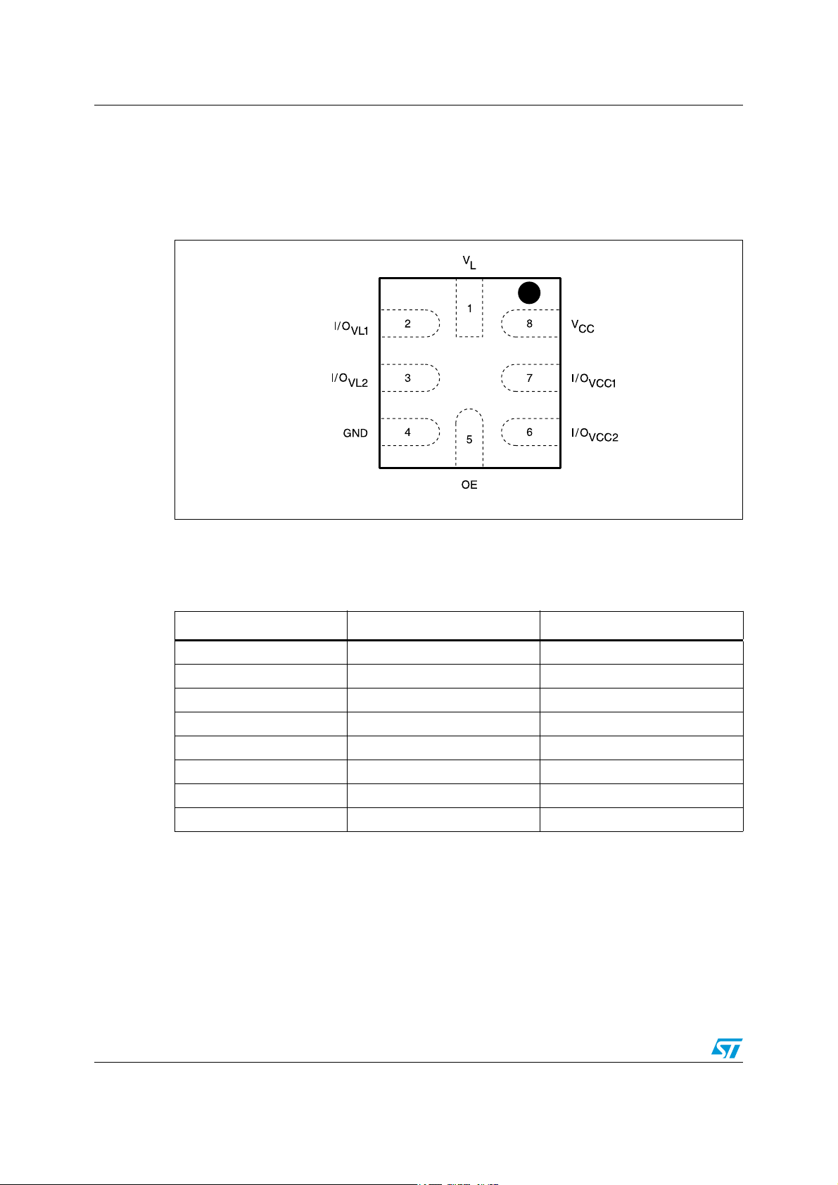
2 Pin settings . . . . . . . . . . . . . . . . . . . . . . . . . . . . . . . . . . . . . . . . . . . . . . . . 6
2.1 Pin connection . . . . . . . . . . . . . . . . . . . . . . . . . . . . . . . . . . . . . . . . . . . . . . 6
2.2 Pin description . . . . . . . . . . . . . . . . . . . . . . . . . . . . . . . . . . . . . . . . . . . . . . 6
3 Device block diagrams . . . . . . . . . . . . . . . . . . . . . . . . . . . . . . . . . . . . . . . 7
4 Supplementary notes . . . . . . . . . . . . . . . . . . . . . . . . . . . . . . . . . . . . . . . . 8
4.1 Driver requirements . . . . . . . . . . . . . . . . . . . . . . . . . . . . . . . . . . . . . . . . . . 8
4.2 Load driving capability . . . . . . . . . . . . . . . . . . . . . . . . . . . . . . . . . . . . . . . . 8
4.3 Power-off feature . . . . . . . . . . . . . . . . . . . . . . . . . . . . . . . . . . . . . . . . . . . . 8
4.4 Truth table . . . . . . . . . . . . . . . . . . . . . . . . . . . . . . . . . . . . . . . . . . . . . . . . . . 8
5 Maximum rating . . . . . . . . . . . . . . . . . . . . . . . . . . . . . . . . . . . . . . . . . . . . . 9
Recommended operating conditions . . . . . . . . . . . . . . . . . . . . . . . . . . . . . . . . . . . 9
6 Electrical characteristics . . . . . . . . . . . . . . . . . . . . . . . . . . . . . . . . . . . . 10
6.1 DC characteristics . . . . . . . . . . . . . . . . . . . . . . . . . . . . . . . . . . . . . . . . . . 10
6.2 AC characteristics . . . . . . . . . . . . . . . . . . . . . . . . . . . . . . . . . . . . . . . . . . 12
6.2.1 Device driven by open drain driver . . . . . . . . . . . . . . . . . . . . . . . . . . . . . 12
6.2.2 Device driven by totem pole driver . . . . . . . . . . . . . . . . . . . . . . . . . . . . . 14
7 Waveforms . . . . . . . . . . . . . . . . . . . . . . . . . . . . . . . . . . . . . . . . . . . . . . . . 17
8 Package mechanical data . . . . . . . . . . . . . . . . . . . . . . . . . . . . . . . . . . . . 19
9 Revision history . . . . . . . . . . . . . . . . . . . . . . . . . . . . . . . . . . . . . . . . . . . 21
2/22 Doc ID 023359 Rev 1

ST2329B List of tables
List of tables
Table 1. Device summary. . . . . . . . . . . . . . . . . . . . . . . . . . . . . . . . . . . . . . . . . . . . . . . . . . . . . . . . . . 1
Table 2. Pin description . . . . . . . . . . . . . . . . . . . . . . . . . . . . . . . . . . . . . . . . . . . . . . . . . . . . . . . . . . . 6
Table 3. Truth table. . . . . . . . . . . . . . . . . . . . . . . . . . . . . . . . . . . . . . . . . . . . . . . . . . . . . . . . . . . . . . . 8
Table 4. Absolute maximum ratings . . . . . . . . . . . . . . . . . . . . . . . . . . . . . . . . . . . . . . . . . . . . . . . . . . 9
Table 5. Recommended operating conditions . . . . . . . . . . . . . . . . . . . . . . . . . . . . . . . . . . . . . . . . . . 9
Table 6. DC characteristics. . . . . . . . . . . . . . . . . . . . . . . . . . . . . . . . . . . . . . . . . . . . . . . . . . . . . . . . 10
Table 7. AC characteristics - test conditions: V
(device driven by open drain driver) . . . . . . . . . . . . . . . . . . . . . . . . . . . . . . . . . . . . . . . . . . 12
Table 8. AC characteristics - test conditions: V
(device driven by open drain driver) . . . . . . . . . . . . . . . . . . . . . . . . . . . . . . . . . . . . . . . . . . 12
Table 9. AC characteristics - test conditions: V
(device driven by open drain driver) . . . . . . . . . . . . . . . . . . . . . . . . . . . . . . . . . . . . . . . . . . 13
Table 10. AC characteristics - test conditions: V
(device driven by totem pole driver) . . . . . . . . . . . . . . . . . . . . . . . . . . . . . . . . . . . . . . . . . . 14
Table 11. AC characteristics - test conditions: V
(device driven by totem pole driver) . . . . . . . . . . . . . . . . . . . . . . . . . . . . . . . . . . . . . . . . . . 15
Table 12. AC characteristics - test conditions: V
(device driven by totem pole driver) . . . . . . . . . . . . . . . . . . . . . . . . . . . . . . . . . . . . . . . . . . 15
Table 13. Test circuit switches . . . . . . . . . . . . . . . . . . . . . . . . . . . . . . . . . . . . . . . . . . . . . . . . . . . . . . 16
Table 14. Waveform symbol value . . . . . . . . . . . . . . . . . . . . . . . . . . . . . . . . . . . . . . . . . . . . . . . . . . . 17
Table 15. Mechanical data for QFN8 (1.4 x 1.2 x 0.55 mm) - 0.40 mm pitch . . . . . . . . . . . . . . . . . . . 20
Table 16. Document revision history . . . . . . . . . . . . . . . . . . . . . . . . . . . . . . . . . . . . . . . . . . . . . . . . . 21
= 1.65 - 1.8 V
L
= 2.5 - 2.7 V
L
= 2.7 - 3.6 V
L
=1.65-1.8V
L
= 2.5 - 2.7 V
L
= 2.7 - 3.6 V
L
Doc ID 023359 Rev 1 3/22

List of figures ST2329B
List of figures
Figure 1. Pin connection (top through view) . . . . . . . . . . . . . . . . . . . . . . . . . . . . . . . . . . . . . . . . . . . . 6
Figure 2. ST2329BQTR block diagram . . . . . . . . . . . . . . . . . . . . . . . . . . . . . . . . . . . . . . . . . . . . . . . . 7
Figure 3. Application block diagram. . . . . . . . . . . . . . . . . . . . . . . . . . . . . . . . . . . . . . . . . . . . . . . . . . . 7
Figure 4. Test circuit . . . . . . . . . . . . . . . . . . . . . . . . . . . . . . . . . . . . . . . . . . . . . . . . . . . . . . . . . . . . . 16
Figure 5. Waveform - propagation delay (f = 1 MHz; 50% duty cycle). . . . . . . . . . . . . . . . . . . . . . . . 17
Figure 6. Waveform - output enable and disable time (f = 1 MHz; 50% duty cycle) . . . . . . . . . . . . . 18
Figure 7. Package outline for QFN8 (1.4 x 1.2 x 0.55 mm) - 0.40 mm pitch . . . . . . . . . . . . . . . . . . . 19
Figure 8. Reel for carrier tape - 8 width . . . . . . . . . . . . . . . . . . . . . . . . . . . . . . . . . . . . . . . . . . . . . . . 20
4/22 Doc ID 023359 Rev 1

ST2329B Description
1 Description
The ST2329B is a 2-bit dual supply level translator which provides the level shifting
capability to allow data transfer in a multi-voltage system. Externally applied voltages, V
and V
, set the logic levels on either side of the device. It utilizes a transmission gate-based
L
design that allows bi-directional level translation without a control pin.
CC
The ST2329B accepts V
from 1.65 to 3.6 V and VCC from 1.80 to 5.5 V, making it ideal for
L
data transfer between low-voltage ASICs/PLD and higher voltage systems. This device has
a tri-state output mode which can be used to disable all I/Os.
The ST2329B supports power-down mode when V
is grounded/floating and the device is
CC
disabled via the OE pin.
Doc ID 023359 Rev 1 5/22
Pin settings ST2329B
2 Pin settings
2.1 Pin connection
Figure 1. Pin connection (top through view)
2.2 Pin description
Table 2. Pin description
Pin number Symbol Name and function
1V
2I/O
3I/O
4 GND Ground
5 OE Output enable
6I/O
7I/O
8V
L
VL1
VL2
VCC2
VCC1
CC
!-V
Supply voltage
Data input/output
Data input/output
Data input/output
Data input/output
Supply voltage
6/22 Doc ID 023359 Rev 1
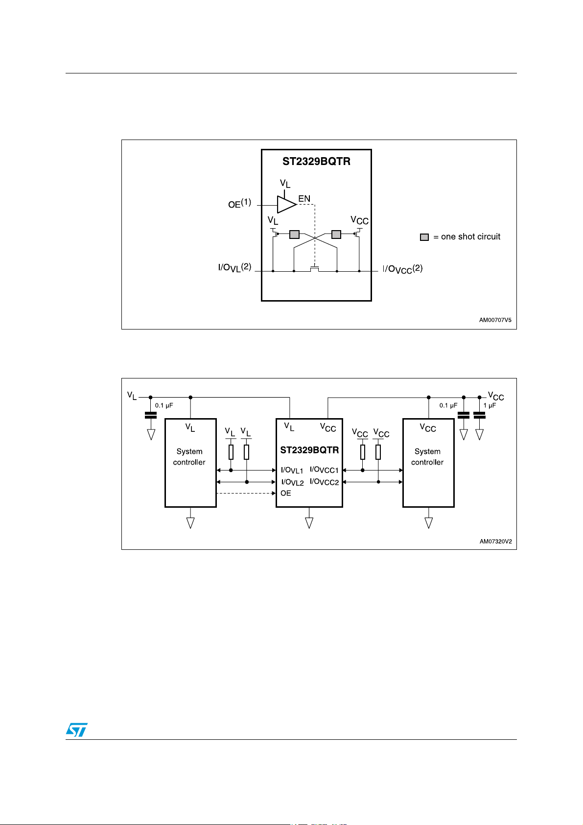
ST2329B Device block diagrams
3 Device block diagrams
Figure 2. ST2329BQTR block diagram
1. When OE is LOW, all I/Os are in high-impedance mode.
2. The ST2329BQTR has 2 channels. For simplicity, the diagram above shows only 1 channel.
Figure 3. Application block diagram
Doc ID 023359 Rev 1 7/22
 Loading...