

5 V powered multi-channel RS-232 drivers and receivers
Features
■ Supply voltage range: 4.5 to 5.5 V
■ Supply current no load (typ.): 1.5 mA
■ Transmitter output voltage swing (Typ): ± 9 V
■ Transition slew rate (typ.): 12 V/ms
■ Receiver propagation delay (typ.): 0.1 ms
■ Compatible with MAX202
■ Receiver input voltage range: ± 30 V
■ Data rate (typ.): 400 kbps/s
■ Operating temperature range:
-40 to 85 °C, 0 to 70 °C
SOP
ST202B
ST202C
SOP Large
TSSOP
Description
The ST202 is a 2 driver, 2 receiver device
following EIA/TIA-232 and V.28 communication
standard. It is particularly suitable for applications
where ± 12 V is not available. The ST202 uses a
single 5 V power supply and only four external
capacitors (0.1 µF). Typical application are in:
portable computers, low power modems,
interfaces translation, battery powered RS-232
networks.
Table 1. Device summary
Order code Temperature range Package Packaging
ST202BD -40 to 85 °C SO-16 (tube) 50 parts per tube / 20 tube per box
ST202CDR 0 to 70 °C SO-16 (tape and reel) 2500 parts per reel
ST202BDR -40 to 85 °C SO-16 (tape and reel) 2500 parts per reel
ST202CWR 0 to 70 °C SO-16 Large (tape and reel) 1000 parts per reel
ST202CTR 0 to 70 °C TSSOP16 (tape and reel) 2500 parts per reel
ST202BTR -40 to 85 °C TSSOP16 (tape and reel) 2500 parts per reel
February 2008 Rev 8 1/17
www.st.com
17

ST202B - ST202C
Contents
1 Pin configuration . . . . . . . . . . . . . . . . . . . . . . . . . . . . . . . . . . . . . . . . . . . 3
2 Maximum ratings . . . . . . . . . . . . . . . . . . . . . . . . . . . . . . . . . . . . . . . . . . . . 4
3 Electrical characteristics . . . . . . . . . . . . . . . . . . . . . . . . . . . . . . . . . . . . . 5
4 Typical application . . . . . . . . . . . . . . . . . . . . . . . . . . . . . . . . . . . . . . . . . . 7
5 Typical performance characteristics . . . . . . . . . . . . . . . . . . . . . . . . . . . . 8
6 Package mechanical data . . . . . . . . . . . . . . . . . . . . . . . . . . . . . . . . . . . . . 9
7 Revision history . . . . . . . . . . . . . . . . . . . . . . . . . . . . . . . . . . . . . . . . . . . 16
2/17
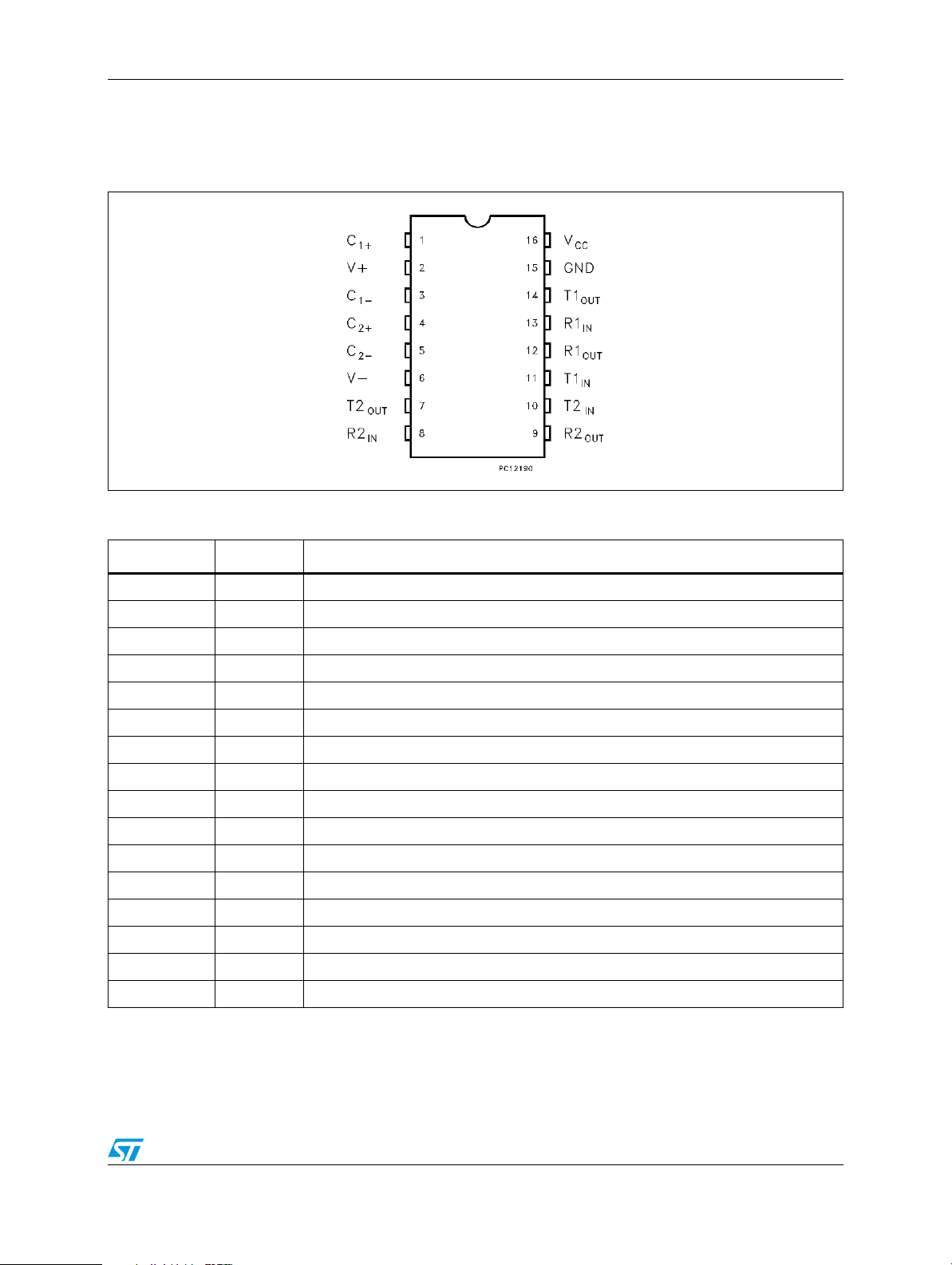
ST202B - ST202C Pin configuration
1 Pin configuration
Figure 1. Pin connections (top view)
Table 2. Pin description
Pin n° Symbol Note
1C
2 V+ Doubled voltage terminal
3C
4C
5C
6 V- Inverted voltage terminal
7T2
8R2
9R2
10 T2
11 T1
12 R1
13 R1
14 T1
15 GND Ground
16 V
+ Positive terminal for the first charge pump capacitor
1
- Negative terminal for the first charge pump capacitor
1
+ Positive terminal for the second charge pump capacitor
2
- Negative terminal for the second charge pump capacitor
2
OUT
OUT
OUT
OUT
CC
Second transmitter output voltage
Second receiver input voltage
IN
Second receiver output voltage
Second transmitter input voltage
IN
First transmitter input voltage
IN
First receiver output voltage
First receiver input voltage
IN
First transmitter output voltage
Supply voltage
3/17
Maximum ratings ST202B - ST202C
2 Maximum ratings
Table 3. Absolute maximum ratings
Symbol Parameter Value Unit
V
CC
V+ Extra positive voltage (V
Supply voltage -0.3 to 6 V
-0.3) to 13.2 V
CC
V- Extra negative voltage 0.3 to -13.2 V
T
R
T
OUT
R
OUT
T
SCTOUT
IN
IN
Transmitter input voltage range -0.3 to (VCC + 0.3) V
Receiver input voltage range ± 30 V
Transmitter output voltage range ± 15 V
Receiver output voltage range -0.3 to (VCC + 0.3) V
Short circuit duration on T
OUT
infinite
Note: Absolute maximum ratings are those values beyond which damage to the device may occur.
Functional operation under these condition is not implied.
4/17
ST202B - ST202C Electrical characteristics
3 Electrical characteristics
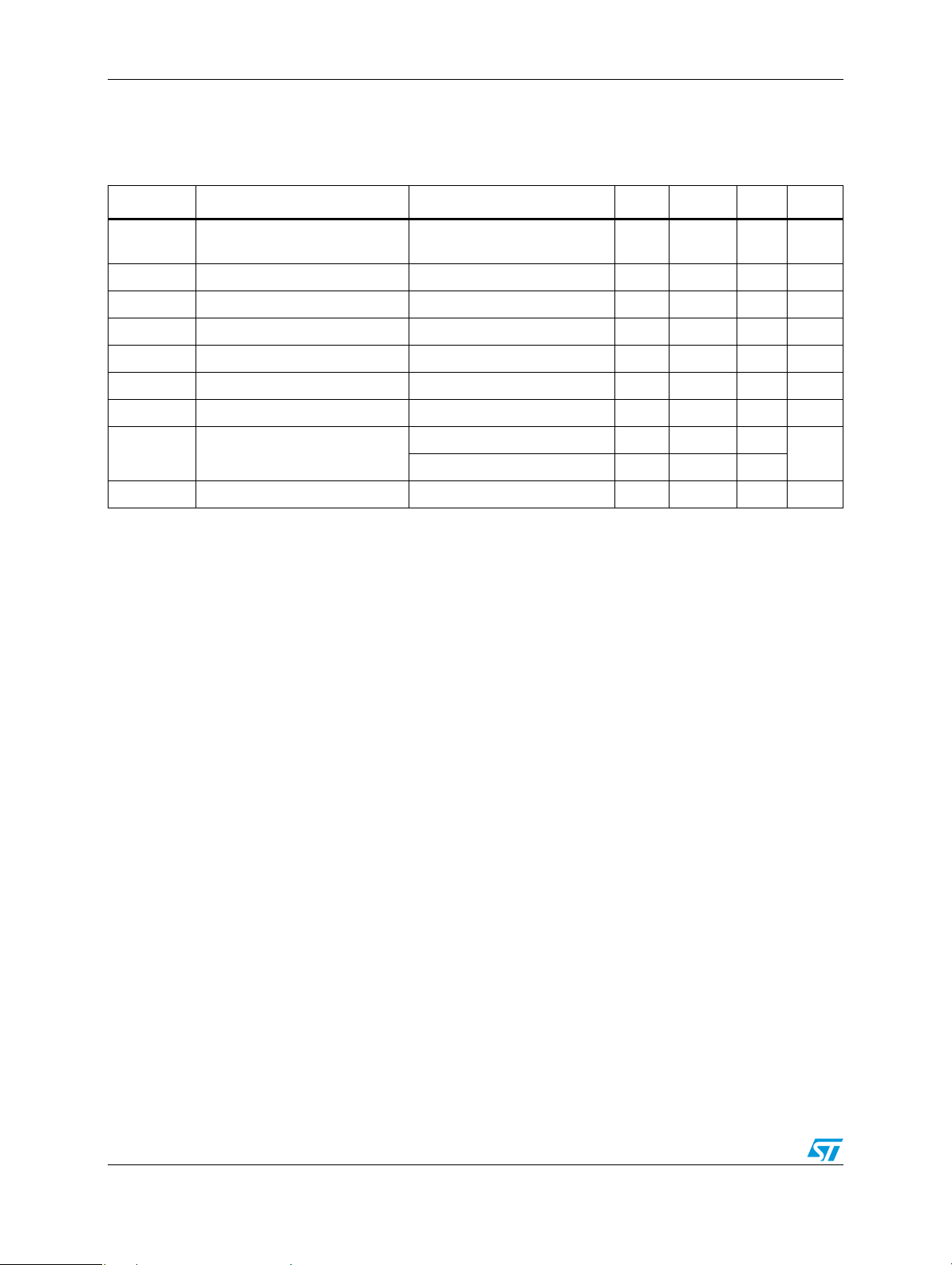
Table 4. Electrical characteristics
(C
- C4 = 0.1 µF, VCC = 5 V ± 10 %, TA = -40 to 85 °C, unless otherwise specified. Typical
1
values are referred to T
Symbol Parameter Test condition Min. Typ. Max. Unit
= 25 °C).
A
I
SUPPLY
VCC power supply current No Load 1.5 4 mA
Table 5. Transmitter electrical characteristics
(C
- C4 = 0.1 µF, VCC = 5 V ± 10 %, TA = -40 to 85 °C, unless otherwise specified. Typical
1
values are referred to T
Symbol Parameter Test condition Min. Typ. Max. Unit
V
TOUT
I
V
V
SR
D
R
TOUT
I
t
1. Measured from 3 V to -3 V or from -3 V to 3 V
2. One transmitter output is loaded with R
Output voltage swing
Logic pull-up current TIN = 0V 5 40 µA
TIL
Input logic threshold low 0.8 1.4 V
TIL
Input logic threshold high 1.4 2 V
TIH
Transition slew rate
T
Data rate
R
Transmitter output resistance VCC = V+ = V- = 0V V
Transmitter output short circuit
SC
current
Propagation delay time
DT
= 25 °C).
A
All transmitter outputs are loaded
with 3kΩ to GND
= 25°C, VCC = 5V
T
A
RL = 3 to 7kΩ, CL = 50 to 2500pF
(2)
One T
to GND ± 7 ± 22 mA
XOUT
TTL-CMOS IN to RS-232 OUT
= 150pF (50% to 50%)
C
L
= 3 kΩ to 7 kΩ, CL = 50 to 1000 pF
L
± 5 ± 9V
(1)
61230V/µs
200 400 kbits/s
= ± 2V 300 Ω
OUT
1.3 3.5 µs
5/17
Electrical characteristics ST202B - ST202C
Table 6. Receiver electrical characteristics
(C
- C4 = 0.1 µF, VCC = 5 V ± 10 %, TA = -40 to 85 °C, unless otherwise specified. Typical
1
values are referred to T
Symbol Parameter Test condition Min. Typ. Max. Unit
= 25 °C).
A
V
RIN
R
RIN
V
RIL
V
RIH
V
RIHYS
V
ROL
V
ROH
I
SCR
t
DR
1. RS-232 in to TTL-CMOS out (from 50% to 50%)
Receiver input voltage
operating range
RS-232 input resistance TA = 25°C 3 5 7 kΩ
RS-232 input threshold low 0.8 1.3 V
RS-232 input threshold high 1.8 2.4 V
RS-232 input hysteresis VCC = 5V 0.2 0.5 1 V
TTL/CMOS output voltage low I
TTL/CMOS output voltage high I
Receiver output short circuit
current
Propagation delay time CL = 150pF
-30 30 V
= 3.2mA (to VCC)0.20.4V
OUT
= 1mA (to GND) 3.5 VCC-0.2 V
OUT
to GND 2 10
mA
to V
CC
(1)
10 30
0.1 0.5 µs
6/17
 Loading...