

5 V powered multi-channel RS-232 drivers and receivers
Features
■ Supply voltage range: 4.5 to 5.5 V
■ Supply current no load (typ.): 1.5 mA
■ Transmitter output voltage swing (Typ): ± 9 V
■ Transition slew rate (typ.): 12 V/ms
■ Receiver propagation delay (typ.): 0.1 ms
■ Compatible with MAX202
■ Receiver input voltage range: ± 30 V
■ Data rate (typ.): 400 kbps/s
■ Operating temperature range:
-40 to 85 °C, 0 to 70 °C
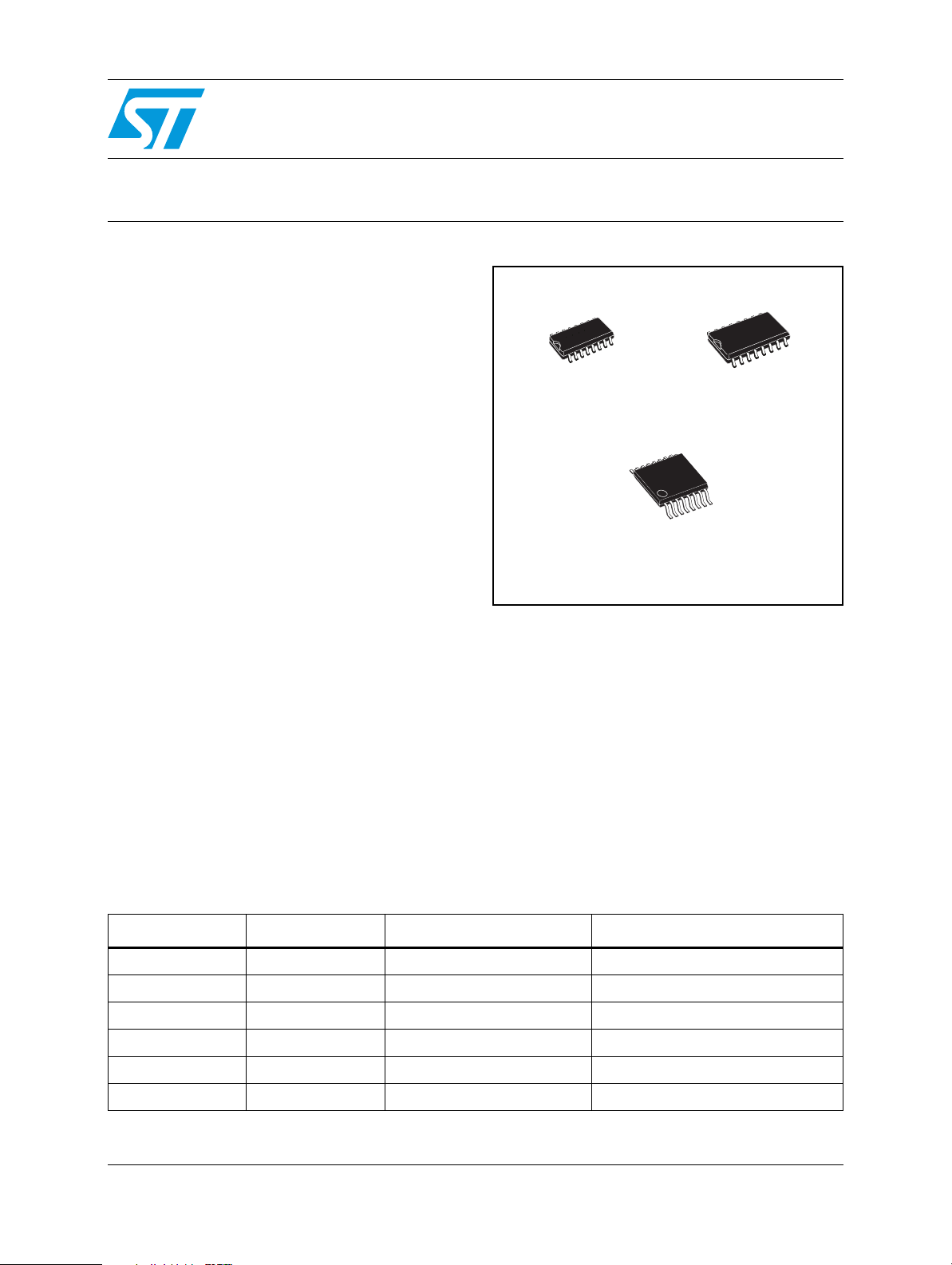
SOP
ST202B
ST202C
SOP Large
TSSOP
Description
The ST202 is a 2 driver, 2 receiver device
following EIA/TIA-232 and V.28 communication
standard. It is particularly suitable for applications
where ± 12 V is not available. The ST202 uses a
single 5 V power supply and only four external
capacitors (0.1 µF). Typical application are in:
portable computers, low power modems,
interfaces translation, battery powered RS-232
networks.
Table 1. Device summary
Order code Temperature range Package Packaging
ST202BD -40 to 85 °C SO-16 (tube) 50 parts per tube / 20 tube per box
ST202CDR 0 to 70 °C SO-16 (tape and reel) 2500 parts per reel
ST202BDR -40 to 85 °C SO-16 (tape and reel) 2500 parts per reel
ST202CWR 0 to 70 °C SO-16 Large (tape and reel) 1000 parts per reel
ST202CTR 0 to 70 °C TSSOP16 (tape and reel) 2500 parts per reel
ST202BTR -40 to 85 °C TSSOP16 (tape and reel) 2500 parts per reel
February 2008 Rev 8 1/17
www.st.com
17

ST202B - ST202C
Contents
1 Pin configuration . . . . . . . . . . . . . . . . . . . . . . . . . . . . . . . . . . . . . . . . . . . 3
2 Maximum ratings . . . . . . . . . . . . . . . . . . . . . . . . . . . . . . . . . . . . . . . . . . . . 4
3 Electrical characteristics . . . . . . . . . . . . . . . . . . . . . . . . . . . . . . . . . . . . . 5
4 Typical application . . . . . . . . . . . . . . . . . . . . . . . . . . . . . . . . . . . . . . . . . . 7
5 Typical performance characteristics . . . . . . . . . . . . . . . . . . . . . . . . . . . . 8
6 Package mechanical data . . . . . . . . . . . . . . . . . . . . . . . . . . . . . . . . . . . . . 9
7 Revision history . . . . . . . . . . . . . . . . . . . . . . . . . . . . . . . . . . . . . . . . . . . 16
2/17
ST202B - ST202C Pin configuration
1 Pin configuration
Figure 1. Pin connections (top view)
Table 2. Pin description
Pin n° Symbol Note
1C
2 V+ Doubled voltage terminal
3C
4C
5C
6 V- Inverted voltage terminal
7T2
8R2
9R2
10 T2
11 T1
12 R1
13 R1
14 T1
15 GND Ground
16 V
+ Positive terminal for the first charge pump capacitor
1
- Negative terminal for the first charge pump capacitor
1
+ Positive terminal for the second charge pump capacitor
2
- Negative terminal for the second charge pump capacitor
2
OUT
OUT
OUT
OUT
CC
Second transmitter output voltage
Second receiver input voltage
IN
Second receiver output voltage
Second transmitter input voltage
IN
First transmitter input voltage
IN
First receiver output voltage
First receiver input voltage
IN
First transmitter output voltage
Supply voltage
3/17
Maximum ratings ST202B - ST202C
2 Maximum ratings
Table 3. Absolute maximum ratings
Symbol Parameter Value Unit
V
CC
V+ Extra positive voltage (V
Supply voltage -0.3 to 6 V
-0.3) to 13.2 V
CC
V- Extra negative voltage 0.3 to -13.2 V
T
R
T
OUT
R
OUT
T
SCTOUT
IN
IN
Transmitter input voltage range -0.3 to (VCC + 0.3) V
Receiver input voltage range ± 30 V
Transmitter output voltage range ± 15 V
Receiver output voltage range -0.3 to (VCC + 0.3) V
Short circuit duration on T
OUT
infinite
Note: Absolute maximum ratings are those values beyond which damage to the device may occur.
Functional operation under these condition is not implied.
4/17
ST202B - ST202C Electrical characteristics
3 Electrical characteristics
Table 4. Electrical characteristics
(C
- C4 = 0.1 µF, VCC = 5 V ± 10 %, TA = -40 to 85 °C, unless otherwise specified. Typical
1
values are referred to T
Symbol Parameter Test condition Min. Typ. Max. Unit
= 25 °C).
A
I
SUPPLY
VCC power supply current No Load 1.5 4 mA
Table 5. Transmitter electrical characteristics
(C
- C4 = 0.1 µF, VCC = 5 V ± 10 %, TA = -40 to 85 °C, unless otherwise specified. Typical
1
values are referred to T
Symbol Parameter Test condition Min. Typ. Max. Unit
V
TOUT
I
V
V
SR
D
R
TOUT
I
t
1. Measured from 3 V to -3 V or from -3 V to 3 V
2. One transmitter output is loaded with R
Output voltage swing
Logic pull-up current TIN = 0V 5 40 µA
TIL
Input logic threshold low 0.8 1.4 V
TIL
Input logic threshold high 1.4 2 V
TIH
Transition slew rate
T
Data rate
R
Transmitter output resistance VCC = V+ = V- = 0V V
Transmitter output short circuit
SC
current
Propagation delay time
DT
= 25 °C).
A
All transmitter outputs are loaded
with 3kΩ to GND
= 25°C, VCC = 5V
T
A
RL = 3 to 7kΩ, CL = 50 to 2500pF
(2)
One T
to GND ± 7 ± 22 mA
XOUT
TTL-CMOS IN to RS-232 OUT
= 150pF (50% to 50%)
C
L
= 3 kΩ to 7 kΩ, CL = 50 to 1000 pF
L
± 5 ± 9V
(1)
61230V/µs
200 400 kbits/s
= ± 2V 300 Ω
OUT
1.3 3.5 µs
5/17
Electrical characteristics ST202B - ST202C
Table 6. Receiver electrical characteristics
(C
- C4 = 0.1 µF, VCC = 5 V ± 10 %, TA = -40 to 85 °C, unless otherwise specified. Typical
1
values are referred to T
Symbol Parameter Test condition Min. Typ. Max. Unit
= 25 °C).
A
V
RIN
R
RIN
V
RIL
V
RIH
V
RIHYS
V
ROL
V
ROH
I
SCR
t
DR
1. RS-232 in to TTL-CMOS out (from 50% to 50%)
Receiver input voltage
operating range
RS-232 input resistance TA = 25°C 3 5 7 kΩ
RS-232 input threshold low 0.8 1.3 V
RS-232 input threshold high 1.8 2.4 V
RS-232 input hysteresis VCC = 5V 0.2 0.5 1 V
TTL/CMOS output voltage low I
TTL/CMOS output voltage high I
Receiver output short circuit
current
Propagation delay time CL = 150pF
-30 30 V
= 3.2mA (to VCC)0.20.4V
OUT
= 1mA (to GND) 3.5 VCC-0.2 V
OUT
to GND 2 10
mA
to V
CC
(1)
10 30
0.1 0.5 µs
6/17

ST202B - ST202C Typical application
4 Typical application
Figure 2. Application circuit
(1) (2)
1. C
capacitors can even be 1µF ones
1-4
can be common or biased capacitors
2. C
1-4
Table 7. Capacitance value (µF)
C1 C2 C3 C4 C5
0.1 0.1 0.1 0.1 0.1
7/17

Typical performance characteristics ST202B - ST202C
5 Typical performance characteristics
(Unless otherwise specified TJ = 25 °C)
Figure 3. Driver voltage transfer
characteristics
Figure 4. Drive short circuit output current vs
temperature
Figure 5. Receiver threshold vs supply
voltage
Figure 7. Driver short circuit supply current
vs. temperature
Figure 6. Driver output capability current vs
output voltage
Figure 8. Receiver threshold vs temperature
8/17

ST202B - ST202C Package mechanical data
6 Package mechanical data
In order to meet environmental requirements, ST offers these devices in ECOPACK
packages. These packages have a lead-free second level interconnect. The category of
second Level Interconnect is marked on the package and on the inner box label, in
compliance with JEDEC Standard JESD97. The maximum ratings related to soldering
conditions are also marked on the inner box label. ECOPACK is an ST trademark.
ECOPACK specifications are available at: www.st.com.
®
9/17

Package mechanical data ST202B - ST202C
SO-16 mechanical data
Dim.
A 1.75 0.068
a1 0.1 0.25 0.004 0.010
a2 1.64 0.063
b 0.35 0.46 0.013 0.018
b1 0.19 0.25 0.007 0.010
C 0.5 0.019
c1 45° (typ.)
D 9.8 10 0.3850.393
E5.8 6.2 0.228 0.244
e 1.27 0.050
e38.89 0.350
F 3.8 4.0 0.149 0.157
G 4.6 5.3 0.181 0.208
L 0.5 1.27 0.019 0.050
M 0.62 0.024
S8° (max.)
Min. Typ. Max. Min. Typ. Max.
mm. inch.
10/17
0016020D

ST202B - ST202C Package mechanical data
SO-16L mechanical data
Dim.
A 2.65 0.104
a1 0.1 0.2 0.004 0.008
a2 2.45 0.096
b 0.350.49 0.014 0.019
b1 0.23 0.32 0.009 0.012
C 0.5 0.020
c1 45° (typ.)
D 10.1 10.5 0.397 0.413
E 10.0 10.65 0.393 0.419
e 1.27 0.050
e38.89 0.350
F 7.4 7.6 0.2910.300
G
L 0.5 1.27 0.020 0.050
M 0.75 0.029
S8° (max.)
Min. Typ. Max. Min. Typ. Max.
mm. inch.
PO13I
11/17

Package mechanical data ST202B - ST202C
TSSOP16 mechanical data
mm. inch.
Dim.
Min. Typ. Max. Min. Typ. Max.
A 1.2 0.047
A1 0.05 0.15 0.002 0.004 0.006
A2 0.8 1 1.05 0.031 0.039 0.041
b 0.19 0.30 0.007 0.012
c0.09 0.20 0.004 0.0079
D4.9 5 5.1 0.193 0.197 0.201
E 6.2 6.4 6.6 0.244 0.252 0.260
E1 4.3 4.4 4.48 0.169 0.173 0.176
e 0.65 BSC 0.0256 BSC
K0° 8°0° 8°
L 0.45 0.60 0.75 0.018 0.024 0.030
A2
A
A1
b
e
c
K
L
E
D
E1
PIN 1 IDENTIFICATION
12/17
1
0080338D

ST202B - ST202C Package mechanical data
Tape & reel SO-16 mechanical data
mm. inch.
Dim.
Min. Typ. Max. Min. Typ. Max.
A 330 12.992
C 12.8 13.2 0.504 0.519
D 20.2 0.795
N60 2.362
T 22.4 0.882
Ao 6.45 6.65 0.254 0.262
Bo 10.3 10.5 0.406 0.414
Ko 2.1 2.3 0.082 0.090
Po 3.9 4.1 0.153 0.161
P7.98.1 0.311 0.319
13/17

Package mechanical data ST202B - ST202C
Tape & reel SO-16L mechanical data
mm. inch.
Dim.
Min. Typ. Max. Min. Typ. Max.
A 330 12.992
C 12.8 13.2 0.504 0.519
D 20.2 0.795
N60 2.362
T 22.4 0.882
Ao 10.8 11.0 0.425 0.433
Bo 10.7 10.9 0.421 0.429
Ko 2.93.1 0.114 0.122
Po 3.9 4.1 0.153 0.161
P 11.9 12.1 0.468 0.476
14/17

ST202B - ST202C Package mechanical data
Tape & reel TSSOP16 mechanical data
mm. inch.
Dim.
Min. Typ. Max. Min. Typ. Max.
A 330 12.992
C 12.8 13.2 0.504 0.519
D 20.2 0.795
N60 2.362
T 22.4 0.882
Ao 6.7 6.9 0.264 0.272
Bo 5.3 5.5 0.209 0.217
Ko 1.6 1.8 0.063 0.071
Po 3.9 4.1 0.153 0.161
P7.98.1 0.311 0.319
15/17

Revision history ST202B - ST202C
7 Revision history
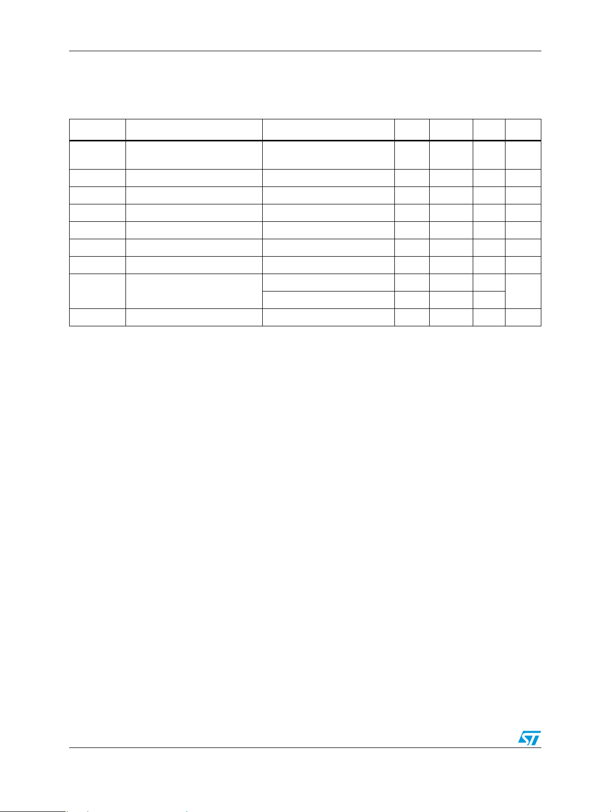
Table 8. Document revision history
Date Revision Changes
09-Mar-2006 5 Order codes updated and the document has been reformatted.
16-Jul-2007 6 Device summary updated.
14-Nov-2007 7 Modified: Ta b le 1 .
11-Feb-2008 8 Modified: Table 1 on page 1.
16/17

ST202B - ST202C
Please Read Carefully:
Information in this document is provided solely in connection with ST products. STMicroelectronics NV and its subsidiaries (“ST”) reserve the
right to make changes, corrections, modifications or improvements, to this document, and the products and services described herein at any
time, without notice.
All ST products are sold pursuant to ST’s terms and conditions of sale.
Purchasers are solely responsible for the choice, selection and use of the ST products and services described herein, and ST assumes no
liability whatsoever relating to the choice, selection or use of the ST products and services described herein.
No license, express or implied, by estoppel or otherwise, to any intellectual property rights is granted under this document. If any part of this
document refers to any third party products or services it shall not be deemed a license grant by ST for the use of such third party products
or services, or any intellectual property contained therein or considered as a warranty covering the use in any manner whatsoever of such
third party products or services or any intellectual property contained therein.
UNLESS OTHERWISE SET FORTH IN ST’S TERMS AND CONDITIONS OF SALE ST DISCLAIMS ANY EXPRESS OR IMPLIED
WARRANTY WITH RESPECT TO THE USE AND/OR SALE OF ST PRODUCTS INCLUDING WITHOUT LIMITATION IMPLIED
WARRANTIES OF MERCHANTABILITY, FITNESS FOR A PARTICULAR PURPOSE (AND THEIR EQUIVALENTS UNDER THE LAWS
OF ANY JURISDICTION), OR INFRINGEMENT OF ANY PATENT, COPYRIGHT OR OTHER INTELLECTUAL PROPERTY RIGHT.
UNLESS EXPRESSLY APPROVED IN WRITING BY AN AUTHORIZED ST REPRESENTATIVE, ST PRODUCTS ARE NOT
RECOMMENDED, AUTHORIZED OR WARRANTED FOR USE IN MILITARY, AIR CRAFT, SPACE, LIFE SAVING, OR LIFE SUSTAINING
APPLICATIONS, NOR IN PRODUCTS OR SYSTEMS WHERE FAILURE OR MALFUNCTION MAY RESULT IN PERSONAL INJURY,
DEATH, OR SEVERE PROPERTY OR ENVIRONMENTAL DAMAGE. ST PRODUCTS WHICH ARE NOT SPECIFIED AS "AUTOMOTIVE
GRADE" MAY ONLY BE USED IN AUTOMOTIVE APPLICATIONS AT USER’S OWN RISK.
Resale of ST products with provisions different from the statements and/or technical features set forth in this document shall immediately void
any warranty granted by ST for the ST product or service described herein and shall not create or extend in any manner whatsoever, any
liability of ST.
ST and the ST logo are trademarks or registered trademarks of ST in various countries.
Information in this document supersedes and replaces all information previously supplied.
The ST logo is a registered trademark of STMicroelectronics. All other names are the property of their respective owners.
© 2008 STMicroelectronics - All rights reserved
STMicroelectronics group of companies
Australia - Belgium - Brazil - Canada - China - Czech Republic - Finland - France - Germany - Hong Kong - India - Israel - Italy - Japan -
Malaysia - Malta - Morocco - Singapore - Spain - Sweden - Switzerland - United Kingdom - United States of America
www.st.com
17/17
 Loading...