

ST ST1S40 User Manual
3 A DC step-down switching regulator
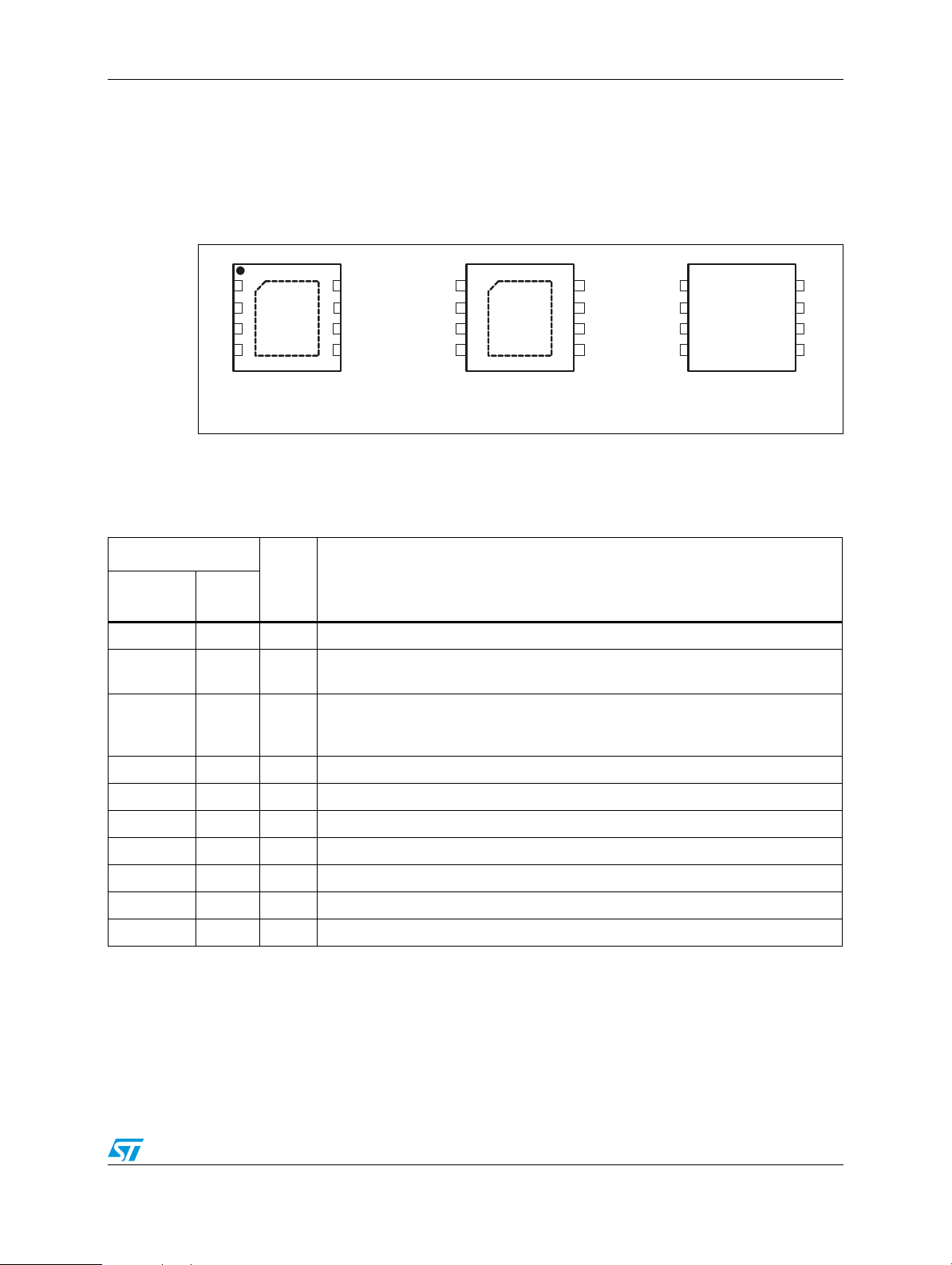
VFQFPN 4x4SO8
9,16:
6:
)%
3*1'$*1'H3DG
(13*
676,
&LQBVZ
)
&RXW
)
/+
5
5
9,1$
&LQBD
± )
92879
9,1 9
Features
■ 3 A DC output current
■ 4.0 V to 18 V input voltage
■ Output voltage adjustable from 0.8 V
■ 850 kHz switching frequency
■ Internal soft-start
■ Integrated 95 mΩ and 69 mΩ Power MOSFETs
■ All ceramic capacitor
■ Enable
■ Cycle-by-cycle current limiting
■ Current fold back short-circuit protection
■ VFQFPN4x4-8L, HSOP-8, and SO-8 and
packages
Applications
■ μP/ASIC/DSP/FPGA core and I/O supplies
■ Point of load for: STB, TVs, DVD
■ Optical storage, hard disk drive, printers,
audio/graphic cards
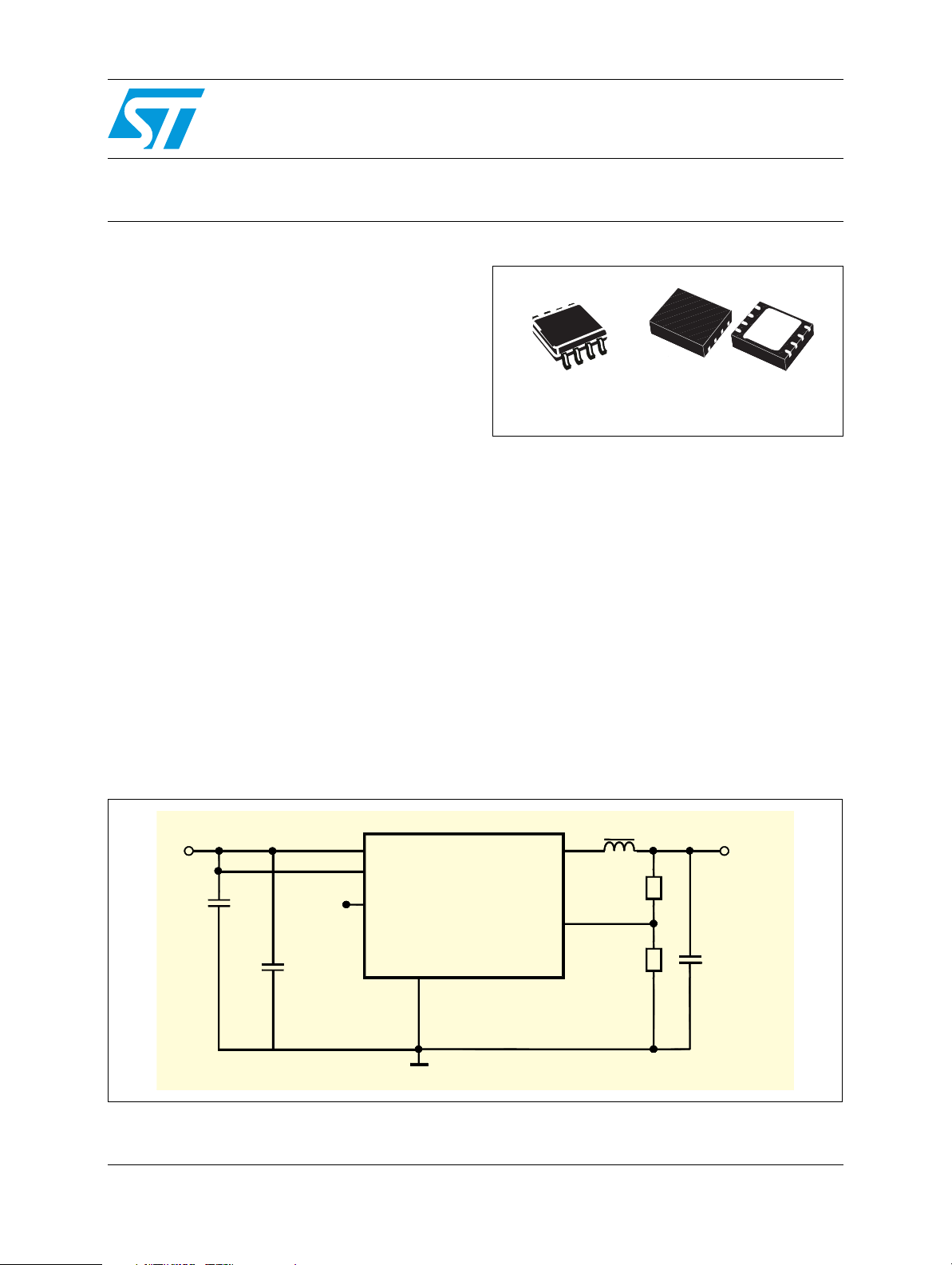
Figure 1. Application circuit
ST1S40
Description
The ST1S40 is an internally compensated 850
kHz fixed-frequency PWM synchronous stepdown regulator. ST1S40 operates from 4.0 V to
18 V input, while it regulates an output voltage as
low as 0.8 V and up to V
The ST1S40 integrates a 95 mΩ high side switch
and 69 mΩ synchronous rectifier allowing very
high efficiency with very low output voltages.
The peak current mode control with internal
compensation delivers a very compact solution
with a minimum component count.
The ST1S40 is available in VFQFPN 4 mm x 4
mm 8 lead package, HSOP-8 and standard SO-8.
.
IN
March 2012 Doc ID 17928 Rev 4 1/30
www.st.com
30

Contents ST1S40
Contents
1 Pin settings . . . . . . . . . . . . . . . . . . . . . . . . . . . . . . . . . . . . . . . . . . . . . . . . 3
1.1 Pin connection . . . . . . . . . . . . . . . . . . . . . . . . . . . . . . . . . . . . . . . . . . . . . . 3
1.2 Pin description . . . . . . . . . . . . . . . . . . . . . . . . . . . . . . . . . . . . . . . . . . . . . . 3
2 Maximum ratings . . . . . . . . . . . . . . . . . . . . . . . . . . . . . . . . . . . . . . . . . . . . 4
3 Thermal data . . . . . . . . . . . . . . . . . . . . . . . . . . . . . . . . . . . . . . . . . . . . . . . 4
4 Electrical characteristics . . . . . . . . . . . . . . . . . . . . . . . . . . . . . . . . . . . . . 5
5 Functional description . . . . . . . . . . . . . . . . . . . . . . . . . . . . . . . . . . . . . . . 7
5.1 Internal soft-start . . . . . . . . . . . . . . . . . . . . . . . . . . . . . . . . . . . . . . . . . . . . 8
5.2 Error amplifier and control loop stability . . . . . . . . . . . . . . . . . . . . . . . . . . . 8
5.3 Overcurrent protection . . . . . . . . . . . . . . . . . . . . . . . . . . . . . . . . . . . . . . . 12
5.4 Enable function . . . . . . . . . . . . . . . . . . . . . . . . . . . . . . . . . . . . . . . . . . . . . 13
5.5 Hysteretic thermal shutdown . . . . . . . . . . . . . . . . . . . . . . . . . . . . . . . . . . 13
6 Application information . . . . . . . . . . . . . . . . . . . . . . . . . . . . . . . . . . . . . 14
6.1 Input capacitor selection . . . . . . . . . . . . . . . . . . . . . . . . . . . . . . . . . . . . . . 14
6.2 Inductor selection . . . . . . . . . . . . . . . . . . . . . . . . . . . . . . . . . . . . . . . . . . . 15
6.3 Output capacitor selection . . . . . . . . . . . . . . . . . . . . . . . . . . . . . . . . . . . . 16
6.4 Thermal dissipation . . . . . . . . . . . . . . . . . . . . . . . . . . . . . . . . . . . . . . . . . 17
6.5 Layout consideration . . . . . . . . . . . . . . . . . . . . . . . . . . . . . . . . . . . . . . . . 18
7 Demonstration board . . . . . . . . . . . . . . . . . . . . . . . . . . . . . . . . . . . . . . . 20
8 Typical characteristics . . . . . . . . . . . . . . . . . . . . . . . . . . . . . . . . . . . . . . 22
9 Package mechanical data . . . . . . . . . . . . . . . . . . . . . . . . . . . . . . . . . . . . 23
10 Order codes . . . . . . . . . . . . . . . . . . . . . . . . . . . . . . . . . . . . . . . . . . . . . . . 27
11 Revision history . . . . . . . . . . . . . . . . . . . . . . . . . . . . . . . . . . . . . . . . . . . 28
2/30 Doc ID 17928 Rev 4
ST1S40 Pin settings
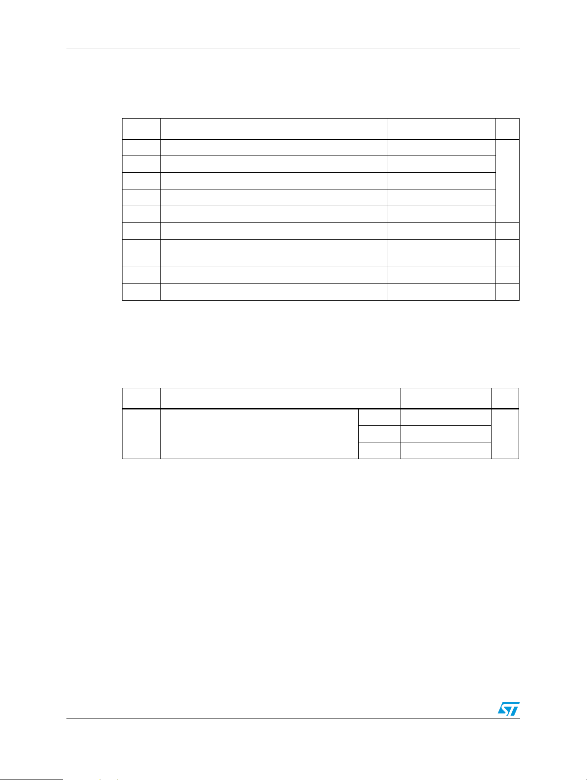
1 Pin settings
1.1 Pin connection
Figure 2. Pin connection (top view)
VINA
EN
FB
GND
1
2
9
3
4
PGND
8
SW
7
VINSW
6
NC
5
VFQFPN
1.2 Pin description
No.
S08-BW
Type Description
V
Unregulated DC input voltage
INA
Enable input. With EN higher than 1.2 V the device in ON and with EN lower than
0.4 V the device is OFF (ST1S40Ixx).
Feedback input. Connecting the output voltage directly to this pin the output
voltage is regulated at 0.8 V. To have higher regulated voltages an external
resistor divider is required from Vout to the FB pin.
Table 1. Pin description
VFQFPN
and HSOP8
13
24EN
35FB
4 6 AGND Ground
5 - NC It can be connected to ground
VINA
EN
FB
GND
1
2
9
3
4
PGND
8
SW
7
VINSW
6
NC
5
1
SW VINSW
PGND
VINA
EN
45
HSOP8SO8-BW
8
GND
AGND
FB
6 8 VINSW Power input voltage
7 1 SW Regulator output switching pin
8 2 PGND Power ground
- 7 Ground
9 - ePad Exposed pad mandatory connected to ground
Doc ID 17928 Rev 4 3/30
Maximum ratings ST1S40
2 Maximum ratings
Table 2. Absolute maximum ratings
Symbol Parameter Value Unit
V
V
V
V
V
P
T
T
Power input voltage -0.3 to 20
INSW
Input voltage -0.3 to 20
INA
Enable voltage -0.3 to V
EN
Output switching voltage -1 to V
SW
Feedback voltage -0.3 to 2.5
FB
I
FB current -1 to +1 mA
FB
Power dissipation at TA < 60 °C
TOT
Operating junction temperature range -40 to 150 °C
OP
Storage temperature range -55 to 150 °C
stg
3 Thermal data
Table 3. Thermal data
Symbol Parameter Value Unit
R
Maximum thermal resistance junction-ambient
thJA
2.25 (HSOP8/DFN4x4);
VFQFPN 40
(1)
SO8-BW 55
INA
IN
1.6 SO8-BW
V
W
°C/WHSOP8 40
1. Package mounted on demonstration board.
4/30 Doc ID 17928 Rev 4
ST1S40 Electrical characteristics
4 Electrical characteristics
TJ=25 °C, VCC=12 V, unless otherwise specified.
Table 4. Electrical characteristics
Val ues
Symbol Parameter Test condition
Min. Typ. Max.
Unit
Operating input voltage
IN
range
Tur n-o n VCC threshold
Threshold hysteresis
High side switch ON
-P
resistance
Low side switch ON
-N
resistance
Maximum limiting current
V
R
R
V
V
INON
INHYS
DSON
DSON
I
LIM
Oscillator
D
F
SW
MAX
Switching frequency 0.7 0.85 1 MHz
Maximum duty cycle
Dynamic characteristics
%V
ΔI
%V
V
ΔV
FB
OUT
OUT
OUT
Feedback voltage
/
Reference load regulation Isw=10 mA to I
/
Reference line regulation VIN= 4.0 V to 18 V
IN
DC characteristics
(1)
(1)
(1)
ISW=750 mA
418
2.9
V
0.250
95
mΩ
ISW=750 mA 69 mΩ
(2)
(2)
4.0 6.0 A
100 %
0.784 0.8 0.816
(1)
LIM
0.776 0.8 0.824
(2)
(2)
0.5 %
0.4 %
V
I
Q
I
QST-BY
Quiescent current
Total standby quiescent
current
Duty cycle=0, no load
=1.2 V
V
FB
OFF 2 15 μA
IFB FB bias current 50
Enable
Device ON level 1.2
V
EN
I
EN
EN threshold voltage
Device OFF level 0.4
EN current 2 μA
Doc ID 17928 Rev 4 5/30
1.5 2.5 mA
V
Electrical characteristics ST1S40
Table 4. Electrical characteristics (continued)
Val ues
Symbol Parameter Test condition
Min. Typ. Max.
Soft start
Unit
T
SS
Soft-start duration 1 ms
Protection
Thermal shutdown 150
T
SHDN
1. Specification referred to TJ from -40 to +125 °C. Specifications in the -40 to +125 °C temperature range are
assured by design, characterization and statistical correlation.
2. Guaranteed by design.
Hysteresis 15
°C
6/30 Doc ID 17928 Rev 4
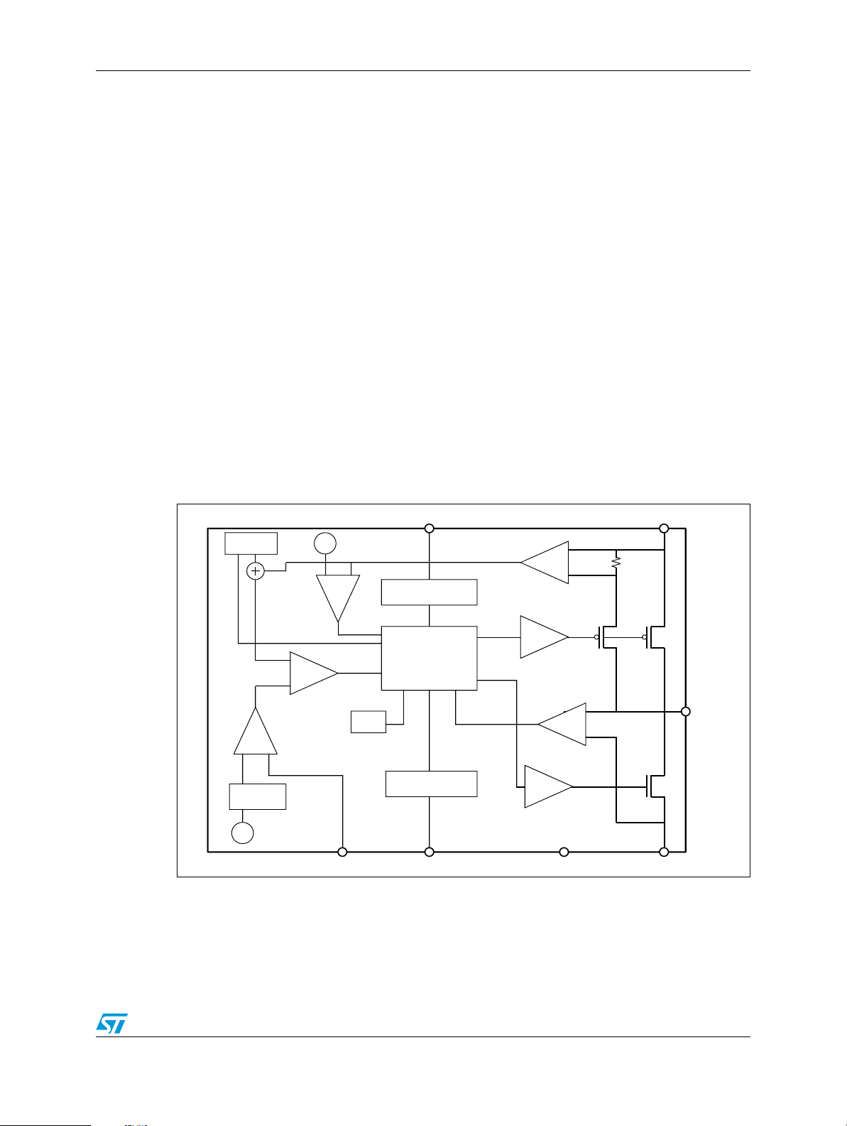
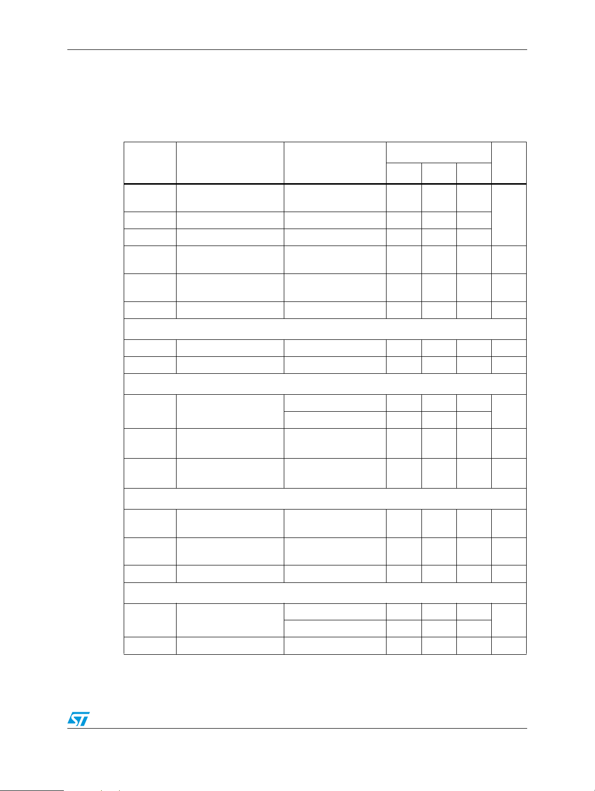
ST1S40 Functional description
OSC
E/A
DRIVER
DRIVER
DMD
OTP
MOSFET
CONTROL
LOGIC
REGULATOR
SHUT-DOWN
I_SENSE
COMP
COMP
OCP
REF
0.8V
SOFTSTART
Vsum
Vc
OCP
UVLO
Vdrv_p
Vdrv_n
I2V
R
SENSE
VINA VINSW
SW
GNDPGNDAENFB
5 Functional description
The ST1S40 is based on a “peak current mode”, constant frequency control. The output
voltage V
providing an error signal that, compared to the output of the current sense amplifier, controls
the ON and OFF time of the power switch.
The main internal blocks are shown in the block diagram in Figure 3. They are:
● A fully integrated oscillator that provides the internal clock and the ramp for the slope
compensation avoiding sub-harmonic instability
● The soft-start circuitry to limit inrush current during the startup phase
● The transconductance error amplifier with integrated compensation network
● The pulse width modulator and the relative logic circuitry necessary to drive the internal
power switches
● The drivers for embedded P-channel and N-channel Power MOSFET switches
● The high side current sensing block
● The low side current sense to implement diode emulation
● A voltage monitor circuitry (UVLO) that checks the input and internal voltages
● A thermal shutdown block, to prevent thermal run-away.
is sensed by the feedback pin (FB) compared to an internal reference (0.8 V)
OUT
Figure 3. Block diagram
5.1 Internal soft-start
The soft-start is essential to assure correct and safe startup of the step-down converter. It
avoids inrush current surge and causes the output voltage to increase monothonically.
Doc ID 17928 Rev 4 7/30
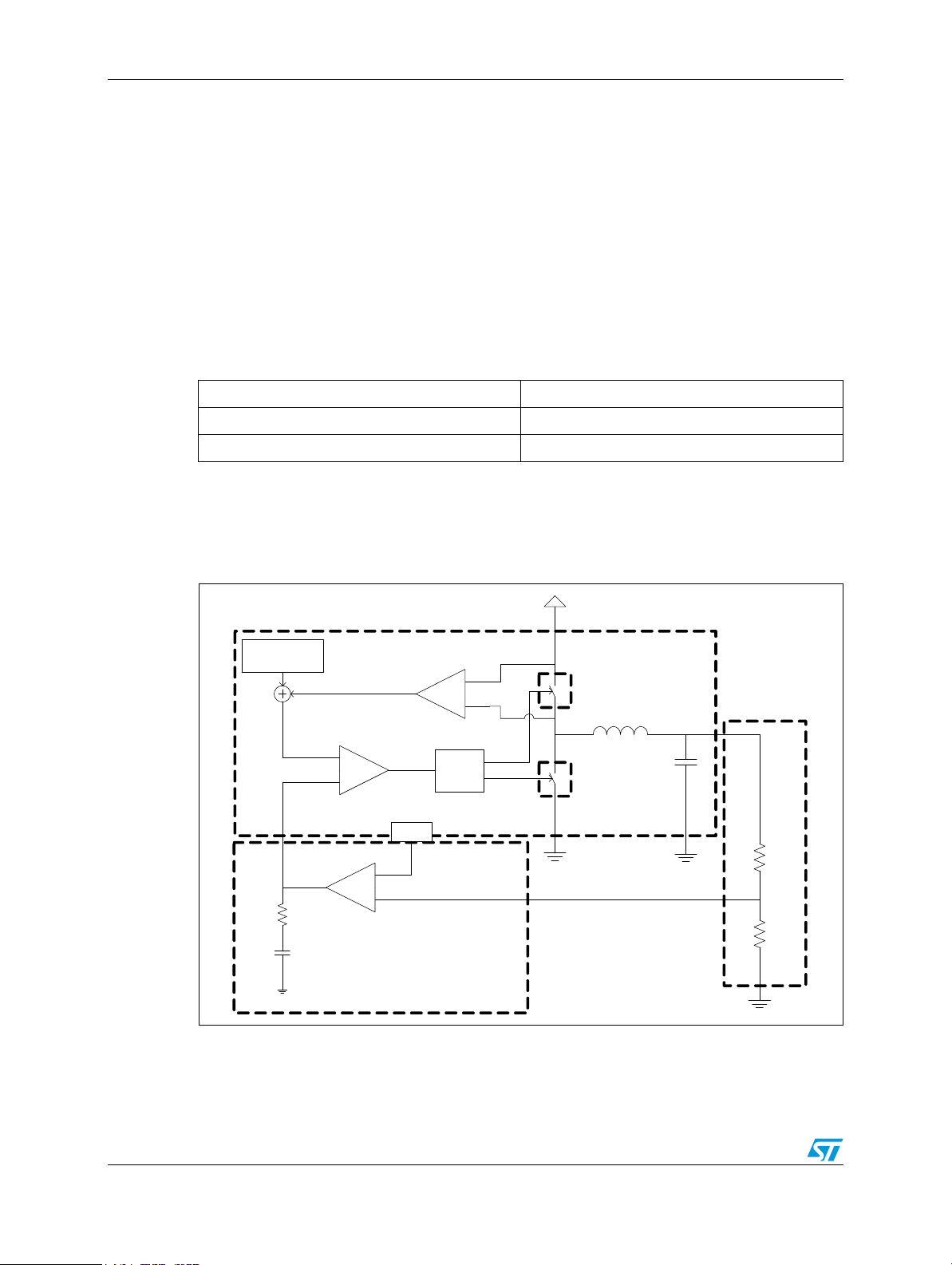
Functional description ST1S40
L
Cout
Cur rent s ense
Logic
And
Driver
Slope
Com pensati on
PW M comparator
Error Amp
Rc
Cc
R1
R2
0.8 V
Hi gh side
Swi tch
Low s i de
Swi tch
GCO(s)
G
DIV
(s)
G
EA
(s)
VIN
V
C
V
OUT
V
FB
The soft-start is performed by ramping the non-inverting input (V
from 0 V to 0.8 V in around 1 ms.
5.2 Error amplifier and control loop stability
The error amplifier compares the FB pin voltage with the internal 0.8 V reference and it
provides the error signal to be compared with the output of the current sense circuitry, that is
the high side Power MOSFET current. Comparing the output of the error amplifier and the
peak inductor current implements the peak current mode control loop.
The error amplifier is a transconductance amplifier (OTA). The uncompensated
characteristics are listed inTable 5.
Table 5. Error amplifier characteristics
DC Gain 95 dB
Gm 251 µA/V
Ro 240 MΩ
The ST1S40 embeds the compensation network that assures the stability of the loop in the
whole operating range. All the tools needed to check the loop stability are shown below.
Figure 4. shows the simple small signal model for the peak current mode control loop.
Figure 4. Block diagram of the loop for the small signal analysis
) of the error amplifier
REF
8/30 Doc ID 17928 Rev 4

ST1S40 Functional description
GCOs()
R
LOAD
R
i
----------------- -
1
1
R
outTSW
⋅
L
--------------------------- -
m
C
1D–()0,5–⋅[]⋅+
-------------------------------------------------------------------------------------------- -
1
s
ω
z
------+
1
s
ω
p
------+
--------------------- - FHs()⋅⋅⋅=
ω
Z
1
ESR C
OUT
⋅
-------------------------------=
ω
p
1
R
LOADCOUT
⋅
------------------------------------- -
m
C
1D–()0,5–⋅
LC
OUTfSW
⋅⋅
---------------------------------------------+=
mC1
S
e
S
n
------ +=
S
e
Vppf
SW
⋅=
S
n
VINV
OUT
–
L
----------------------------- -
Ri⋅=
FHs()
1
1
s
ω
nQP
⋅
------------------ -
s
2
ω
n
2
------++
------------------------------------------ -=
Three main terms can be identified to obtain the loop transfer function:
1. from control (output of E/A) to output, G
2. from output (Vout) to the FB pin, G
DIV
3. from the FB pin to control (output of E/A), G
The transfer function from control to output G
CO
(s)
CO
(s)
(s).
EA
(s) results:
Equation 1
where R
current sense circuitry, ω
represents the load resistance, Ri (0.3 Ω) the equivalent sensing resistor of the
LOAD
the single pole introduced by the LC filter and ωz the zero given by
p
the ESR of the output capacitor.
F
(s) accounts for the sampling effect performed by the PWM comparator on the output of
H
the error amplifier that introduces a double pole at one half of the switching frequency.
Equation 2
Equation 3
where:
Equation 4
S
represents the ON time slope of the sensed inductor current, Se the slope of the external
n
ramp (V
peak-to-peak amplitude 1.25 V) that implements the slope compensation to
PP
avoid sub-harmonic oscillations at duty cycle over 50%.
The sampling effect contribution F
(s) is:
H
Equation 5
where:
Doc ID 17928 Rev 4 9/30
 Loading...