

3 A DC step-down switching regulator
Features
■ 3 A DC output current
■ 2.8 V to 5.5 V input voltage
■ Output voltage adjustable from 0.8 V
■ 1.5 MHz switching frequency
■ Internal soft-start and enable
■ Integrated 60 mΩ and 45 mΩ Power MOSFETs
■ All ceramic capacitor
■ Power Good (POR)
■ Cycle-by-cycle current limiting
■ Current foldback short-circuit protection
■ VFDFPN3x3-8L, SO8 packages
Applications
■ µP/ASIC/DSP/FPGA core and I/O supplies
■ Point of load for: STB, TVs, DVDs
■ Optical storage, hard disk drive, printers,
audio/graphic cards
ST1S31
Datasheet − production data
SO8VFDFPN 3x3-8L
Description
The ST1S31 is an internally compensated 1.5
MHz fixed-frequency PWM synchronous stepdown regulator. The ST1S31 operates from 2.8 V
to 5.5 V input, while it regulates an output voltage
as low as 0.8 V and up to V
The ST1S31 integrates a 60 mΩ high-side switch
and 45 mΩ synchronous rectifier allowing very
high efficiency with very low output voltages.
The peak current mode control with internal
compensation delivers a very compact solution
with a minimum component count.
IN
.
The ST1S31 is available in 3 mm x 3 mm, 8 lead
VFDFPN and SO8 packages.
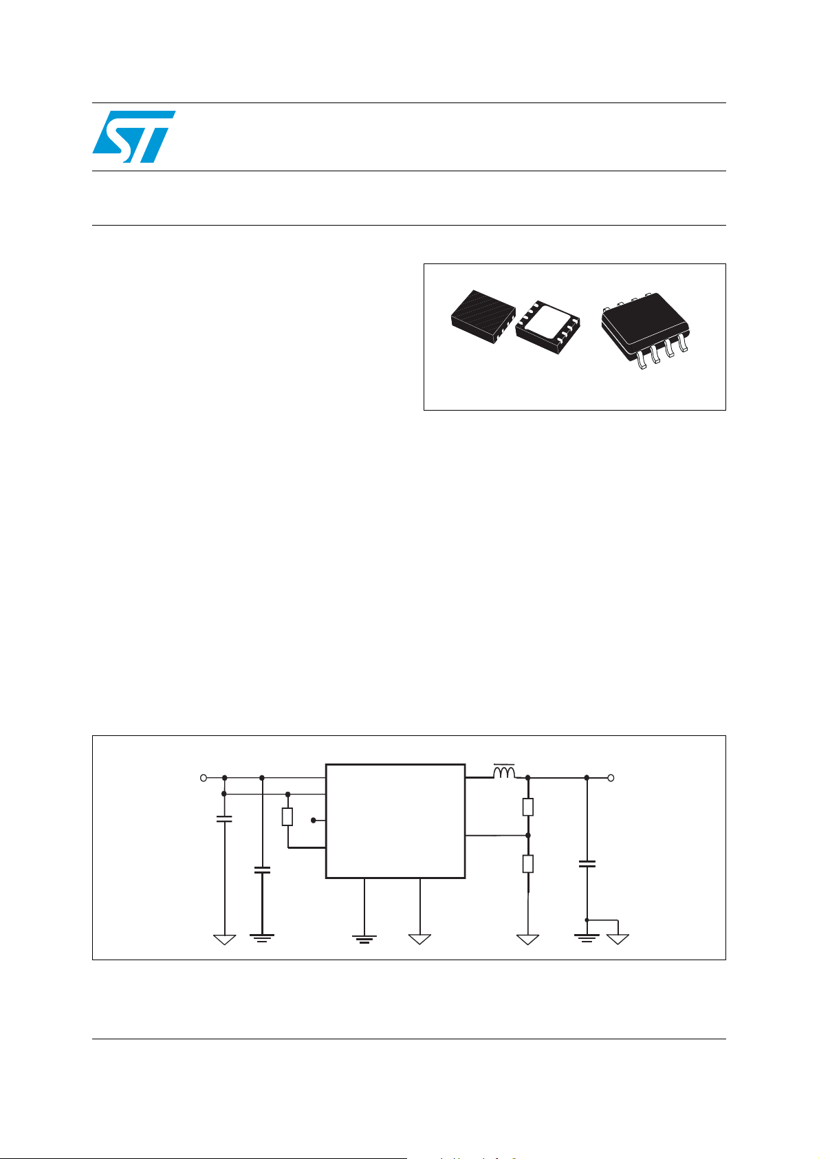
Figure 1. Application circuit
VIN
a
Cin_
Cin_sw
April 2012 Doc ID 022998 Rev 1 1/30
This is information on a product in full production.
R3
VINSW
VINA
EN
PG
GND
SW
ST1S31
VFB
ePAD
L
R1
R2
VOUT
Cout
AM11415v
www.st.com
30

Contents ST1S31
Contents
1 Pin settings . . . . . . . . . . . . . . . . . . . . . . . . . . . . . . . . . . . . . . . . . . . . . . . . 3
1.1 Pin connection . . . . . . . . . . . . . . . . . . . . . . . . . . . . . . . . . . . . . . . . . . . . . . 3
1.2 Pin description . . . . . . . . . . . . . . . . . . . . . . . . . . . . . . . . . . . . . . . . . . . . . . 3
2 Maximum ratings . . . . . . . . . . . . . . . . . . . . . . . . . . . . . . . . . . . . . . . . . . . . 4
2.1 Thermal data . . . . . . . . . . . . . . . . . . . . . . . . . . . . . . . . . . . . . . . . . . . . . . . 4
3 Electrical characteristics . . . . . . . . . . . . . . . . . . . . . . . . . . . . . . . . . . . . . 5
4 Functional description . . . . . . . . . . . . . . . . . . . . . . . . . . . . . . . . . . . . . . . 7
4.1 Soft-start . . . . . . . . . . . . . . . . . . . . . . . . . . . . . . . . . . . . . . . . . . . . . . . . . . . 8
4.2 Error amplifier and control loop stability . . . . . . . . . . . . . . . . . . . . . . . . . . . 8
4.3 Overcurrent protection . . . . . . . . . . . . . . . . . . . . . . . . . . . . . . . . . . . . . . . 13
4.4 Enable function . . . . . . . . . . . . . . . . . . . . . . . . . . . . . . . . . . . . . . . . . . . . . 14
4.5 Light load operation . . . . . . . . . . . . . . . . . . . . . . . . . . . . . . . . . . . . . . . . . 14
4.6 Hysteretic thermal shutdown . . . . . . . . . . . . . . . . . . . . . . . . . . . . . . . . . . 14
5 Application information . . . . . . . . . . . . . . . . . . . . . . . . . . . . . . . . . . . . . 15
5.1 Input capacitor selection . . . . . . . . . . . . . . . . . . . . . . . . . . . . . . . . . . . . . . 15
5.2 Inductor selection . . . . . . . . . . . . . . . . . . . . . . . . . . . . . . . . . . . . . . . . . . . 16
5.3 Output capacitor selection . . . . . . . . . . . . . . . . . . . . . . . . . . . . . . . . . . . . 17
5.4 Thermal dissipation . . . . . . . . . . . . . . . . . . . . . . . . . . . . . . . . . . . . . . . . . 18
5.5 Layout consideration . . . . . . . . . . . . . . . . . . . . . . . . . . . . . . . . . . . . . . . . 19
6 Demonstration board . . . . . . . . . . . . . . . . . . . . . . . . . . . . . . . . . . . . . . . 21
7 Typical characteristics . . . . . . . . . . . . . . . . . . . . . . . . . . . . . . . . . . . . . . 23
8 Package mechanical data . . . . . . . . . . . . . . . . . . . . . . . . . . . . . . . . . . . . 24
9 Order codes . . . . . . . . . . . . . . . . . . . . . . . . . . . . . . . . . . . . . . . . . . . . . . . 28
10 Revision history . . . . . . . . . . . . . . . . . . . . . . . . . . . . . . . . . . . . . . . . . . . 29
2/30 Doc ID 022998 Rev 1
ST1S31 Pin settings
1 Pin settings
1.1 Pin connection
Figure 2. Pin connection (top view)
VFQFPN 3x3-8L
1.2 Pin description
Table 1. Pin description
N. Type Description
1 VINA Unregulated DC input voltage
2EN
3FB
4 AGND Ground
VINA
EN
FB
GND
1
2
3
45
8
6
7
PGND
SW
VINSW
PG
SO8
AM11416v1
Enable input. With EN higher than 1.5 V the device is ON and with EN
lower than 0.5 V the device is OFF
Feedback input. Connecting the output voltage directly to this pin the
output voltage is regulated at 0.8 V. To have higher regulated voltages an
external resistor divider is required from V
to the FB pin.
OUT
Open drain Power Good (POR) pin. It is released (open drain) when the
5PG
output voltage is higher than 0.92 * V
output voltage is below 0.92 * V
immediately. If not used, it can be left floating or to GND
6 VINSW Power input voltage
7 SW Regulator output switching pin
8 PGND Power ground
ePAD
(VFDFPN package only) exposed pad connected to ground assuring
electrical contact and heat conduction
Doc ID 022998 Rev 1 3/30
with a delay of 170 us. If the
OUT
, the POR pin goes to low impedance
OUT
Maximum ratings ST1S31
2 Maximum ratings
Table 2. Absolute maximum ratings
Symbol Parameter Value Unit
V
IN
V
EN
V
SW
V
PG
V
FB
P
TOT
T
OP
T
stg
2.1 Thermal data
Table 3. Thermal Data
Symbol Parameter Value Unit
R
thJA
1. Package mounted on demo board.
Input voltage -0.3 to 7
Enable voltage -0.3 to V
Output switching voltage -1 to V
Power-on reset voltage (Power Good) -0.3 to V
IN
IN
IN
Feedback voltage -0.3 to 1.5
Power dissipation at TA < 60 °C
1.5 (VFDFPN)
0.9 (SO8)
Operating junction temperature range -40 to 150 °C
Storage temperature range -55 to 150 °C
Maximum thermal resistance
junction-ambient
(1)
VFDFPN 60
SO8 100
V
W
°C/W
4/30 Doc ID 022998 Rev 1
ST1S31 Electrical characteristics
3 Electrical characteristics
TJ=25 °C, V
=5 V, unless otherwise specified.
IN
Table 4. Electrical characteristics
Symbol Parameter Test condition
Operating input voltage
IN
range
Turn-on VCC threshold
Turn-off VCC threshold
High-side switch ON-
-P
resistance
Low-side switch ON-
-N
resistance
Maximum limiting current
V
V
R
R
V
INON
INOFF
DSON
DSON
I
LIM
Oscillator
Switching frequency 1.2 1.5 1.9 MHz
Maximum duty cycle
D
F
MAX
SW
Dynamic characteristics
(1)
(1)
(1)
=300 mA 60 mΩ
I
SW
=300 mA 45 mΩ
I
SW
(2)
(2)
Val ues
Min. Typ. Max.
2.8 5.5
2.4
2.0
4.0 A
95 100 %
Unit
V
Feedback voltage
/
Reference load regulation Io=10 mA to 4 A
/
Reference line regulation VIN= 2.8 V to 5.5 V
IN
%V
∆I
%V
V
∆V
FB
OUT
OUT
OUT
DC characteristics
I
Q
I
QST-BY
Quiescent current
Total standby quiescent
current
Enable
V
EN
I
EN
EN threshold voltage
EN current 0.1 µA
0.792 0.8 0.808
Io=10 mA to 4 A
(1)
(2)
(2)
Duty cycle=0, no load
=1.2 V
V
FB
0.776 0.8 0.824
0.2 0.6 %
0.2 0.3 %
630 1200 µA
V
OFF 1 µA
Device ON level 1.5
V
Device OFF level 0.5
Doc ID 022998 Rev 1 5/30
Electrical characteristics ST1S31
Table 4. Electrical characteristics (continued)
Val ues
Symbol Parameter Test condition
Min. Typ. Max.
Power Good
Unit
PG threshold 92 %V
PG hystereris 30 50
PG
mV
PG output voltage low Isink=6 mA open drain 400
PG rise delay 170 µs
Soft-start
T
SS
Soft-start duration 400 µs
Protection
Thermal shutdown 150
T
SHDN
1. Specification referred to TJ from -40 to +125 °C. Specifications in the -40 to +125 °C temperature range are
assured by design, characterization and statistical correlation.
2. Guaranteed by design.
Hystereris 20
°C
FB
6/30 Doc ID 022998 Rev 1
ST1S31 Functional description
4 Functional description
The ST1S31 is based on a “peak current mode”, constant frequency control. The output
voltage V
providing an error signal that, compared to the output of the current sense amplifier, controls
the ON and OFF time of the power switch.
is sensed by the feedback pin (FB) compared to an internal reference (0.8 V)
OUT
The main internal blocks are shown in the block diagram in
● A fully integrated oscillator that provides the internal clock and the ramp for the slope
Figure 3
. They are:
compensation avoiding sub-harmonic instability
● The soft-start circuitry to limit inrush current during the startup phase
● The trans-conductance error amplifier
● The pulse width modulator and the relative logic circuitry necessary to drive the internal
power switches
● The drivers for embedded P-channel and N-channel Power MOSFET switches
● The high-side current sensing block
● The low-side current sense to implement diode emulation
● A voltage monitor circuitry (UVLO) that checks the input and internal voltages
● A thermal shutdown block, to prevent thermal run-away.
Figure 3. Block diagram
AM11417v1
Doc ID 022998 Rev 1 7/30
Functional description ST1S31
4.1 Soft-start
The soft-start is essential to assure the correct and safe startup of the step-down converter.
It avoids inrush current surge and makes the output voltage rise monotonically.
The soft-start is managed by ramping the reference of the error amplifier from 0 V to 0.8 V.
The internal soft-start capacitor is charged with a resistor to 0.8 V, then the FB pin follows
the reference so that the output voltage is regulated to rise to the set value monotonically.
4.2 Error amplifier and control loop stability
The error amplifier provides the error signal to be compared with the high-side switch
current through the current sense circuitry. The non-inverting input is connected with the
internal 0.8 V reference, while the inverting input is the FB pin. The compensation network is
internal and connected between the E/A output and GND.
The error amplifier of the ST1S31 is a trans-conductance operational amplifier, with high
bandwidth and high output impedance.
Table 5. Characteristics of the uncompensated error amplifier
Description Value
DC gain 94 dB
gm 238 µA/V
Ro 96 MΩ
The ST1S31 embeds the compensation network that assures the stability of the loop in the
whole operating range. All the tools needed to check the loop stability are shown below.
In
Figure 4
the simple small signal model for the peak current mode control loop is shown.
8/30 Doc ID 022998 Rev 1
ST1S31 Functional description
Figure 4. Block diagram of the loop for the small signal analysis
VIN
Slope
Com pensati on
Current sense
High side
Swi tch
GCO(s)
L
G
(s)
V
OUT
DIV
PWM comparator
V
C
Rc
Error Amp
Cc
0.8 V
Logic
And
Driver
G
EA
(s)
V
FB
Low s ide
Swi tch
Cout
Three main terms can be identified to obtain the loop transfer function:
1. from control (output of E/A) to output, G
2. from output (
V
) to the FB pin, G
OUT
DIV
3. from the FB pin to control (output of E/A), G
The transfer function from control to output G
CO
(s);
CO
(s);
(s).
EA
(s) results:
Equation 1
⎛⎞
1
⎝⎠
------------ ---------
⎛⎞
1
⎝⎠
GCOs()
R
LOAD
------------ ------
R
i
------------ ------------- ------------- ------------- ------------ --------------- ------------- ----------
1
⋅
R
outTSW
------------- ------------- ----
L
1
m
1D–()0.5–⋅[]⋅+
C
R1
R2
AM11418v1
s
-----+
ω
z
s
-----+
ω
p
s()⋅⋅⋅=
F
H
where R
current sense circuitry (0.369 Ω), ω
represents the load resistance, Ri the equivalent sensing resistor of the
LOAD
the single pole introduced by the LC filter and ωz the
p
zero given by the ESR of the output capacitor.
F
(s) accounts for the sampling effect performed by the PWM comparator on the output of
H
the error amplifier that introduces a double pole at one half of the switching frequency.
Equation 2
ω
Z
Doc ID 022998 Rev 1 9/30
1
------------ ------------- ---------=
⋅
ESR C
OUT
 Loading...