


500 mA, 6 MHz synchronous step-down converter
Features
■ 85% typical efficiency
■ 500 mA output current capability
■ 45 µA typical quiescent current
■ PFM or PWM operation for best efficiency over
whole load range
■ Ultra-fast load and line transient
■ Short-circuit and thermal protection
■ Tiny external components
■ Auto or forced PWM selection with dedicated
pin
■ Available in Flip Chip 6 and DFN6 (2 x 2 mm)
packages
Applications
■ DSP and multimedia processors core supply
■ Cell phones
■ PDAs
ST1S15
Datasheet − preliminary data
Flip Chip 6
inductor and 4.7 µF for the output capacitor,
providing, at the same time, very good
performance in terms of load and line transients.
It is possible to select a PFM mode for high
efficiency under light load conditions or PWM
mode for tight regulation and best dynamic
performance. Short-circuit and thermal protection
are also included.
DFN6 (2 x 2 mm)
Description
The ST1S15 is a high efficiency miniaturized
step-down converter able to provide 500 mA
output current from an input voltage from 2.3 to
5.5. This converter is specifically designed for
applications where high efficiency and small a
application area are the key factors. With an
output voltage as low as 0.6 V the device
supports low voltage DSPs and processors core
supply. Due to the 6 MHz switching frequency the
ST1S15 can use nominal values of 470 nH for the
Table 1. Device summary
Order codes Output voltages (V) Packages
ST1S15J18R 1.82 Flip Chip 6
ST1S15J28R 2.8 Flip Chip 6
ST1S15TPU18R 1.82 DFN6 (2 x 2 mm)
June 2012 Doc ID 023280 Rev 1 1/27
This is preliminar y information on a new product now in development or undergoing evaluation. Details are subject to
change without notice.
www.st.com
27

Contents ST1S15
Contents
1 Application schematic . . . . . . . . . . . . . . . . . . . . . . . . . . . . . . . . . . . . . . . 3
2 Pin configuration . . . . . . . . . . . . . . . . . . . . . . . . . . . . . . . . . . . . . . . . . . . . 4
3 Maximum ratings . . . . . . . . . . . . . . . . . . . . . . . . . . . . . . . . . . . . . . . . . . . . 5
4 Electrical characteristics . . . . . . . . . . . . . . . . . . . . . . . . . . . . . . . . . . . . . 6
5 Typical performance characteristics . . . . . . . . . . . . . . . . . . . . . . . . . . . . 8
6 Block schematic . . . . . . . . . . . . . . . . . . . . . . . . . . . . . . . . . . . . . . . . . . . 11
7 Detailed description . . . . . . . . . . . . . . . . . . . . . . . . . . . . . . . . . . . . . . . . 12
7.1 General description . . . . . . . . . . . . . . . . . . . . . . . . . . . . . . . . . . . . . . . . . 12
7.2 Mode transition . . . . . . . . . . . . . . . . . . . . . . . . . . . . . . . . . . . . . . . . . . . . . 12
7.3 Soft-start . . . . . . . . . . . . . . . . . . . . . . . . . . . . . . . . . . . . . . . . . . . . . . . . . . 13
7.4 Short-circuit protection . . . . . . . . . . . . . . . . . . . . . . . . . . . . . . . . . . . . . . . 13
7.5 Undervoltage lockout (UVLO) . . . . . . . . . . . . . . . . . . . . . . . . . . . . . . . . . 13
7.6 Thermal protection . . . . . . . . . . . . . . . . . . . . . . . . . . . . . . . . . . . . . . . . . . 14
7.7 Overcurrent protection . . . . . . . . . . . . . . . . . . . . . . . . . . . . . . . . . . . . . . . 14
7.8 Enable function . . . . . . . . . . . . . . . . . . . . . . . . . . . . . . . . . . . . . . . . . . . . . 14
8 Application Information . . . . . . . . . . . . . . . . . . . . . . . . . . . . . . . . . . . . . 15
8.1 Input and output capacitor . . . . . . . . . . . . . . . . . . . . . . . . . . . . . . . . . . . . 15
8.2 Inductor . . . . . . . . . . . . . . . . . . . . . . . . . . . . . . . . . . . . . . . . . . . . . . . . . . 15
8.3 Layout guidelines . . . . . . . . . . . . . . . . . . . . . . . . . . . . . . . . . . . . . . . . . . . 16
9 Package mechanical data . . . . . . . . . . . . . . . . . . . . . . . . . . . . . . . . . . . . 17
10 Different output voltage versions of the ST1S15
available on request . . . . . . . . . . . . . . . . . . . . . . . . . . . . . . . . . . . . . . . . 25
11 Revision history . . . . . . . . . . . . . . . . . . . . . . . . . . . . . . . . . . . . . . . . . . . 26
2/27 Doc ID 023280 Rev 1

ST1S15 Application schematic
1 Application schematic
Figure 1. ST1S15 application schematic
V
IN
VIN
C
IN
ST1S15
EN
MODE
SW
FB
GND
L
C
OUT
Table 2. Typical external components
Component Manufacturer Part number Value Size
Murata GRM155R60J475ME87 4.7 µF 0402
Murata
GRM155R60G475ME87
GRM155R60J475ME87
(1)
4.7 µF 0402
C
1. For V
C
IN
OUT
L Murata LQM21PNR47MC0D 470 nH 2.0 x 1.25 x 0.5 mm
≤ 1.82 V.
OUT
V
OUT
AM11904v1
Note: All the above components refer to a typical application. Operation of the ST1S15 is not
limited to the choice of these external components.
Doc ID 023280 Rev 1 3/27

Pin configuration ST1S15
2 Pin configuration
Figure 2. Pin connections (top view)
MARKING VIEW
A1 A2
B1 B2
C1 C2
BUMPS VIEW
A2 A1
B2 B1
C2 C1
AM11909v1
Table 3. Pin description
Pin name Flip Chip DFN6 Description
V
IN
EN B2 2
GND C2 3 Power and IC supply ground.
FB C1 4 Feedback input.
SW B1 5 Inductor connection to internal PFET and NFET.
MODE A1 6
A2 1 High-side switch connection and IC supply.
ENABLE pin with positive logic. The IC goes into shutdown if pulled
low. Do not leave this pin floating.
Operation mode selection:
- LOW => Automatic operation PFM or PWM according to output
load;
- HIGH => Forced PWM operation.
Do not leave this pin floating.
AM11911v1
Epad - Epad Exposed pad to be connected to ground
4/27 Doc ID 023280 Rev 1

ST1S15 Maximum ratings
3 Maximum ratings
Table 4. Absolute maximum ratings
Symbol Parameter Value Unit
V
IN
EN, MODE Logic input pins - 0.3 to + 6.0 V
FB, SW Feedback and switching pins -0.3 to V
T
AMB
T
J
T
STG
Power and signal supply voltage - 0.3 to + 6.0 V
+ 0.3 V
IN
Operating ambient temperature - 40 to 85 °C
Junction temperature - 40 to 150 °C
Storage temperature - 65 to 150 °C
Note: Absolute maximum ratings are those values beyond which damage to the device may occur.
Functional operation under these conditions is not implied.
Table 5. Thermal data
Symbol Parameter DFN6 Flip Chip Unit
R
thJA
Thermal resistance junction-ambient 80 130 °C/W
Table 6. ESD performance
Symbol Parameter Value Unit
ESD
Human body model ±
Machine model ± 100
2000
V
Doc ID 023280 Rev 1 5/27
Electrical characteristics ST1S15
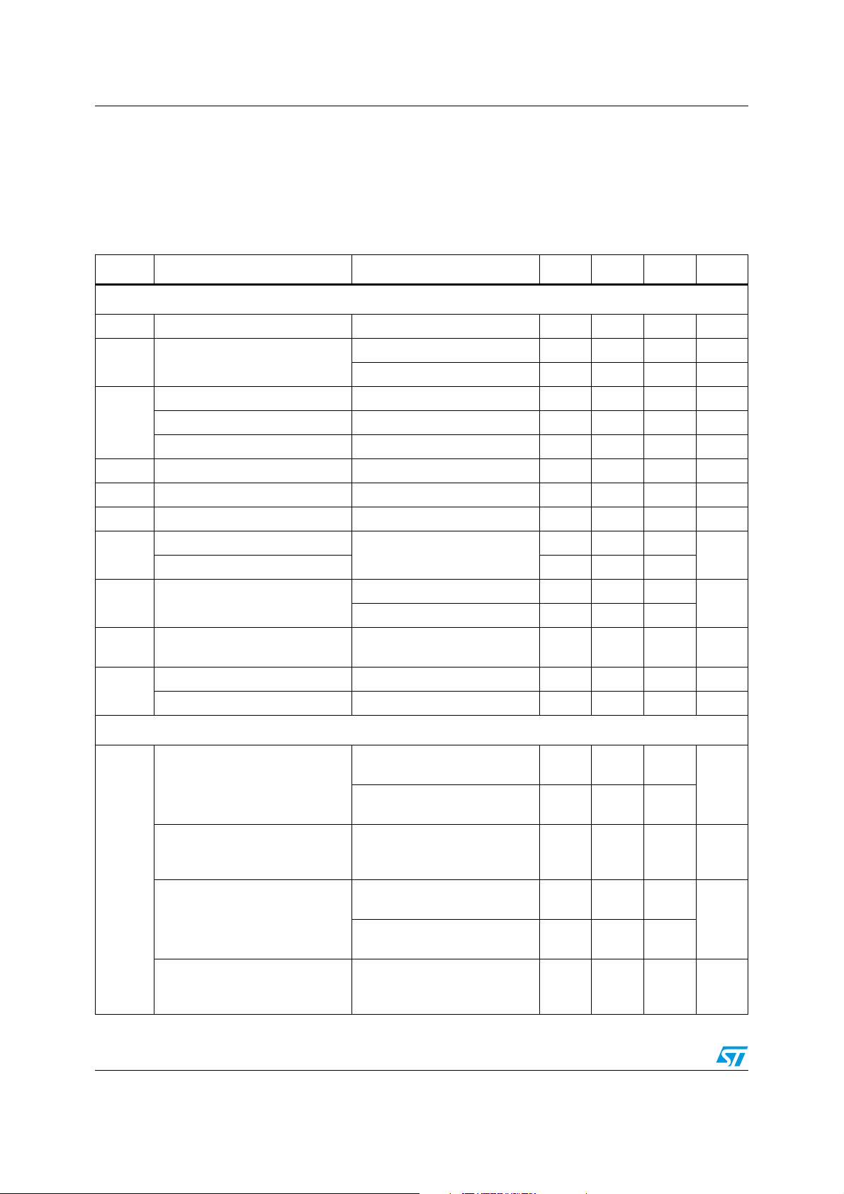
4 Electrical characteristics
- 40 °C < TA < 85 °C, CIN = 4.7 µF nominal, C
values are at T
Table 7. Electrical characteristics
= 25 °C, V
A
= VIN unless otherwise specified.
EN
= 4.7 µF nominal, L = 470 nH, typical
OUT
Symbol Parameter Test conditions Min. Typ. Max. Unit
General section
V
V
UVLO
Operating input voltage range 2.3 5.5 V
IN
V
rising 2.1 2.2 V
Undervoltage lockout threshold
IN
V
falling 1.8 1.9
IN
PFM mode quiescent current No load 45 60 µA
I
PWM mode quiescent current No load 15 mA
Q
f
SW
I
OUT
I
SC
I
PFM-
PWM
η
t
ON
Shutdown current V
Switching frequency 5.4 6 6.6 MHz
Continuous output current
Short-circuit current
(1)
(2)
PFM to PWM transition
PWM to PFM transition 100
Efficiency (V
= 3.6 V, V
IN
OUT
=
1.82 V)
Startup time
= 0 0.5 5 µA
EN
VIN ≥ V
+ 0.40 V 500 mA
OUT
1200 mA
200
= 3.6V, V
V
IN
I
= 10 mA PFM mode 80
OUT
I
= 150 mA 83
OUT
from low to high, V
V
EN
OUT
= 1.82 V
V, V
OUT
= 1.82 V
IN
= 3.6
260 µs
Thermal shutdown 125 °C
T
SHDN
Hysteresis 30 °C
mA
%
Output voltage
V
Accuracy (ST1S15x18R)
Load regulation
OUT
Accuracy (ST1S15x28R)
Load regulation
2.3 ≤ VIN ≤ 5.5 V, I
PWM mode, -40 ≤ T
2.3 ≤ V
≤ 5.5 V, I
IN
PFM mode, -40 ≤ T
2.3 ≤ VIN ≤ 5.5 V, V
= 0 to 500 mA, PWM
I
OUT
mode, -40 ≤ T
3.2 ≤ VIN ≤ 5.5 V, I
PWM mode, -40 ≤ T
3.2 ≤ V
≤ 5.5 V, I
IN
PFM mode, -40 ≤ T
3.2 ≤ V
I
OUT
≤ 5.5 V, V
IN
= 0 to 500 mA, PWM
mode, - 40 ≤ T
OUT
OUT
≤ 85 °C
A
OUT
OUT
≤ 85 °C
A
A
A
OUT
A
A
OUT
6/27 Doc ID 023280 Rev 1
= 10 mA,
≤ 85 °C
= 10 mA,
≤ 85 °C
=1.82 V,
= 10 mA,
≤ 85 °C
= 10 mA,
≤ 85 °C
= 2.8 V,
1.78 1.82 1.86
V
1.78 1.82 1.86
-1.5 %
2.74 2.8 2.86
V
2.74 2.8 2.86
-1.5 %

ST1S15 Electrical characteristics
Table 7. Electrical characteristics (continued)
Symbol Parameter Test conditions Min. Typ. Max. Unit
V
OUT_Rip
I
LKFB
Peak-to-Peak output voltage
ripple
ple
FB pin leakage current V
Line transient response.
Output voltage variation over
V
IN_TR
nominal DC level.
t
R
Case 1: V
Case 2: V
Load transient response
t
R=tF
I
OUT_TR
Case 1: V
Case 2: V
Case 3: V
Logic Inputs
V
V
Low-level input voltage (EN,
IL
MODE pins)
High-level input voltage (EN,
IH
MODE pins)
= tF = 10 µs
IN
IN
=0.1µs.
=2.5 V
IN
=3.6 V
IN
=4.5 V
IN
= 2.5 to 3.1 V
= 3.9 to 4.5 V
PWM mode, I
= 3.6 V, V
V
IN
PFM mode, I
= 3.6 V, V
V
IN
= 5.5 V 9 µA
FB
I
= 50 mA, V
OUT
OUT
OUT
= 150 mA,
OUT
OUT
OUT
= 150 mA,
= 1.82 V
= 1.82 V
= 1.82 V
10 mV
30 mV
±50 mV
I
= 250 mA, V
OUT
= 0 to 150 mA,
I
OUT
= 1.82 V
V
OUT
= 50 to 250 mA,
I
OUT
V
= 1.82 V
OUT
= 150 to 400 mA,
I
OUT
= 1.82 V
V
OUT
OUT
= 1.82 V
±50
±70
±70
0.4 V
1.2 V
mV
I
Input leakage current (EN, MODE
LK-I
pins)
= V
V
EN
= 5.5 V 0.01 1 µA
MODE
Power Switches
P-channel MOSFET onresistance
R
DSON
N-channel MOSFET onresistance
I
LPEAK
I
LKG-P
I
LKG-N
1. Not tested in production. This value is guaranteed by correlation with R
2. Not tested in production. This parameter is guaranteed by peak current limit.
P-channel peak current limit Over input voltage range 900 1000 1200 mA
P-channel leakage current V
N-channel leakage current V
= 5.5 V, VEN= 0 1 µA
IN
= 5.5 V, VEN= 0 1 µA
SW
DSON
300 400
mΩ
350 450
, peak current limit and operating input voltage.
Doc ID 023280 Rev 1 7/27

Typical performance characteristics ST1S15
5 Typical performance characteristics
Figure 3. Efficiency vs. output current
100
90
80
70
60
50
40
30
Efficiency [%]
20
10
0
1 10 100 1000
VEN = VIN, I
(V
= 1.82 V)
OUT
= 1 mA to 500 mA
OUT
Figure 4. Efficiency vs. output current
(V
= 2.8 V)
100
90
80
Vin= 2.5V PWM Mode
Vin= 2.5V PFM Mode
Vin= 3.6V PWM Mode
Vin= 3.6V PFM Mode
Vin= 4.5V PWM Mode
Vin= 4.5V PFM Mode
Vin= 5.5V PWM Mode
Vin= 5.5V PFM Mode
I
[mA]
OUT
70
60
50
40
30
Efficiency [%]
20
10
0
1 10 100 1000
VEN = VIN, I
OUT
= 1 mA to 500 mA
OUT
Vin= 3.2V PWM Mode
Vin= 3.2V PFM Mode
Vin= 3.6V PWM Mode
Vin= 3.6V PFM Mode
Vin= 4.2V PWM Mode
Vin= 4.2V PFM Mode
Vin= 5.0V PWM Mode
Vin= 5.0V PFM Mode
I
[mA]
OUT
Figure 5. Output voltage vs. input voltage Figure 6. Supply current vs. input voltage in
2.00
1.80
1.60
1.40
1.20
1.00
0.80
0.60
0.40
Output Voltage [V]
0.20
0.00
0 0.5 1 1.5 2 2.5 3 3.5 4 4.5 5 5.5 6
T=85°C
T=55°C
T=25°C
T=0°C
T= -25°C
T= -40°C
Input Voltage [V]
65
60
55
50
ISupply [µA]
45
40
35
2 2.5 3 3.5 4 4.5 5 5.5 6
auto mode
T= 85°C
T= 25°C
T= 0°C
T= -40° C
Input Voltage [V]
VIN = 0 to 5.5 V (step 0.1 V), I
= V
V
EN
IN
= 500 mA, Mode = GND,
OUT
Figure 7. Supply current vs. input voltage in
100
10
ISupply [mA]
1
2 2.5 3 3.5 4 4.5 5 5.5 6
VIN = 2.3 V to 5.5 V, Mode = VIN, V
PWM mode
Input Voltage [V]
= 1.82 V, VEN = V
OUT
T= 85°C
T= 25°C
T= 0°C
T= -40 °C
VIN = 2.5 V to 5.5 V, Mode = GND, V
Figure 8. Output voltage vs. output current
1.85
1.84
1.83
1.82
1.81
Output Voltage [V]
1.8
1.79
0 50 100 150 200 250 300 350 400 450 500 550
VEN = VIN, Mode = VIN, V
IN
8/27 Doc ID 023280 Rev 1
Output Current [mA ]
= 1.82 V
OUT
= 1.82 V, VEN = V
OUT
IN
Vin = 2.5 V
Vin = 3.6 V
Vin = 4.5 V

ST1S15 Typical performance characteristics
Figure 9. Frequency vs. input voltage Figure 10. Output voltage vs. output current
7.5
7
6.5
T= 85°C
T= 25°C
T= 0°C
T= - 40°C
6
5.5
Frequency [MHz]
5
4.5
22.5 33.5 44.5 55.5 6
Inp ut Voltage [V]
VIN = 2.3 V to 5.5 V, I
Figure 11. Mode transition vs. input voltage Figure 12. Mode transition PFM to PWM
250
200
150
100
Output Current [ mA ]
50
0
2 2.5 3 3.5 4 4.5 5 5.5 6
= 10 mA, Mode = V
OUT
IN, VEN
= V
PFM t o PWM
PWM to PFM
IN
1.89
1.87
1.85
1.83
1.81
1.79
Output Voltage [V]
1.77
1.75
0 50 100 150 200 250 300 350 400 450 500 550
Output Cur rent [ mA ]
VIN = 3.6 V, I
= 0 to 500 mA, Mode = GND, VEN = V
OUT
Mode
V
IN
V
OUT
I
L
Inpu t Voltage [V]
T= 85°C
T= 25°C
T= 0°C
T= - 40°C
IN
VIN = Enable, V
Figure 13. Mode transition PWM to PFM Figure 14. Output voltage ripple
= 1.82 V, Mode = GND
OUT
VIN = 3.6 V, V
= 1.82 V, Mode = 0 to 3.6 V, Load = 180 Ω
OUT
Mode
V
IN
V
OUT
I
L
VIN = 3.6 V, V
= 1.82 V, Mode = 3.6 to 0 V, Load = 180 Ω
OUT
VIN = 3.6 V, V
load
= 1.82 V, Mode = GND, VEN = V
OUT
Doc ID 023280 Rev 1 9/27
IN,
No

Typical performance characteristics ST1S15
Figure 15. Output voltage ripple Figure 16. Line transient
V
OUT
I
OUT
VIN = 3.6 V, V
Figure 17. Load transient I
,
V
OUT
I
OUT
VIN = 3.6 V, tr = 100 ns, I
Mode = GND
Figure 19. Enable startup Figure 20. VIN startup
= 1.82 V, I
OUT
= 500 mA, VEN = V
OUT
= 50 to 250 mA Figure 18. Load transient I
OUT
= 50 mA to 250 mA, VEN = V
OUT
IN
VIN = 3.9 to 4.5 V, tr = tf = 10 µs, I
V
OUT
I
OUT
VIN = 3.6 V, tf = 100 ns, I
IN,
Mode = GND
= 250 mA to 50 mA, VEN = V
OUT
EN
I
OUT
V
IN
= 50 mA, VEN = V
OUT
= 250 to 50 mA
OUT
IN
IN,
V
OUT
I
L
VIN = 3.6 V, Enable = 0 to 3.6 V, Mode = VIN, V
Load = 3.6 Ω
= 1.82 V,
OUT
V
IN
V
OUT
VIN = 0 to 2.5 V, Enable = VIN, Mode = GND, V
Load = 3.3 Ω
10/27 Doc ID 023280 Rev 1
= 1.82 V,
OUT

ST1S15 Block schematic
6 Block schematic
Figure 21. Block schematic
V-I Refer ence
EN
MODE
Enable & Soft Start
&
Prereg + UVLO
Cur rent Li mi t & Shor t Protec t.
V
IN
GND
PFM - Analog timing
Oscill.
&
Sawtooth
Swi tch Cont rol Log ic
PWM Comparator
PFM - PW M
Driver
&
Anti X- Cond
Ther mal Protec t.
Err or Amp & Comp.
Vref_PW M
SW
Vref_PF M
FB
R1
R2
AM11905v1
Doc ID 023280 Rev 1 11/27

Detailed description ST1S15
7 Detailed description
7.1 General description
The ST1S15 is a fixed voltage mode PWM step-down DC-DC converter which operates with
typically 6 MHz fixed frequency pulse width modulation (PWM) at moderate to heavy load
currents. At light load currents the converter can automatically enter PFM (pulse frequency
mode) mode.
To make the device work, few components are required: an inductor and two capacitors. It
has been designed to work properly with X5R or X7R SMD ceramic capacitors both at the
input and at the output. These kinds of capacitors, thanks to their very low series resistance
(ESR), minimize the output voltage ripple. In addition, the chosen inductor must be able to
not saturate at the peak current level.
7.2 Mode transition
The ST1S15 can work in PWM mode or in PFM mode according to the different operating
conditions. If the MODE pin is pulled high, the device works only in PWM mode even at light
or no load. If the MODE pin is low, the operation changes according to the average input
current handled by the device. At low output current the device works in PFM mode in order
to obtain very low power consumption and very good efficiency. When the output current
increases, the device automatically switches to PWM mode in order to deliver the power
needed by the load.
The ST1S15 passes from PFM to PWM when 3 consecutive PFM pulses occur. This means
that the PFM has reached its maximum current capability and the device needs to go into
PWM mode. The whole PWM circuitry starts after a transition time. During this time the
duration of the PFM pulses are increased to about 350 ns so as to provide higher current
capability. After startup of the PWM circuitry, the ST1S15 switches to PWM operation.
Figure 22. PFM to PWM transition
I
L
MODE
LOAD
I
PWM
PFM
500 mA
Consecutive 3 PFM pulses
t
Transition
Time
t
High Load
Light Load
AM11906v1
12/27 Doc ID 023280 Rev 1
t

ST1S15 Detailed description
The transition from PWM to PFM mode occurs when the load current decreases and the coil
current becomes negative. After the zero-crossing output goes up for 127 consecutive times
the device switches to PFM mode.
Figure 23. PWM to PFM transition
I
L
127 Zero-C rossing output pulses
t
PWM
MODE
PFM
t
LOAD
500 mA
I
High Load
AM11907v1
7.3 Soft-start
The internal soft-start is enabled after VIN reaches the UVLO threshold and the EN pin is
high or for startup after enable. An overtemperature shutdown event or over short-circuit
event also activates the soft-start sequence.
It eliminates the in-rush current problem during the startup phase. During the soft-start the
device works always in PWM regardless of the status of the Mode pin.
7.4 Short-circuit protection
The short-circuit protection begins when there is a short between the device output and
ground. In this case the output voltage value is lower than the voltage reference and the
overcurrent protection comparator output is high. When this happens the power stage (Pch
and Nch) turns off and a soft-start phase starts. The device repeats the soft-start sequence
during the short-circuit condition.
7.5 Undervoltage lockout (UVLO)
Light Load
t
The UVLO circuit prevents the device from malfunctioning when the input voltage is not high
enough. The device is in shutdown mode, when the input voltage is below the UVLO
threshold. The hysteresis of 200 mV prevents unstable operation when the input voltage is
close to the UVLO threshold.
Doc ID 023280 Rev 1 13/27

Detailed description ST1S15
7.6 Thermal protection
The device also has thermal shutdown protection, which is active when the junction
temperature reaches 125 °C. In this case both the high and low-side MOSFETs are turned
off.
Once the junction temperature goes back below 95 °C, the device resumes normal
operation.
7.7 Overcurrent protection
The overcurrent protection is used to limit the maximum inductor current. This current
flowing through the Pch of the power stage causes a voltage drop, across its RDSON, at the
switching node. A comparator compares the switching node voltage with a reference voltage
VR. To generate the VR voltage a current generator is used, which causes a drop across a
Pch of the same kind as the power stage. When the switching node voltage is lower than
VR, the comparator output goes high and the power Pch turns off.
7.8 Enable function
The ST1S15 features an enable function (pin 2 or B2). When the EN voltage is higher than
1.2 V the device is ON, and if it is lower than 0.4 V the device is OFF. In shutdown mode the
consumption is lower than 5 µA.
The EN pin does not have an internal pull-up, which means that the EN pin cannot be left
floating.
If the enable function is not used, the EN pin must be connected to V
IN
.
14/27 Doc ID 023280 Rev 1

ST1S15 Application Information
8 Application Information
8.1 Input and output capacitor
It is recommended to use ceramic capacitors with X5R or X7R dielectric and low ESR. The
input capacitor is used to filter any disturbance present in the input line and to obtain stable
operation. The output capacitor is very important to satisfy the output voltage ripple
requirement.
The output voltage ripple (V
Equation 1
where ΔI
is the ripple current and fSW is the switching frequency.
L
The use of ceramic capacitors with voltage ratings in the range higher than 1.5 times the
maximum input or output voltage is recommended.
8.2 Inductor
The inductor is the key passive component for switching converters. The internal
compensation is optimized to operate with an output filter of L = 0.47 µH and C
In addition to the inductance value, in order to avoid saturation, the maximum saturation
current of the inductor must be higher than that of the I
The peak current of the inductor must be calculated as:
Equation 2
OUT_RIPPLE
), in continuous mode, must be calculated:
⎡
+×Δ=
ESRIV
⎢
LRIP PLE_OUT
⎣
1
××
fC8
SWOUT
PEAK
⎤
×
ESLV
IN
+
⎥
L
⎦
.
= 4.7 µF.
OUT
)VV(V
II
+=
OU TPEAK
−×
OUTMAX_INOUT
LfV2
×××
SWMAX_IN
The following inductor p/ns from different suppliers have been tested in the ST1S15
converters.
Table 8. Inductors
Manufacturers p/ns Dimensions (in mm)
LQM21PNR47MC0D 2.0 x 1.25 x 0.5
Murata
TDK
Doc ID 023280 Rev 1 15/27
LQM21PNR54MG0D 2.0 x 1.25 x 0.5
LQH32PNR47NN0L 3.2 x 2.7 x 1.55
MLP2012SR47T 2.0 x 1.25 x 0.5
VLS2010ET-1R0N 2.0 x 2.0 x 1.0

Application Information ST1S15
8.3 Layout guidelines
Due to the high switching frequency and peak current, the layout is an important design step
for all switching power supplies. If the layout is not done carefully, important parameters
such as stability, efficiency, line and load regulation and output voltage ripple may be
compromised.
Short, wide traces must be implemented for main current and for power ground paths. The
input capacitor must be placed as close as possible to the device pin as well as the inductor
and output capacitor.
The FEEDBACK pin (FB) is a high impedance node, so the interference can be minimized
by placing the routing of the feedback node as far as possible from the high current paths.
A common ground node minimizes ground noise.
The exposed pad of the DFN package must be connected to the common ground node.
Figure 24. DFN layout recommended (not to scale)
V
OUT
C
OUT
GND
L
EN
AM11908v1
C
MODE
IN
V
IN
Figure 25. Flip-Chip layout recommended (not to scale)
V
OUT
C
OUT
L
AM11910v1
EN
GND
C
IN
V
IN
MODE
EN
16/27 Doc ID 023280 Rev 1

ST1S15 Package mechanical data
9 Package mechanical data
In order to meet environmental requirements, ST offers these devices in different grades of
®
ECOPACK
specifications, grade definitions and product status are available at:
packages, depending on their level of environmental compliance. ECOPACK
www.st.com
. ECOPACK
is an ST trademark.
Table 9. DFN6 (2 x 2 mm) mechanical data
(mm)
Dim.
Min. Typ. Max.
A 0.51 0.55 0.60
A1 0 0.02 0.05
b 0.18 0.25 0.30
D2.00
D2 1.30 1.45 1.55
E2.00
E2 0.85 1.00 1.10
e0.50
L 0.15 0.25 0.35
Doc ID 023280 Rev 1 17/27

Package mechanical data ST1S15
Figure 26. DFN6 (2 x 2 mm) package dimensions
18/27 Doc ID 023280 Rev 1
8128232_B

ST1S15 Package mechanical data
Figure 27. DFN6 footprint recommended data (dimensions in mm)
8128232_B
Doc ID 023280 Rev 1 19/27

Package mechanical data ST1S15
Table 10. Flip Chip 6 mechanical data
(mm)
Dim.
Min. Typ. Max.
A 0.52 0.56 0.6
A1 0.17 0.20 0.23
A2 0.35 0.36 0.37
b 0.23 0.25 0.29
D 0.905 0.935 0.965
D1 0.4
e0.4
E 1.16 1.19 1.22
E1 0.8
f
D
f
E
ccc 0.075
0.272
0.200
20/27 Doc ID 023280 Rev 1

ST1S15 Package mechanical data
Figure 28. Flip Chip 6 package dimensions
7504896_R
Doc ID 023280 Rev 1 21/27

Package mechanical data ST1S15
Figure 29. Flip Chip 6 footprint recommended data (dimensions in mm)
7504896_R
22/27 Doc ID 023280 Rev 1

ST1S15 Package mechanical data
Tape & reel QFNxx/DFNxx (2x2 mm) mechanical data
mm. inch.
Dim.
Min. Typ. Max. Min. Typ. Max.
A1807.087
C12.8 13.2 0.504 0.519
D 20.2 0.795
N60 2.362
T14.40.567
Ao 2.1 2.2 2.3 0.083 0.0870.091
Bo 2.1 2.2 2.3 0.083 0.0870.091
Ko 0.65 0.75 0.85 0.026 0.0300.033
Po 4 0.157
P4 0.157
Doc ID 023280 Rev 1 23/27

Package mechanical data ST1S15
Tape & reel Flip-Chip 6 mechanical data
mm.
Dim.
Min. Typ. Max.
A 180
C12.8 13.2
D20.2
N60
T 14.4
Ao 1.01 1.06 1.11
Bo 1.26 1.311.36
Ko 0.61 0.66 0.71
Po 3.9 4.1
P 3.9 4.1
24/27 Doc ID 023280 Rev 1

ST1S15 Different output voltage versions of the ST1S15 available on request
10 Different output voltage versions of the ST1S15
available on request
Table 11. Options available on request
Order codes Output voltages (V)
ST1S15x08R 0.8
ST1S15x10R 1
ST1S15x11R 1.05
ST1S15x12R 1.2
ST1S15x13R 1.25
ST1S15x15R 1.5
ST1S15x17R 1.8
ST1S15x19R 1.85
ST1S15x20R 1.875
ST1S15x25R 2.5
ST1S15x30R 3
ST1S15x33R 3.3
Doc ID 023280 Rev 1 25/27

Revision history ST1S15
11 Revision history
Table 12. Document revision history
Date Revision Changes
07-Jun-2012 1 First release.
26/27 Doc ID 023280 Rev 1

ST1S15
Please Read Carefully:
Information in this document is provided solely in connection with ST products. STMicroelectronics NV and its subsidiaries (“ST”) reserve the
right to make changes, corrections, modifications or improvements, to this document, and the products and services described herein at any
time, without notice.
All ST products are sold pursuant to ST’s terms and conditions of sale.
Purchasers are solely responsible for the choice, selection and use of the ST products and services described herein, and ST assumes no
liability whatsoever relating to the choice, selection or use of the ST products and services described herein.
No license, express or implied, by estoppel or otherwise, to any intellectual property rights is granted under this document. If any part of this
document refers to any third party products or services it shall not be deemed a license grant by ST for the use of such third party products
or services, or any intellectual property contained therein or considered as a warranty covering the use in any manner whatsoever of such
third party products or services or any intellectual property contained therein.
UNLESS OTHERWISE SET FORTH IN ST’S TERMS AND CONDITIONS OF SALE ST DISCLAIMS ANY EXPRESS OR IMPLIED
WARRANTY WITH RESPECT TO THE USE AND/OR SALE OF ST PRODUCTS INCLUDING WITHOUT LIMITATION IMPLIED
WARRANTIES OF MERCHANTABILITY, FITNESS FOR A PARTICULAR PURPOSE (AND THEIR EQUIVALENTS UNDER THE LAWS
OF ANY JURISDICTION), OR INFRINGEMENT OF ANY PATENT, COPYRIGHT OR OTHER INTELLECTUAL PROPERTY RIGHT.
UNLESS EXPRESSLY APPROVED IN WRITING BY TWO AUTHORIZED ST REPRESENTATIVES, ST PRODUCTS ARE NOT
RECOMMENDED, AUTHORIZED OR WARRANTED FOR USE IN MILITARY, AIR CRAFT, SPACE, LIFE SAVING, OR LIFE SUSTAINING
APPLICATIONS, NOR IN PRODUCTS OR SYSTEMS WHERE FAILURE OR MALFUNCTION MAY RESULT IN PERSONAL INJURY,
DEATH, OR SEVERE PROPERTY OR ENVIRONMENTAL DAMAGE. ST PRODUCTS WHICH ARE NOT SPECIFIED AS "AUTOMOTIVE
GRADE" MAY ONLY BE USED IN AUTOMOTIVE APPLICATIONS AT USER’S OWN RISK.
Resale of ST products with provisions different from the statements and/or technical features set forth in this document shall immediately void
any warranty granted by ST for the ST product or service described herein and shall not create or extend in any manner whatsoever, any
liability of ST.
ST and the ST logo are trademarks or registered trademarks of ST in various countries.
Information in this document supersedes and replaces all information previously supplied.
The ST logo is a registered trademark of STMicroelectronics. All other names are the property of their respective owners.
© 2012 STMicroelectronics - All rights reserved
STMicroelectronics group of companies
Australia - Belgium - Brazil - Canada - China - Czech Republic - Finland - France - Germany - Hong Kong - India - Israel - Italy - Japan -
Malaysia - Malta - Morocco - Philippines - Singapore - Spain - Sweden - Switzerland - United Kingdom - United States of America
www.st.com
Doc ID 023280 Rev 1 27/27
 Loading...