


2 A, 1.5 MHz PWM step-down switching regulator
Features
■ 1.5 MHz fixed frequency PWM with current
control mode
■ 2 A output current capability
■ Typical efficiency: > 90%
■ 2 % DC output voltage tolerance
■ Two versions available: power good or inhibit
■ Integrated output over-voltage protection
■ Non switching quiescent current: (typ) 1.5 mA
over temperature range
■ R
■ Utilizes tiny capacitors and inductors
■ Operating junction temp. -30 °C to 125 °C
■ Available in DFN6 (3 x 3 mm) exposed pad
Description
The ST1S09 is a step-down DC-DC converter
optimized for powering low output voltage
applications. It supplies a current in excess of 2 A
over an input voltage range from 2.7 V to 6 V.
A high PWM switching frequency (1.5 MHz)
allows the use of tiny surface-mount components.
(typ) 100 mΩ
DSON
ST1S09
with synchronous rectification
DFN6 (3 x 3 mm)
Moreover, since the required synchronous
rectifier is integrated, the number of the external
components is reduced to minimum: a resistor
divider, an inductor and two capacitors. The
Power Good function continuously monitors the
output voltage. An open drain Power Good flag is
released when the output voltage is within
regulation. In addition, a low output ripple is
guaranteed by the current mode PWM topology
and by the use of low ESR SMD ceramic
capacitors. The device is thermally protected and
the output current limited to prevent damages due
to accidental short circuit. The ST1S09 is
available in the DFN6 (3 x 3 mm) package.
Table 1. Device summary
Order codes Package
ST1S09PUR DFN6D (3 x 3 mm)
ST1S09APUR
ST1S09IPUR DFN6D (3 x 3 mm)
1. Available on request.
April 2010 Doc ID 13632 Rev 4 1/18
(1)
DFN6D (3 x 3 mm)
www.st.com
18

ST1S09
Contents
1 Diagram . . . . . . . . . . . . . . . . . . . . . . . . . . . . . . . . . . . . . . . . . . . . . . . . . . . 3
2 Pin configuration . . . . . . . . . . . . . . . . . . . . . . . . . . . . . . . . . . . . . . . . . . . . 4
3 Maximum ratings . . . . . . . . . . . . . . . . . . . . . . . . . . . . . . . . . . . . . . . . . . . . 5
4 Electrical characteristics . . . . . . . . . . . . . . . . . . . . . . . . . . . . . . . . . . . . . 6
5 Typical performance characteristics . . . . . . . . . . . . . . . . . . . . . . . . . . . . 8
6 Typical application . . . . . . . . . . . . . . . . . . . . . . . . . . . . . . . . . . . . . . . . . 11
7 Application information . . . . . . . . . . . . . . . . . . . . . . . . . . . . . . . . . . . . . 12
8 Package mechanical data . . . . . . . . . . . . . . . . . . . . . . . . . . . . . . . . . . . . 13
9 Revision history . . . . . . . . . . . . . . . . . . . . . . . . . . . . . . . . . . . . . . . . . . . 17
2/18 Doc ID 13632 Rev 4
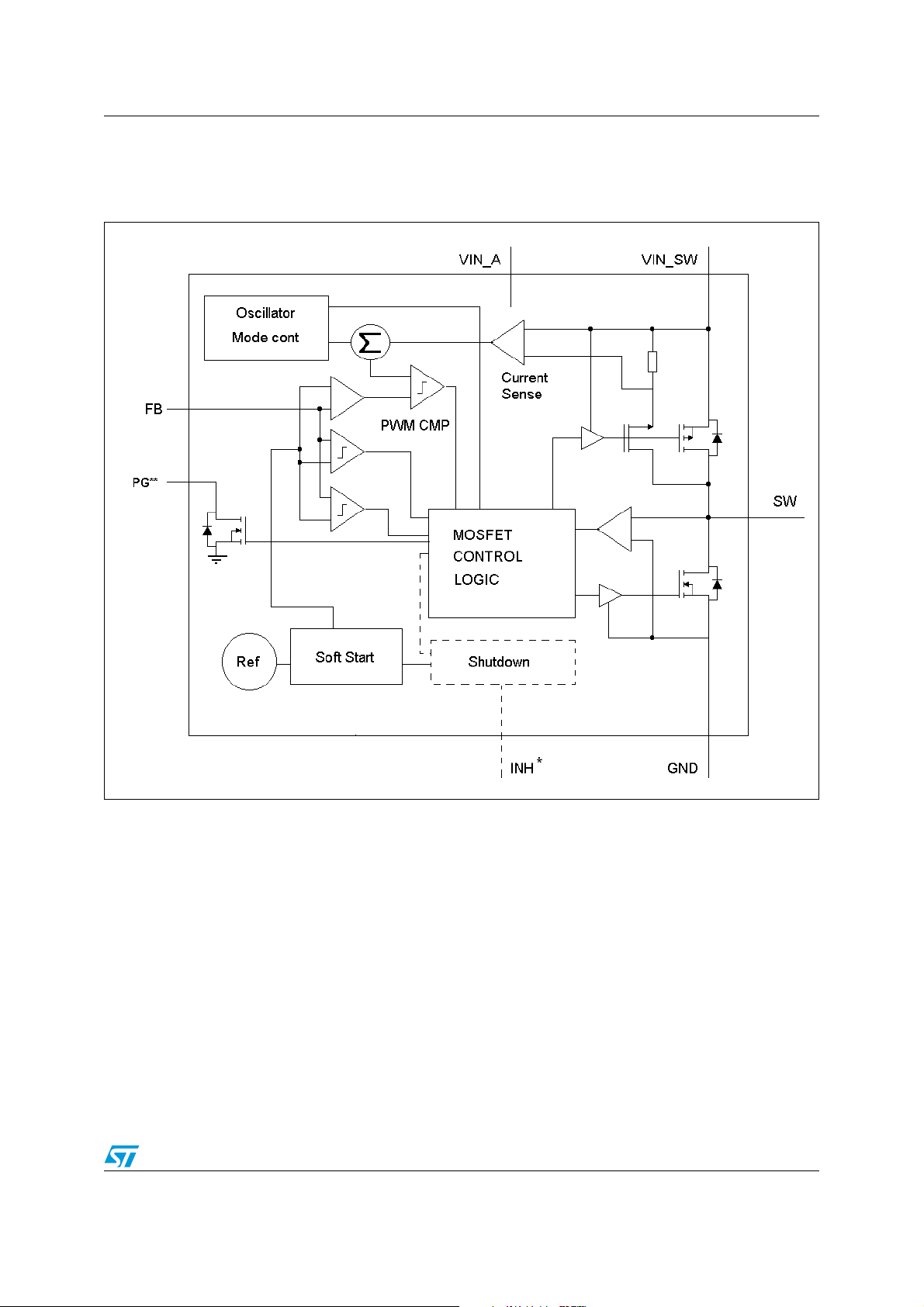
ST1S09 Diagram
1 Diagram
Figure 1. Schematic diagram
(*) Only for ST1S09IPU
(**) Only for ST1S09PU
Doc ID 13632 Rev 4 3/18
Pin configuration ST1S09
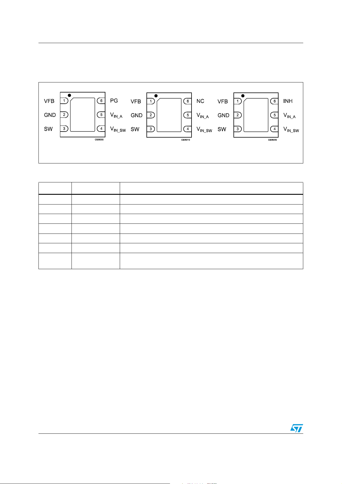
2 Pin configuration
Figure 2. Pin connections (top view)
ST1S09
ST1S09A
Table 2. Pin description
Pin n° Symbol Name and function
1 FB Feedback voltage
2 GND System ground
3 SW Switching pin
4V
5V
6 INH/PG/NC Inhibit (to turn off the device) / Power Good / Not Connected
Exposed
Pad
IN_SW
IN_A
GND
Power supply for the MOSFET switch
Power supply for analog circuit
To be connected to PCB ground plane for optimal electrical and thermal
performance
ST1S09I
4/18 Doc ID 13632 Rev 4
ST1S09 Maximum ratings
3 Maximum ratings
Table 3. Absolute maximum ratings
Symbol Parameter Value Unit
V
IN_SW
V
V
IN_A
INH
Positive power supply voltage -0.3 to 7 V
Positive power supply voltage -0.3 to 7 V
Inhibit voltage (I version) -0.3 to VI + 0.3 V
SWITCH Voltage Max. voltage of output pin -0.3 to 7 V
V
FB
Feedback voltage -0.3 to 3 V
PG Power Good open drain -0.3 to 7 V
T
T
T
J
STG
LEAD
Max junction temperature -40 to 150 °C
Storage temperature range -65 to 150 °C
Lead temperature (soldering) 10 sec 260 °C
Note: Absolute maximum ratings are those values beyond which damage to the device may occur.
Functional operation under these conditions is not implied.
Table 4. Thermal data
Symbol Parameter Value Unit
R
thJC
R
thJA
Thermal resistance junction-case 10 °C/W
Thermal resistance junction-ambient 55 °C/W
Table 5. ESD performance
Symbol Parameter Test conditions Value Unit
ESD ESD protection voltage HBM 2 kV
ESD ESD protection voltage MM 500 V
Doc ID 13632 Rev 4 5/18
Electrical characteristics ST1S09
4 Electrical characteristics
Refer to Figure 21 application circuit V
C
= 22 µF, L1 = 2.7 µH, TJ = -30 to 125 °C (unless otherwise specified. Typical values are
2
IN_SW
= V
= 5 V, VO = 1.2 V, C1 = 4.7 µF,
IN_A
referred to 25 °C)
Table 6. Electrical characteristics for ST1S09PU
Symbol Parameter Test conditions Min. Typ. Max. Unit
FB Feedback voltage 784 800 816 mV
I
FB
V
UV
LO
OVP
I
OVP
I
Q
I
O
%VO/ΔVIOutput line regulation VI = 4.5 V to 5.5 V, IO = 100 mA
%VO/ΔIOOutput load regulation IO = 10 mA to 2 A
PWMf
D
MAX
PG
R
DSON
R
DSON
I
SWL
ν
T
SHDN
T
HYS
%VO/ΔIOLoad transient response
VFB pin bias current 600 nA
Input voltage IO = 10 mA to 2 A 4.5 5.5 V
I
Rising 3.5 3.7 3.9 V
V
Under voltage lock out
threshold
Over voltage protection
threshold
Over voltage protection
hysteresis
I
Hysteresis 150 mV
V
rising 1.05 VO1.1 V
O
falling 5 %
V
O
O
Overvoltage clamping current VO = 1.2 V 300 mA
Quiescent current Not switching 1.5 2.5 mA
Output current VI = 4.5 to 5.5 V
PWM switching frequency VFB = 0.65 V 1.2 1.5 1.8 MHz
S
(1)
(1)
2A
(1)
0.16
0.2 0.6 %
Maximum duty cycle 80 87 %
Power good output threshold 0.92 V
Power good output voltage low I
= 6 mA open drain output 0.4 V
SINK
O
-N NMOS switch on resistance ISW = 750 mA 0.1 Ω
-P PMOS switch on resistance ISW = 750 mA 0.1 Ω
Switching current limitation
Efficiency
(1)
(1)
2.5 2.9 3.5 A
IO = 10 mA to 100 mA, VO = 3.3 V 65
= 100 mA to 2 A, VO = 3.3 V 82 87
I
O
Thermal shutdown 150 °C
Thermal shutdown hysteresis 20 °C
= 100 mA to 1 A, TA = 25 °C
I
O
tR = tF ≥ 200 ns
(1)
-10 +10 %V
%V
ΔV
%
V
/
O
I
V
O
I
= 10 mA to IO = short,
%VO/ΔIOShort circuit removal response
1. Guaranteed by design, but not tested in production.
O
TA = 25 °C
(1)
6/18 Doc ID 13632 Rev 4
-10 +10 %V
O

ST1S09 Electrical characteristics
Refer to Figure 22 application circuit V
C2 = 22 µF, L1 = 2.7 µH, T
= -30 to 125 °C (unless otherwise specified. Typical values are
J
IN_SW
= V
IN_A
= V
= 5 V, VO = 1.2 V, C1 = 4.7 µF,
INH
referred to 25 °C)
Table 7. Electrical characteristics for ST1S09IPU
Symbol Parameter Test conditions Min. Typ. Max. Unit
FB Feedback voltage 784 800 816 mV
I
FB
V
OVP
I
Q
I
O
V
INH
I
INH
%VO/ΔVIOutput line regulation VI = 2.7 V to 5.5 V, IO = 100 mA
%VO/ΔIOOutput load regulation IO = 10 mA to 2 A
PWMfSPWM switching frequency VFB = 0.65 V 1.2 1.5 1.8 MHz
D
MAX
R
DSON
R
DSON
I
SWL
ν
T
SHDN
T
HYS
%VO/ΔIOLoad transient response
%VO/ΔIOShort circuit removal response
1. Guaranteed by design, but not tested in production.
VFB pin bias current 600 nA
Minimum input voltage IO = 10 mA to 2 A 2.7 V
I
Over voltage protection
threshold
Over voltage protection
hysteresis
Quiescent current
Output current VI = 2.7 to 5.5 V
Inhibit threshold
VO rising 1.05 VO1.1 V
V
falling 5 %
O
V
> 1.2 V, not switching 1.5 2.5 mA
INH
< 0.4 V, T = - 30 °C to 85 °C 1 µA
V
INH
Device ON, V
(1)
= 2.7 to 5.5 V 1.3
I
= 2.7 to 5 V 1.2
I
2A
O
Device OFF 0.4
Inhibit pin current 2µA
(1)
(1)
0.16
0.2 0.6
Maximum duty cycle 80 87 %
-N NMOS switch on resistance ISW = 750 mA 0.1 Ω
-P PMOS switch on resistance ISW = 750 mA 0.1 Ω
Switching current limitation
Efficiency
(1)
(1)
2.5 2.9 3.5 A
IO = 10 mA to 100 mA, VO = 3.3 V 65
= 100 mA to 2 A, VO = 3.3 V 82 87
I
O
Thermal shutdown 150 °C
Thermal shutdown hysteresis 20 °C
I
= 100 mA to 1 A, TA = 25 °C
O
tR = tF ≥ 200 ns
= 10 mA to IO = short,
I
O
= 25 °C
T
A
(1)
(1)
-10 +10 %V
-10 +10 %V
%V
ΔV
%V
ΔI
%
V
VDevice ON, V
/
O
I
/
O
O
O
O
Doc ID 13632 Rev 4 7/18

Typical performance characteristics ST1S09
5 Typical performance characteristics
L = 3.3 µH, CI = 4.7 µF, CO = 22 µF, unless otherwise specified.
Figure 3. Voltage feedback vs. temperature Figure 4. Feedback pin bias current vs. temp.
840
840
830
830
820
820
810
810
[mV]
[mV]
800
800
FBK
FBK
790
790
V
V
780
780
770
770
760
760
=5V, IO=10mA
=5V, IO=10mA
V
V
I
I
-75 -50 -25 0 25 50 75 100 125 150 175
-75 -50 -25 0 25 50 75 100 125 150 175
T [°C]
T [°C]
VO@1.2V
VO@1.2V
840
840
740
740
640
640
540
540
[nA]
[nA]
440
440
340
340
FBK
FBK
I
I
240
240
140
140
40
40
-60
-60
-75 -50 -25 0 25 50 75 100 125 150 175
-75 -50 -25 0 25 50 75 100 125 150 175
T [°C]
T [°C]
VI=5V
VI=5V
Figure 5. Quiescent current non switching
3
3
2.5
2.5
2
2
1.5
1.5
Iq [mA]
Iq [mA]
1
1
0.5
0.5
0
0
-75 -50 -25 0 25 50 75 100 125 150 175
-75 -50 -25 0 25 50 75 100 125 150 175
Figure 7. Inhibit voltage vs. input voltage Figure 8. Output voltage vs. input voltage
1.6
1.6
1.4
1.4
1.2
1.2
1
1
[V]
[V]
0.8
0.8
INH
INH
V
V
0.6
0.6
0.4
0.4
0.2
0.2
0
0
vs. temperature
VI=5V VO@1.2V
VI=5V
T [°C]
T [°C]
VI=from 2.7 to 5.5V, IO=2A
VI=from 2.7 to 5.5V, IO=2A
234567
234567
[V]
[V]
V
V
I
I
VO@1.2V
ON OFF
ON OFF
Figure 6. Inhibit voltage vs. temperature
1.6
1.6
1.4
1.4
1.2
1.2
1
1
[V]
[V]
0.8
0.8
INH
INH
V
V
0.6
0.6
0.4
0.4
0.2
0.2
VI=5V, IO=from 10mA to 2A
VI=5V, IO=from 10mA to 2A
0
0
-75 -50 -25 0 25 50 75 100 125 150 175
-75 -50 -25 0 25 50 75 100 125 150 175
T [°C]
T [°C]
1.40
1.40
V
V
@1.2V
@1.2V
O
O
V
V
CC =VINH
CC =VINH
0123456
0123456
VI[V]
VI[V]
[V]
[V]
O
O
V
V
1.20
1.20
1.00
1.00
0.80
0.80
0.60
0.60
0.40
0.40
0.20
0.20
0.00
0.00
ON OFF
ON OFF
=from 0 to 5.5V, IO=2A
=from 0 to 5.5V, IO=2A
8/18 Doc ID 13632 Rev 4

ST1S09 Typical performance characteristics
Figure 9. Line regulation vs. temperature Figure 10. Load regulation vs. temperature
1.1
]
]
/ΔI
/ΔI
load [%V
load [%V
O
O
O
O
1.1
0.9
0.9
0.7
0.7
0.5
0.5
0.3
0.3
0.1
0.1
-0.1
-0.1
-0.3
-0.3
-0.5
-0.5
VO@1.2V
VO@1.2V
-75 -50 -25 0 25 50 75 100 125 150 175
-75 -50 -25 0 25 50 75 100 125 150 175
= 5V, IOfrom10mA to 2A
= 5V, IOfrom10mA to 2A
V
V
I
I
T [°C]
T [°C]
1
1
0.8
0.8
VO@1.2V VI = from 2.7V to 5.5V, IO = 100mA
VO@1.2V VI = from 2.7V to 5.5V, IO = 100mA
0.6
0.6
]
]
I
I
0.4
0.4
t/ΔV
t/ΔV
0.2
0.2
O
O
0
0
-0.2
-0.2
-0.4
-0.4
line [%V
line [%V
-0.6
-0.6
-0.8
-0.8
-1
-1
-75 -50 -25 0 25 50 75 100 125 150 175
-75 -50 -25 0 25 50 75 100 125 150 175
T [°C]
T [°C]
Figure 11. PWM Switching frequency vs.
2
2
1.9
1.9
1.8
1.8
1.7
1.7
1.6
1.6
1.5
1.5
1.4
1.4
1.3
1.3
PWM freq.[MHz]
PWM freq.[MHz]
1.2
1.2
1.1
1.1
1
1
-75 -50 -25 0
-75 -50 -25 0
temperature
25
25
VI=5V, VFB=0.6VVO@1.2V
VI=5V, VFB=0.6VVO@1.2V
50 75 100 125 150 175
50 75 100 125 150 175
T [°C]
T [°C]
Figure 13. Under voltage lock out threshold
4
4
3.9
3.9
3.8
3.8
3.7
3.7
3.6
3.6
3.5
3.5
3.4
3.4
UVLO [V]
UVLO [V]
3.3
3.3
3.2
3.2
3.1
3.1
3
3
vs. temperature
V
VO@1.2V
@1.2V
O
-75 -50 -25 0 25 50 75 100 125 150 175
-75 -50 -25 0 25 50 75 100 125 150 175
T [°C]
T [°C]
IO=10mA
IO=10mA
Figure 12. Maximum duty cycle vs.
temperature
90
90
88
88
86
86
84
84
82
82
80
80
78
78
Dmax[%]
Dmax[%]
76
76
74
74
VO@3.3V
72
72
70
70
-75 -50 -25 0 25 50 75 100 125 150 175
-75 -50 -25 0 25 50 75 100 125 150 175
T [°C]
T [°C]
VI=5V, VFB=0.6VVO@3.3V
VI=5V, VFB=0.6V
Figure 14. Efficiency vs. output current
95
85
75
65
55
Efficiency [%]
45
35
25
0 500 1000 1500 2000
V
=1.2V
O
VIN=5V
Iout [mA]
VO=3.3V
Doc ID 13632 Rev 4 9/18
Typical performance characteristics ST1S09
Figure 15. Efficiency vs. temperature Figure 16. Over voltage protection vs.
100
100
95
95
90
90
85
85
80
80
75
75
70
70
65
65
60
60
Efficiency [%]
Efficiency [%]
55
55
50
50
45
45
40
40
-75 -50 -25 0 25 50 75 100 125 150 175
-75 -50 -25 0 25 50 75 100 125 150 175
VO=3.3V
VO=3.3V
VI=5V, IO=100mA
VI=5V, IO=100mA
T [°C]
T [°C]
VO=1.2V
VO=1.2V
1.4
1.4
1.3
1.3
1.2
1.2
O
O
1.1
1.1
1
1
OVP %V
OVP %V
0.9
0.9
0.8
0.8
-75 -50 -25 0 25 50 75 100 125 150 175
-75 -50 -25 0 25 50 75 100 125 150 175
temperature
Resistor 1.2kΩ from V
Resistor 1.2kΩ from V
VSW=1.2V
VSW=1.2V
OVP ON
OVP ON
and V
and V
I
SW
I
SW
VI=5V, VO=3.3V, CFB=100nF
VI=5V, VO=3.3V, CFB=100nF
T [°C]
T [°C]
Figure 17. Over voltage protection vs.
1.4
1.4
1.3
1.3
1.2
1.2
O
O
1.1
1.1
1
1
OVP %V
OVP %V
0.9
0.9
0.8
0.8
-75 -50 -25 0 25 50 75 100 125 150 175
-75 -50 -25 0 25 50 75 100 125 150 175
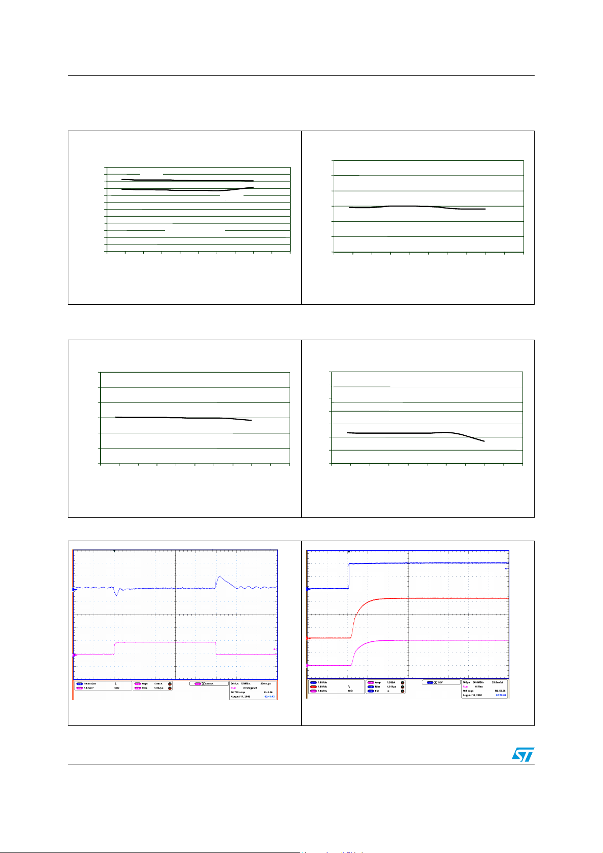
Figure 19. Load transient Figure 20. Inhibit transient
temperature
and V
OVP ON
OVP ON
and V
I
I
T [°C]
T [°C]
SW
SW
Resistor 1.2kΩ from V
Resistor 1.2kΩ from V
VSW=0.8V VI=5V, VO=3.3V, CFB=100nF
VSW=0.8V VI=5V, VO=3.3V, CFB=100nF
Figure 18. Over voltage protection hyst. vs.
temperature
14
14
Resistor 1.2kΩ from V
Resistor 1.2kΩ from V
12
12
VSW=0.8V VI=5V, VO=3.3V, CFB=100nF
VSW=0.8V VI=5V, VO=3.3V, CFB=100nF
10
10
8
8
6
6
4
4
OVP % Hysteresis
OVP % Hysteresis
2
2
0
0
-75 -50 -25 0 25 50 75 100 125 150 175
-75 -50 -25 0 25 50 75 100 125 150 175
V
V
O
O
and V
and V
I
I
OVP ON
OVP ON
T [°C]
T [°C]
SW
SW
V
V
INH
INH
I
I
O
O
VI = 5 V, VO = 1.2 V, IO = 100 mA to1 A, L = 3.3 µH,
C
= 4.7 µF, CO = 22 µF
I
VI = 5V, V
C
= 22 µF, VO = 3.3 V
O
10/18 Doc ID 13632 Rev 4
= 0 to 2 V, IO = 2 A, L = 3.3 µH, CI = 4.7 µF,
INH
V
V
O
O
I
I
O
O

ST1S09 Typical application
6 Typical application
Figure 21. Application circuits
Figure 22. Application circuits
Doc ID 13632 Rev 4 11/18

Application information ST1S09
7 Application information
The ST1S09 is an adjustable current mode PWM step-down DC-DC converter with internal
2 A power switch, packaged in a DFN6 3 x 3 mm.
The device is a complete 2 A switching regulator with its internal compensation eliminating
the need for additional components.
The constant frequency, current mode, PWM architecture and stable operation with ceramic
capacitors results in low, predictable output ripple.
The over-voltage protection circuit acts when the output voltage is over 10 % of the rated
voltage and within 200 ns the low side MOSFET will be turned on to clamp the output
transient. The current limit for clamping is about 400 mA. When the output voltage drops to
about 5 % above the nominal level, the device returns to nominal closed loop switching
operation.
The open drain Power Good (PG) pin is released when the output voltage is higher than
0.92 x V
Other circuits fitted to the device protection are the thermal shut-down block, which turns off
the regulator when the junction temperature exceeds 150 °C (typ), and the cycle-by-cycle
current limiting, which provides protection against shorted outputs.
. If the output voltage is below 0.92 x VO, the PG pin goes to low impedance.
O_NOM
As an adjustable regulator, the ST1S09’s output voltage is determined by an external
resistor divider. The desired value is given by the following equation:
Equation 1
V
= VFB [1 + R1 / R2]
O
To utilize the device, only a few components are required: an inductor, two capacitors and
the resistor divider. The inductor chosen must be able to reach peak current level without
saturating. Its value can be selected while taking into account that a large inductor value
increases the efficiency at low output current and reduces output voltage ripple, while a
smaller inductor can be chosen when it is important to reduce package size and the total
cost of the application. Finally, the ST1S09 has been designed to work properly with X5R or
X7R SMD ceramic capacitors both at the input and at the output. These types of capacitors,
due to their very low series resistance (ESR), minimize the output voltage ripple. Other low
ESR capacitors can be used according to the need of the application without compromising
the correct functioning of the device.
12/18 Doc ID 13632 Rev 4

ST1S09 Package mechanical data
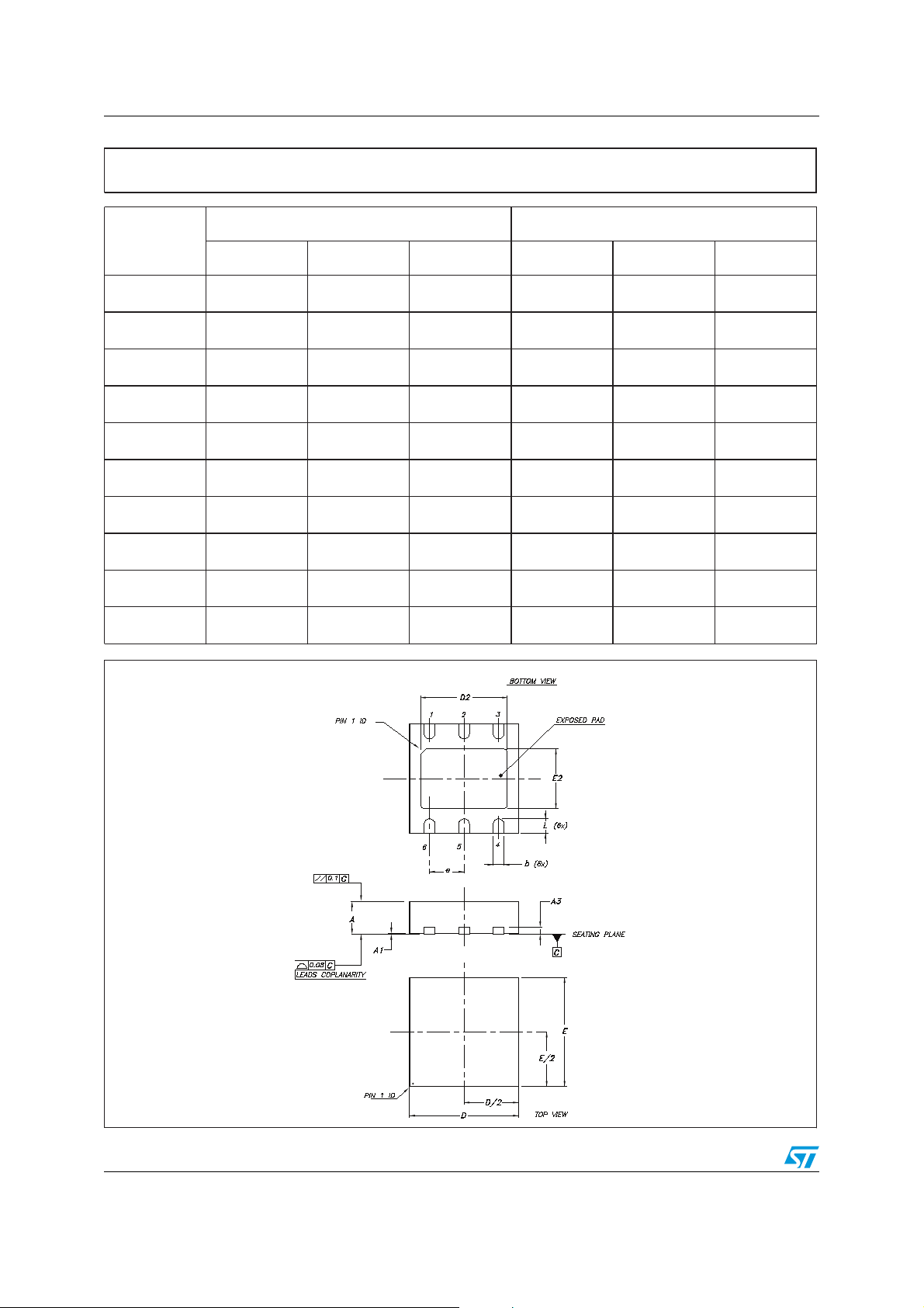
8 Package mechanical data
In order to meet environmental requirements, ST offers these devices in different grades of
ECOPACK
specifications, grade definitions and product status are available at: www.st.com.
ECOPACK
®
packages, depending on their level of environmental compliance. ECOPACK®
®
is an ST trademark.
Doc ID 13632 Rev 4 13/18
Package mechanical data ST1S09
DFN6D (3x3) Mechanical Data
mm. inch.
Dim.
Min. Typ. Max. Min. Typ. Max.
A0.801.000.0310.039
A1 0 0.02 0.05 0 0.001 0.002
A3 0.20 0.008
b 0.23 0.45 0.009 0.018
D2.90 3.00 3.10 0.114 0.118 0.122
D2 2.23 2.50 0.088 0.098
E2.90 3.00 3.10 0.114 0.118 0.122
E2 1.50 1.75 0.059 0.069
e0.950.037
L0.30 0.40 0.50 0.012 0.016 0.020
14/18 Doc ID 13632 Rev 4
7946637B

ST1S09 Package mechanical data
Figure 23. DFN6 (3 x 3 mm) footprint recommended data
Doc ID 13632 Rev 4 15/18

Package mechanical data ST1S09
Tape & Reel QFNxx/DFNxx (3x3) Mechanical Data
mm. inch.
Dim.
Min. Typ. Max. Min. Typ. Max.
A 330 12.992
C 12.8 13.2 0.504 0.519
D 20.2 0.795
N60 2.362
T18.4 0.724
Ao 3.3 0.130
Bo 3.3 0.130
Ko 1.1 0.043
Po 4 0.157
P 8 0.315
16/18 Doc ID 13632 Rev 4

ST1S09 Revision history
9 Revision history
Table 8. Document revision history
Date Revision Changes
18-Jun-2007 1 First release.
05-Jul-2007 2 Removed incorrect watermark.
31-Jan-2008 3 Modified: Table 6 on page 6.
19-Apr-2010 4 Modified: Table 1 on page 1.
Doc ID 13632 Rev 4 17/18

ST1S09
Please Read Carefully:
Information in this document is provided solely in connection with ST products. STMicroelectronics NV and its subsidiaries (“ST”) reserve the
right to make changes, corrections, modifications or improvements, to this document, and the products and services described herein at any
time, without notice.
All ST products are sold pursuant to ST’s terms and conditions of sale.
Purchasers are solely responsible for the choice, selection and use of the ST products and services described herein, and ST assumes no
liability whatsoever relating to the choice, selection or use of the ST products and services described herein.
No license, express or implied, by estoppel or otherwise, to any intellectual property rights is granted under this document. If any part of this
document refers to any third party products or services it shall not be deemed a license grant by ST for the use of such third party products
or services, or any intellectual property contained therein or considered as a warranty covering the use in any manner whatsoever of such
third party products or services or any intellectual property contained therein.
UNLESS OTHERWISE SET FORTH IN ST’S TERMS AND CONDITIONS OF SALE ST DISCLAIMS ANY EXPRESS OR IMPLIED
WARRANTY WITH RESPECT TO THE USE AND/OR SALE OF ST PRODUCTS INCLUDING WITHOUT LIMITATION IMPLIED
WARRANTIES OF MERCHANTABILITY, FITNESS FOR A PARTICULAR PURPOSE (AND THEIR EQUIVALENTS UNDER THE LAWS
OF ANY JURISDICTION), OR INFRINGEMENT OF ANY PATENT, COPYRIGHT OR OTHER INTELLECTUAL PROPERTY RIGHT.
UNLESS EXPRESSLY APPROVED IN WRITING BY AN AUTHORIZED ST REPRESENTATIVE, ST PRODUCTS ARE NOT
RECOMMENDED, AUTHORIZED OR WARRANTED FOR USE IN MILITARY, AIR CRAFT, SPACE, LIFE SAVING, OR LIFE SUSTAINING
APPLICATIONS, NOR IN PRODUCTS OR SYSTEMS WHERE FAILURE OR MALFUNCTION MAY RESULT IN PERSONAL INJURY,
DEATH, OR SEVERE PROPERTY OR ENVIRONMENTAL DAMAGE. ST PRODUCTS WHICH ARE NOT SPECIFIED AS "AUTOMOTIVE
GRADE" MAY ONLY BE USED IN AUTOMOTIVE APPLICATIONS AT USER’S OWN RISK.
Resale of ST products with provisions different from the statements and/or technical features set forth in this document shall immediately void
any warranty granted by ST for the ST product or service described herein and shall not create or extend in any manner whatsoever, any
liability of ST.
ST and the ST logo are trademarks or registered trademarks of ST in various countries.
Information in this document supersedes and replaces all information previously supplied.
The ST logo is a registered trademark of STMicroelectronics. All other names are the property of their respective owners.
© 2010 STMicroelectronics - All rights reserved
STMicroelectronics group of companies
Australia - Belgium - Brazil - Canada - China - Czech Republic - Finland - France - Germany - Hong Kong - India - Israel - Italy - Japan -
Malaysia - Malta - Morocco - Philippines - Singapore - Spain - Sweden - Switzerland - United Kingdom - United States of America
www.st.com
18/18 Doc ID 13632 Rev 4
 Loading...