

1.5 A, 1.5 MHz adjustable, with inhibit function
Features
■ Step-down current mode PWM (1.5 MHz) DC-
DC converter
■ 2 % DC output voltage tolerance
■ Internal soft start for start-up current limitation
and power on delay of 50-100 µs
■ Typical efficiency: > 85 %
■ Inhibit function
■ 1.5 A output current capability
■ Not switching quiescent current: max 1.5 mA
over temperature range
■ Switch V
■ Uses tiny capacitors and inductors
■ Available in DFN6D 3x3 exposed pad
: max 200 mV @ I
DS
= 750 mA
SW
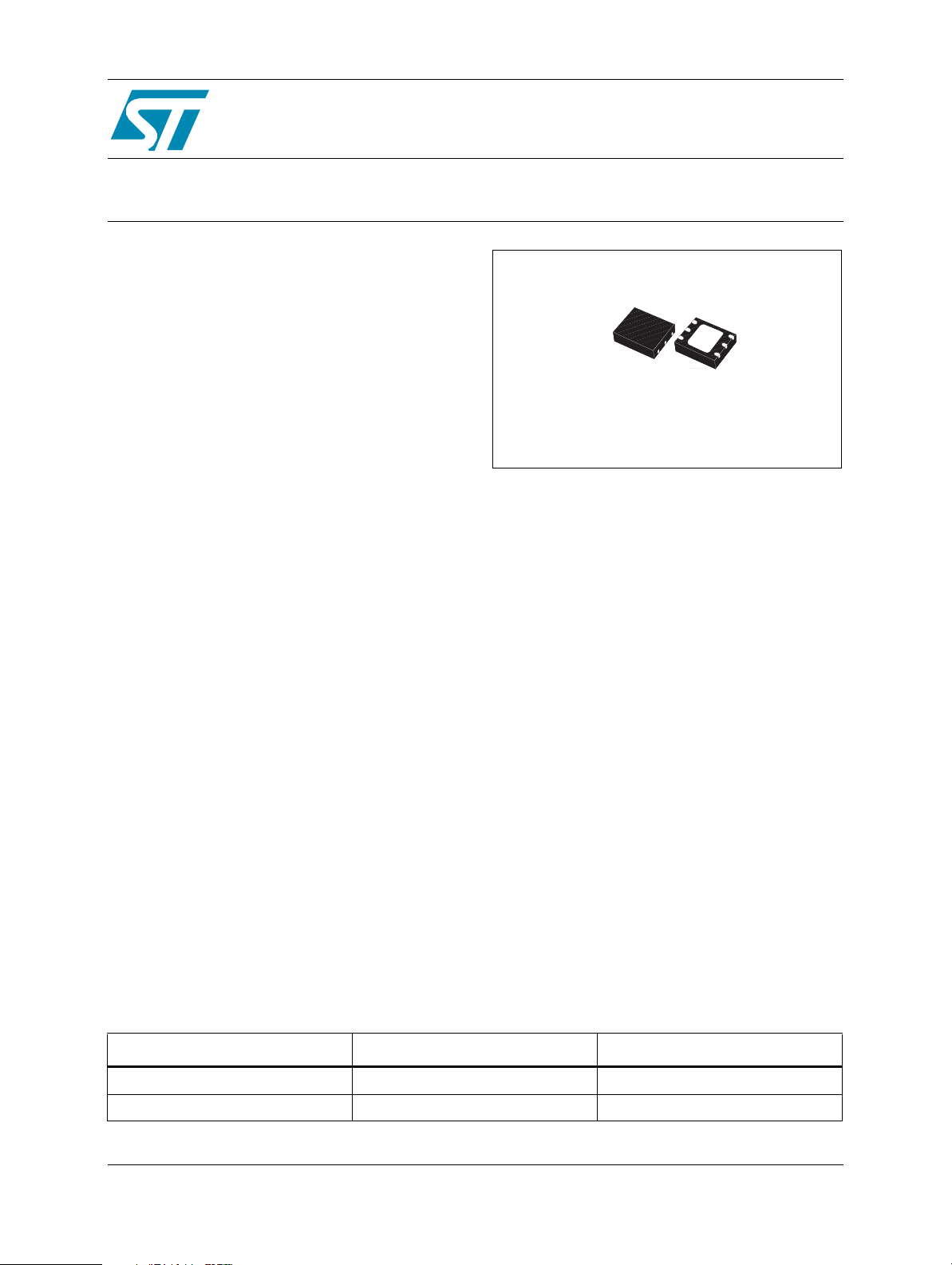
ST1S03A
step-down switching regulator
DFN6D (3x3 mm)
Description
The ST1S03A is a step down DC-DC converter
optimized for powering low-voltage digital core in
HDD applications and, generally, to replace the
high current linear solution when the power
dissipation may cause an high heating of the
application environment. It provides up to 1.5 A
over an input voltage range of 3 V to 5.5 V. An high
switching frequency (1.5 MHz) allows the use of
tiny surface-mount components: as well as the
resistor divider to set the output voltage value,
only an inductor, a schottky diode and two
capacitors are required. Besides, a low output
ripple is guaranteed by the current mode PWM
topology and by the use of low ESR SMD ceramic
capacitors. The device is thermal protected and
current limited to prevent damages due to
accidental short circuit. The ST1S03A is available
in DFN6D (3x3 mm).
Table 1. Device summary
Order codes Packaging Package
ST1S03APUR Tape and reel DFN6D (3x3 mm)
ST1S03AIPUR Tape and reel DFN6D (3x3 mm)
June 2008 Rev 6 1/14
www.st.com
14

ST1S03A
Contents
1 Diagram . . . . . . . . . . . . . . . . . . . . . . . . . . . . . . . . . . . . . . . . . . . . . . . . . . . . . 3
2 Pin configuration . . . . . . . . . . . . . . . . . . . . . . . . . . . . . . . . . . . . . . . . . . . . . 4
3 Maximum ratings . . . . . . . . . . . . . . . . . . . . . . . . . . . . . . . . . . . . . . . . . . . . . . 5
4 Electrical characteristics . . . . . . . . . . . . . . . . . . . . . . . . . . . . . . . . . . . . . . . 6
5 Typical application . . . . . . . . . . . . . . . . . . . . . . . . . . . . . . . . . . . . . . . . . . . . 7
6 Application notes . . . . . . . . . . . . . . . . . . . . . . . . . . . . . . . . . . . . . . . . . . . . . 8
7 Package mechanical data . . . . . . . . . . . . . . . . . . . . . . . . . . . . . . . . . . . . . . . 9
8 Revision history . . . . . . . . . . . . . . . . . . . . . . . . . . . . . . . . . . . . . . . . . . . . . . 13
2/14
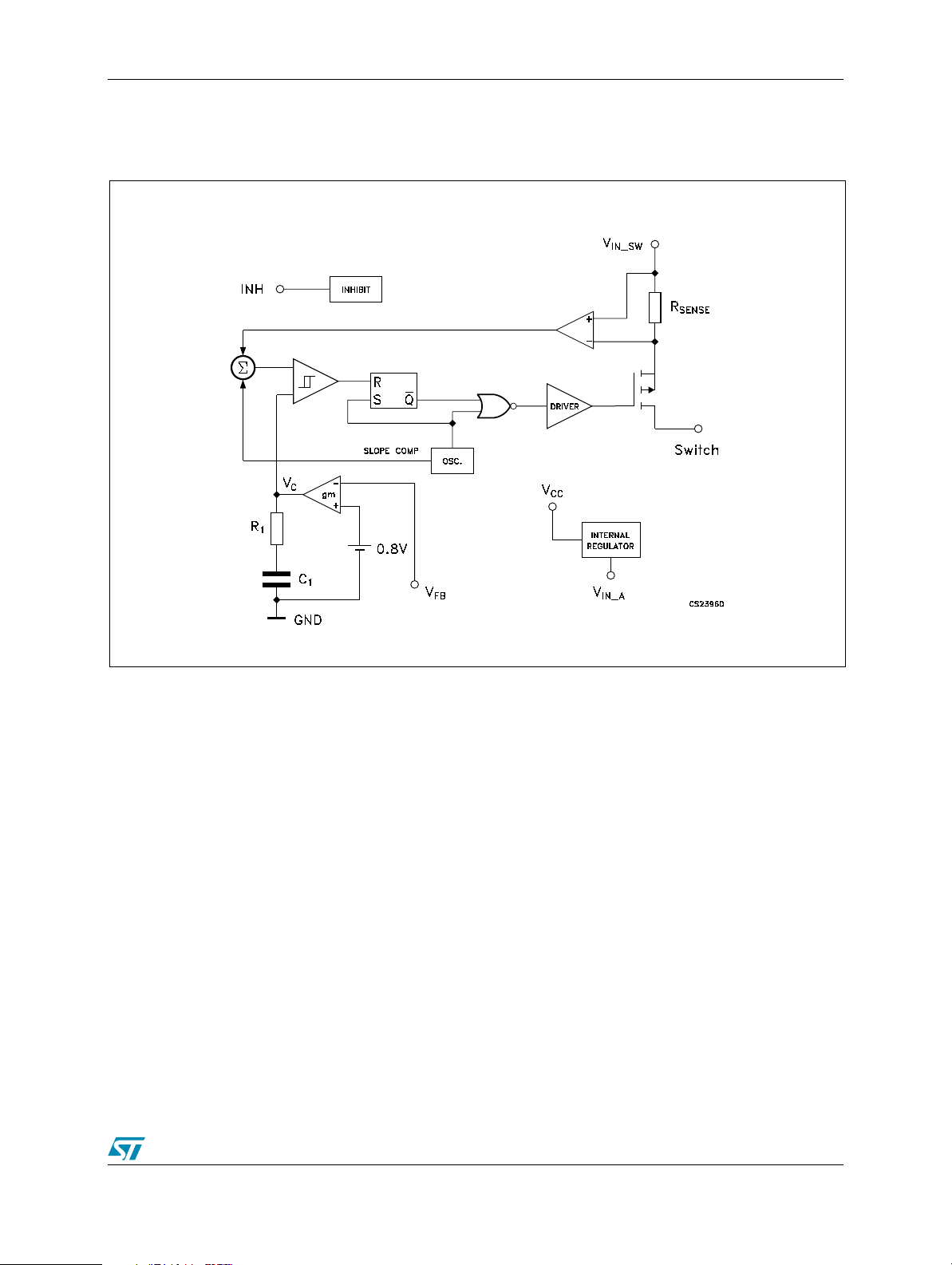
ST1S03A Diagram
1 Diagram
Figure 1. Schematic diagram
3/14
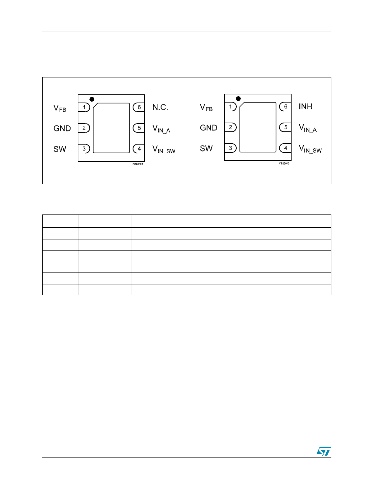
Pin configuration ST1S03A
2 Pin configuration
Figure 2. Pin configuration (top view)
ST1S03A
Table 2. Pin description
Pin n° Symbol Name and function
1
2 GND System ground
3 SW Output of the internal power switch
4
5
6 N.C./INH Not connected / or inhibit
V
V
IN_SW
V
FB
IN_A
Voltage of feedback
Power supply for the mosfet switch
Power supply for the analog circuit
ST1S03AI
4/14
ST1S03A Maximum ratings
3 Maximum ratings
Table 3. Absolute maximum ratings
Symbol Parameter Value Unit
V
IN_SW
V
IN_A
V
INH
SWITCH
Voltage
V
FB
I
VFB
T
J
T
STG
T
LEAD
Positive power supply voltage -0.3 to 7 V
Positive power supply voltage -0.3 to 7 V
Max voltage of inhibit pin -0.3 to 6 V
Max voltage of output pin -0.3 to 7 V
Feedback voltage 2.5 V
Common mode input voltage 1 mA
Max junction temperature 150 °C
Storage temperature range -25 to 150 °C
Lead temperature (soldering) 10 sec 300 °C
Note: Absolute maximum ratings are those values beyond which damage to the device may occur.
Functional operation under these conditions is not implied.
Table 4. Thermal data
Symbol Parameter Value Unit
R
thJA
R
thJC
Thermal resistance junction-ambient 55 °C/W
Thermal resistance junction-case 10 °C/W
5/14

Electrical characteristics ST1S03A
4 Electrical characteristics
Table 5. Electrical characteristics
(V
IN_SW
= V
IN_A
= V
= 5 V, CI = 4.7 µF, CO = 22 µF, L1 = 3.3 µH, TJ = 0 to 125 °C (unless
INH
otherwise specified. Typical values are referred to 25 °C)
Symbol Parameter Test conditions Min. Typ. Max. Unit
FB Feedback voltage 784 800 816 mV
I
FB
I
V
INH
I
I
MIN
%V
O
%VO/ΔI
PWMf
D
MAX
I
SW
V
ν Efficiency
T
SHDN
T
HYS
%V
O
%VO/ΔI
@
=Short
I
O
VFB pin bias current
> 1.2V
V
Quiescent current
Q
V
INH
INH
< 0.4V
Device ON 1.2
Inhibit threshold
Device OFF 0.4
O
Output current
V
I
1.5 A
= 2.7 to 5.5V
Minimum output current 1 mA
/ΔV
Reference line regulation
I
Reference load regulation
O
PWM switching frequency
S
Maximum duty cycle
= 2.7V to 5.5V
V
I
I
= 10mA to 1.5A
O
= 0.7V, TA = 25°C Note 1
V
FB
V
= 0.7V
FB
0.2
0.2
1.2 1.5 1.8 MHz
87 %
Switching current limitation 2.5 A
DS
Switch V
DS
I
= 800mA
SW
I
= 10mA to 100mA, VO = 3.3V
O
I
= 100mA to 1.5A, VO = 3.3V
O
70
85
Thermal shutdown Note 1 130 150 °C
Thermal shutdown hysteresis Note 1 15 °C
= 100mA to 1.5A, TA = 25°C
I
/ΔI
Load transient response
O
O
Short circuit removal response
O
= tF ≥ 100ns, Note 1
t
R
I
= 10mA to short, TA = 25°C
O
Note 1
-3 +3
-10 +10
600 nA
1.5 mA
1µA
V
%VO/
ΔV
%V
ΔI
200 mV
%
%V
%V
I
/
O
O
O
O
Note: 1 Guaranteed by design, but not tested in production
6/14

ST1S03A Typical application
5 Typical application
Figure 3. Application circuits
7/14

Application notes ST1S03A
6 Application notes
The ST1S03A is an adjustable current mode PWM step-down DC-DC converter with internal
1.5 A power switch, packaged in a 6-lead DFN 3x3 mm.
It’s a complete 1.5 A switching regulator with its internal compensation eliminating additional
component.
The constant frequency, current mode, PWM architecture and stable operation with ceramic
capacitors results in low, predictable output ripple. However, in order to maximize the power
conversion efficiency with light load, the regulator reduces automatically the switching
frequency when the output load becomes less than 250 mA typically.
To clamp the error amplifier reference voltage a soft start control block generating a voltage
ramp, has been implemented. Besides an on-chip power on reset of 50 = 100 µs ensure the
proper operation when switching on the power supply. other circuits fitted to the device
protection are the thermal shutdown block which turn off the regulator when the junction
temperature exceeds 150 °C typically and the cycle-by-cycle current limiting that provides
protection against shorted outputs.
Being the ST1S03A an adjustable regulator, the output voltage is determined by an external
resistor divider. The desired value is given by the following equation:
V
= V
O
To make the device working, only other four external components are required: an inductor a
schottky and two capacitors. The chosen inductor must be able to not saturate at the peak
current level. Besides, its value can be selected keeping in account that a large inductor value
increases the efficiency at low output current and reduces output voltage ripple, while a smaller
inductor can be chosen when it is important to reduce the package size and the total cost of the
application. Finally, the ST1S03A has been designed to work properly with X5R or X7R SMD
ceramic capacitors both at the input and at the output this kind of capacitors, thanks to their
very low series resistance (ESR), minimize the output voltage ripple. Other low ESR capacitors
can be used according to the need of the application without invalidate the right functioning of
the device.
Due to the high switching frequency and peak current, it is important to optimize the application
environment reducing the length of the PCB traces and placing all the external component near
the device.
[1 + R1 / R2]
FB
8/14

ST1S03A Package mechanical data
7 Package mechanical data
In order to meet environmental requirements, ST offers these devices in ECOPACK® packages.
These packages have a lead-free second level interconnect. The category of second Level
Interconnect is marked on the package and on the inner box label, in compliance with JEDEC
Standard JESD97. The maximum ratings related to soldering conditions are also marked on
the inner box label. ECOPACK is an ST trademark. ECOPACK specifications are available at:
www.st.com.
9/14
Package mechanical data ST1S03A
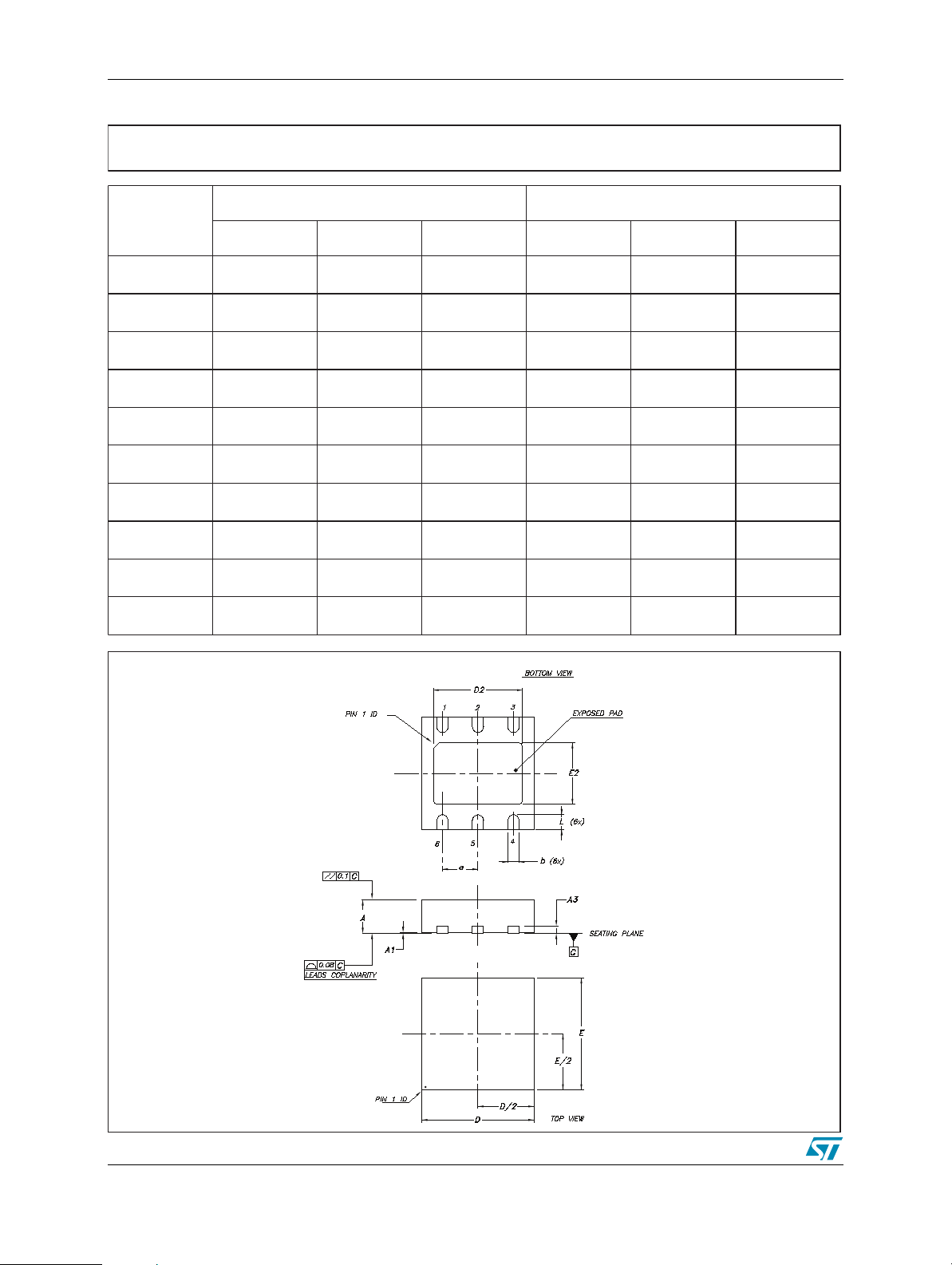
DFN6D (3x3 mm) mechanical data
mm. inch.
Dim.
Min. Typ. Max. Min. Typ. Max.
A0.80 1.00 0.031 0.039
A1 0 0.02 0.05 0 0.001 0.002
A3 0.20 0.008
b 0.23 0.45 0.009 0.018
D2.90 3.00 3.10 0.114 0.118 0.122
D2 2.23 2.50 0.088 0.098
E2.90 3.00 3.10 0.114 0.118 0.122
E2 1.50 1.75 0.059 0.069
e0.950.037
L0.30 0.40 0.50 0.012 0.016 0.020
10/14
7946637B

ST1S03A Package mechanical data
Tape & Reel QFNxx/DFNxx (3x3) Mechanical Data
mm. inch.
Dim.
Min. Typ. Max. Min. Typ. Max.
A 330 12.992
C 12.8 13.2 0.504 0.519
D 20.2 0.795
N60 2.362
T18.4 0.724
Ao 3.3 0.130
Bo 3.3 0.130
Ko 1.1 0.043
Po 4 0.157
P 8 0.315
11/14

Package mechanical data ST1S03A
Figure 4. DFN6 (3x3 mm) footprint recommended data
12/14

ST1S03A Revision history
8 Revision history
Table 6. Document revision history
Date Revision Changes
04-May-2006 1 First release.
06-Jun-2006 2 Ta bl e 3 has been updated.
29-May-2007 3 Add new mechanical data DFN6D and order codes updated.
12-Mar-2008 4 Added: Table 1 on page 1 and Figure 4 on page 12.
16-May-2008 5 Modified: Table 4 on page 5.
03-Jun-2008 6 Modified: Table 5 on page 6.
13/14

ST1S03A
Please Read Carefully:
Information in this document is provided solely in connection with ST products. STMicroelectronics NV and its subsidiaries (“ST”) reserve the
right to make changes, corrections, modifications or improvements, to this document, and the products and services described herein at any
time, without notice.
All ST products are sold pursuant to ST’s terms and conditions of sale.
Purchasers are solely responsible for the choice, selection and use of the ST products and services described herein, and ST assumes no
liability whatsoever relating to the choice, selection or use of the ST products and services described herein.
No license, express or implied, by estoppel or otherwise, to any intellectual property rights is granted under this document. If any part of this
document refers to any third party products or services it shall not be deemed a license grant by ST for the use of such third party products
or services, or any intellectual property contained therein or considered as a warranty covering the use in any manner whatsoever of such
third party products or services or any intellectual property contained therein.
UNLESS OTHERWISE SET FORTH IN ST’S TERMS AND CONDITIONS OF SALE ST DISCLAIMS ANY EXPRESS OR IMPLIED
WARRANTY WITH RESPECT TO THE USE AND/OR SALE OF ST PRODUCTS INCLUDING WITHOUT LIMITATION IMPLIED
WARRANTIES OF MERCHANTABILITY, FITNESS FOR A PARTICULAR PURPOSE (AND THEIR EQUIVALENTS UNDER THE LAWS
OF ANY JURISDICTION), OR INFRINGEMENT OF ANY PATENT, COPYRIGHT OR OTHER INTELLECTUAL PROPERTY RIGHT.
UNLESS EXPRESSLY APPROVED IN WRITING BY AN AUTHORIZED ST REPRESENTATIVE, ST PRODUCTS ARE NOT
RECOMMENDED, AUTHORIZED OR WARRANTED FOR USE IN MILITARY, AIR CRAFT, SPACE, LIFE SAVING, OR LIFE SUSTAINING
APPLICATIONS, NOR IN PRODUCTS OR SYSTEMS WHERE FAILURE OR MALFUNCTION MAY RESULT IN PERSONAL INJURY,
DEATH, OR SEVERE PROPERTY OR ENVIRONMENTAL DAMAGE. ST PRODUCTS WHICH ARE NOT SPECIFIED AS "AUTOMOTIVE
GRADE" MAY ONLY BE USED IN AUTOMOTIVE APPLICATIONS AT USER’S OWN RISK.
Resale of ST products with provisions different from the statements and/or technical features set forth in this document shall immediately void
any warranty granted by ST for the ST product or service described herein and shall not create or extend in any manner whatsoever, any
liability of ST.
ST and the ST logo are trademarks or registered trademarks of ST in various countries.
Information in this document supersedes and replaces all information previously supplied.
The ST logo is a registered trademark of STMicroelectronics. All other names are the property of their respective owners.
© 2008 STMicroelectronics - All rights reserved
STMicroelectronics group of companies
Australia - Belgium - Brazil - Canada - China - Czech Republic - Finland - France - Germany - Hong Kong - India - Israel - Italy - Japan -
Malaysia - Malta - Morocco - Singapore - Spain - Sweden - Switzerland - United Kingdom - United States of America
www.st.com
14/14
 Loading...