

ST ST1L05, ST1L05A, ST1L05B, ST1L05C, ST1L05D User Manual
ST1L05B - ST1L05C - ST1L05D
Very low quiescent BiCMOS voltage regulator
Features
■ Fixed output voltage: 1.8 V, 2.5 V, 3.3 V and
ADJ
■ Output voltage tolerance: ± 2 % at 25 °C
■ Output current capability: 1.3 A
■ Very low quiescent current: max 650 µA Over
temperature range
■ Typ. dropout 0.3 V (@ I
■ Enable function for the B, C and D versions
■ Power Good function for the B and D versions
■ Stable with low ESR ceramic capacitors
■ Thermal shutdown protection with hysteresis
■ Overcurrent protection
■ Operating junction temperature range: from 0
to 125 °C
Description
The ST1L05 family is a low drop linear voltage
regulator capable of supplying up to 1.3 A output
current.
=1.3 A)
O
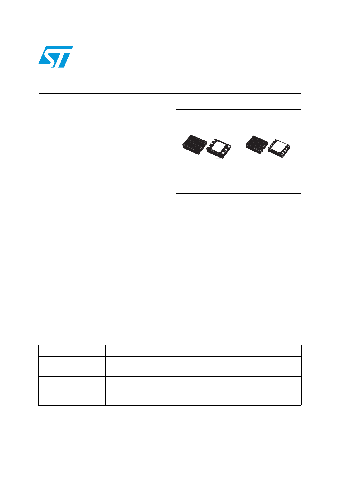
ST1L05 - ST1L05A
DFN8 (4 x 4 mm)DFN6 (3 x 3 mm)
range. The ST1L05 is stable with low ESR output
ceramic capacitors.
Internal protection circuitry includes thermal
protection with hysteresis and overcurrent limiting.
The ST1L05 is especially suitable for data storage
applications such as HDDs, where it can be used
to supply the 3.3 V required by read channel and
memory chips.
The regulator is available in the small and thin
DFN6 (3 x 3) and DFN8 (4 x 4) packages.
The output voltage is fixed at 1.8 V, 2.5 V, 3.3 V
and Adjustable. It is available in three different
versions with different pin outs.
Thanks to BiCMOS technology, the quiescent
current is controlled and maintained below 650 µA
over the entire allowed junction temperature
Table 1. Device summary
Order codes Packages Output voltages
ST1L05PU25R DFN6D (3 x 3 mm) 2.5 V
ST1L05APU33R DFN6D (3 x 3 mm) 3.3 V
September 2009 Doc ID 14492 Rev 2 1/24
ST1L05BPUR DFN6D (3 x 3 mm) ADJ
ST1L05CPU33R DFN6D (3 x 3 mm) 3.3 V
ST1L05DPUR DFN8 (4 x 4 mm) ADJ
www.st.com
24

Contents ST1L05, ST1L05A, ST1L05B, ST1L05C, ST1L05D
Contents
1 Schematic diagrams . . . . . . . . . . . . . . . . . . . . . . . . . . . . . . . . . . . . . . . . . 3
2 Pin configuration . . . . . . . . . . . . . . . . . . . . . . . . . . . . . . . . . . . . . . . . . . . . 5
3 Maximum ratings . . . . . . . . . . . . . . . . . . . . . . . . . . . . . . . . . . . . . . . . . . . . 6
4 Electrical characteristics . . . . . . . . . . . . . . . . . . . . . . . . . . . . . . . . . . . . . 7
5 Typical characteristics . . . . . . . . . . . . . . . . . . . . . . . . . . . . . . . . . . . . . . 11
6 Application information . . . . . . . . . . . . . . . . . . . . . . . . . . . . . . . . . . . . . 14
6.1 Power dissipation . . . . . . . . . . . . . . . . . . . . . . . . . . . . . . . . . . . . . . . . . . . 16
6.2 Enable function (ST1L05B, ST1L05C and ST1L05D only) . . . . . . . . . . . 16
6.3 Power Good function (ST1L05B and ST1L05D only) . . . . . . . . . . . . . . . . 16
7 Package mechanical data . . . . . . . . . . . . . . . . . . . . . . . . . . . . . . . . . . . . 17
8 Revision history . . . . . . . . . . . . . . . . . . . . . . . . . . . . . . . . . . . . . . . . . . . 23
2/24 Doc ID 14492 Rev 2

ST1L05, ST1L05A, ST1L05B, ST1L05C, ST1L05D Schematic diagrams
1 Schematic diagrams
Figure 1. Schematic diagram for ST1L05
V
V
I
I
V
V
I
I
BandGap
BandGap
reference
reference
OpAmp
OpAmp
Current
Current
limit
limit
Thermal
Thermal
protection
protection
V
V
O
O
VO_
VO_
SENSE
SENSE
R
R
1
1
R
R
2
2
Figure 2. Schematic diagram for ST1L05A
V
V
I
I
BandGap
BandGap
reference
reference
OpAmp
OpAmp
GND
GND
GND
GND
Current
Current
limit
limit
Thermal
Thermal
protection
protection
V
V
I
I
V
V
O
O
R
R
1
1
R
R
2
2
Doc ID 14492 Rev 2 3/24

Schematic diagrams ST1L05, ST1L05A, ST1L05B, ST1L05C, ST1L05D
Figure 3. Schematic diagram for ST1L05B and ST1L05D
V
V
I
EN
EN
I
BandGap
BandGap
reference
reference
Power-good
Power-good
signal
signal
Current
OpAmp
OpAmp
V
V
I
I
R
R
P
P
Internal
Internal
enable
enable
GND
GND
Current
limit
limit
Thermal
Thermal
protection
protection
PG
PG
V
V
I
I
V
V
O
O
ADJ
ADJ
Figure 4. Schematic diagram for ST1L05C
V
V
I
I
BandGap
BandGap
reference
reference
V
V
I
I
R
R
P
P
EN
EN
Internal
Internal
enable
enable
OpAmp
OpAmp
GND
GND
Current
Current
limit
limit
Thermal
Thermal
protection
protection
Power-good
Power-good
signal
signal
PG
PG
V
V
I
I
V
V
O
O
ADJ
ADJ
4/24 Doc ID 14492 Rev 2

ST1L05, ST1L05A, ST1L05B, ST1L05C, ST1L05D Pin configuration
2 Pin configuration
Figure 5. Pin connections (top through view)
ST1L05
ST1L05A
ST1L05C
Table 2. Pin description
Pin n°
Symbol
ST1L05 ST1L05A ST1L05B ST1L05C ST1L05D
V
I
V
O
6366 8
4244 6
GND 2 6 2 2 2 Ground pin
ADJ - - 5 - 7 Adjust pin
Supply voltage input pin. Bypass with a 4.7
µF capacitor to GND
Output voltage pin. Bypass with a 4.7 µF
capacitor to GND
ST1L05B
ST1L05D
Function
V
O_SENSE
5--5 -V
sense
O
PG - - 3 - 3 Power Good pin
EN - - 1 1 1 Enable pin. Internal pull-up to V
I
NC 1,3 1,4,5 - 3 4, 5 Not connected
GND EXP Exposed pad must be connected to GND
Doc ID 14492 Rev 2 5/24

Maximum ratings ST1L05, ST1L05A, ST1L05B, ST1L05C, ST1L05D
3 Maximum ratings
Table 3. Absolute maximum ratings
Symbol Parameter Value Unit
V
I
V
O
DC supply voltage -0.3 to 7 V
DC output voltage -0.3 to 7 V
PG Power Good pin -0.3 to 7 V
EN Enable pin -0.3 to 7 V
ADJ/V
OUT_SENSE
P
D
I
O
T
OP
T
STG
T
LEAD
1. Storage temperature > 125 °C are acceptable only if the regulator is soldered to a PCBA.
Adjust pin or VO sense 4 V
Power dissipation internally limited W
Output current internally limited A
Operating junction temperature range 0 to 150 °C
Storage temperature range
(1)
-65 to 150 °C
Lead temperature (soldering) 10 Sec. 260 °C
Note: Absolute maximum ratings are those values beyond which damage to the device may occur.
Functional operation under these condition is not implied.
Table 4. Thermal data
Symbol Parameter DFN6 DFN8 Unit
R
R
thJC
thJA
Thermal resistance junction-case 10 4 °C/W
Thermal resistance junction-ambient 55 40 °C/W
Table 5. ESD data
Symbol Parameter Value Unit
HBM Human body model 2 kV
MM Machine model 150 V
6/24 Doc ID 14492 Rev 2

ST1L05, ST1L05A, ST1L05B, ST1L05C, ST1L05D Electrical characteristics
4 Electrical characteristics
Refer to the typical application schematic, VI = 3.3 V to 4.5 V, IO = 5 mA to 1.3 A,
C
= CO = 4.7 µF, TJ = 0 to 125 °C, unless otherwise specified. Typical values are intended at
I
T
= 25 °C unless otherwise specified.
J
Table 6. Electrical characteristics for the ST1L05PU25
Symbol Parameter Test condition Min. Typ. Max. Unit
V
V
ΔV
ΔV
I
I
OMIN
V
I
SVR Supply voltage rejection
eN RMS output noise
ΔVO/ΔIOLoad transient (rising)
ΔVO/ΔIOLoad transient (falling)
ΔVO/ΔVIStart-up transient
ΔVO/ΔI
T
Output voltage VI =3.3V to 5.25V, T=25°C 2.45 2.5 2.55 V
O
Output voltage VI = 3.3V to 5.25V 2.4375 2.5 2.5625 V
O
Line regulation VI = 4.75V to 5.25V 15 mV
O
Load regulation VI = 4.75V, IO = 10mA to 1.3A 15 30 mV
O
Output current limit VI = 5.5V 1.3 A
S
Minimum output current for
regulation
Dropout voltage
d
Quiescent current
Q
(1)
(1)
(1)(2)
(1)(2)
(1)(2)
Short circuit removal response
(1)(2)
O
Thermal shutdown trip point
SH
(1)
1. Guaranteed by design. Not tested in production
=10µF, CO =10µF, all X7R ceramic capacitors.
2. C
I
0mA
I
= 0.8A 0.2 0.4 V
O
= 1A 0.25 0.45 V
I
O
= 1.3A 0.3 0.5 V
I
O
VI = 5V, IO = 2mA to 1.3A, T=25°C 350 500
µA
= 5.5V, IO = 2mA to 1.3A 350 650
V
I
VI = 5±0.5V, IO = 5mA, f=120Hz 50 68 dB
B = 10Hz to 10kHz, VI = 5V,
IO=5mA
VI =5V, any 200mA step from
100mA to 1.3A, t
≥ 1µs
R
0.003 %V
5%V
VI =5V, IO = 1.3A to 10mA, tF ≥ 1µs 2.75 V
VI =0V to 5V, IO = 10mA to 1.3A,
≥ 1µs
t
R
2.75 V
VI =5V, IO = short to 10mA 2.75 V
VI =5V 165 °C
O
O
Doc ID 14492 Rev 2 7/24

Electrical characteristics ST1L05, ST1L05A, ST1L05B, ST1L05C, ST1L05D
Refer to the typical application schematic, VI = 4.5 V to 5.5 V, IO = 5 mA to 1.3 A,
C
= CO = 4.7 µF, TJ = 0 to 125 °C, unless otherwise specified). Typical values are intended
I
at T
= 25 °C unless otherwise specified.
J
Table 7. Electrical characteristics for ST1L05APU33
Symbol Parameter Test condition Min. Typ. Max. Unit
V
V
ΔV
ΔV
I
I
OMIN
V
I
SVR Supply voltage rejection
eN RMS output noise
ΔVO/ΔIOLoad transient (rising)
ΔVO/ΔIOLoad transient (falling)
ΔVO/ΔVIStart-up transient
ΔV
O
T
Output voltage VI = 4.75V to 5.25V, T=25°C 3.234 3.3 3.366 V
O
Output voltage VI = 4.75V to 5.25V 3.2175 3.3 3.3825 V
O
Line regulation VI = 4.75V to 5.25V 15 mV
O
Load regulation VI = 4.75V, IO = 10mA to 1.3A 15 30 mV
O
Output current limit VI = 5.5V 1.3 A
S
Minimum output current for
regulation
Dropout voltage
d
Quiescent current
Q
(1)
(1)
(1)(2)
(1)(2)
(1)(2)
Short circuit removal response
/ΔI
(1)(2)
O
Thermal shutdown trip point
SH
( 1)
1. Guaranteed by design. Not tested in production.
=10µF, CO =10µF, all X7R ceramic capacitors.
2. C
I
0mA
I
= 0.8A 0.2 0.4 V
O
= 1A 0.25 0.45 V
I
O
I
= 1.3A 0.3 0.5 V
O
V
= 5V, IO = 2mA to 1.3A, T=25°C 350 500
I
= 5.5V, IO = 2mA to 1.3A 350 650
V
I
µA
VI = 5±0.5V, IO = 5mA, f=120Hz 50 65 dB
B = 10Hz to 10kHz, VI = 5V, IO =5mA 0.003 %V
VI =5V, any 200mA step from 100mA
to 1.3A, t
R
≥ 1µs
5%V
VI =5V, IO = 1.3A to 10mA, tF ≥ 1µs 3.6 V
VI =0V to 5V, IO = 10mA to 1.3A,
≥ 1µs
t
R
3.5 V
VI =5V, IO = short to 10mA 3.5 V
VI =5V 165 °C
O
O
8/24 Doc ID 14492 Rev 2
 Loading...