


1/186
ST10F280
March 2003
■ HIGH PERFORMANCE CPU WITH DSP FUNCTIONS
- 16-BIT CPU WITH 4-STAGE PIPELINE.
- 50ns INSTRUCTION CYCLE TIME AT 40MHz CPU
CLOCK.
- MUL TIPLY/ACCUMULATE U NIT (MAC) 16 X 16-BIT
MULTIPLICATION, 40-BIT ACCUMULATOR
- REPEAT U NI T.
- ENHANCED BOOLEAN BIT MANIPULATION FACILITIES.
- ADDITIO NA L INSTRUC T ION S TO SUPPORT HLL
AND OPERATING SYSTEMS.
- SINGLE-CYCLE CONTEXT SWITCHING SUPPORT.
■ MEMORY ORGANIZATION
- 512K BYT E ON-CHIP FL AS H MEMORY SI NG LE
VOLTAG E WITH ER AS E/ PR O GRAM CONTR O L LER.
- 100K ERASING/PROGRAMMING CYCLES.
- 20 YEAR DAT A RETENTIO N TIME
- UP TO 16M BYTE LINEAR ADDRESS SPACE FOR
CODE AND DATA (5M BYTE WITH CAN).
- 2K BYTE ON -CH IP INT ER NAL RA M (IRA M).
- 16K BYTE EXT EN SI O N RAM (XRA M ).
■ FAST AND FLEXIBLE BUS
- PROGRAMMABLE EXTERNAL BUS CHARACTERISTICS FOR DIFFERENT ADDRESS RANGES.
- 8-BIT OR 16-BIT EXTERNAL DATA BUS.
- MULTIPLEXED OR DEMULTIPLEXED EXTERNAL
ADDRESS/DATA BUSES.
- FIVE PROGRAMMABLE CHIP-SELECT SIGNALS.
- HOLD-ACKNOWLEDGE BUS ARBITRATION SUPPORT.
■ INTERRUPT
- 8-CHANNEL PERIPHERAL EVENT CONTROLLER
FOR SINGLE CYCLE, INTERRUPT DRIVEN DATA
TRANSFER.
- 16-PRIORITY-LEVEL INTERRUPT SYSTEM WITH 56
SOURCES, SAMPLE-RATE DOWN TO 25ns.
■ TWO MULTI-FUNCTIONAL GENERAL PURPOSE
TIMER UNITS WITH 5 TIMERS.
■ TWO 16-CHANNEL CAPTURE/COMPARE UNITS
■ A/D CONVERTER
- 2X16-CHANNEL 10-BIT.
- 4.85µS CONVERSION TIME
- ONE TIMER FOR ADC CHANNEL INJEC TI ON
■ 8-CHANNEL PWM UNIT
■ SERIAL CHANNELS
- SYNCHRONOUS/ASYNC SERIAL CHANNEL
- HIGH-SPEED SYNCHRONOUS CHANNEL.
■ FAIL-SAFE PROTECTIO N
- PROGRAMMABLE WATCHDOG TIMER.
- OSCILLATOR WATCHDOG.
■ TWO CAN 2.0b INTERFACES OPERATING ON ONE
OR TWO CAN BUSSES (30 OR 2X15 MESSAGE
OBJECTS)
■ ON-CHIP BOOTSTRAP LOADER
■ CLOCK GENERA TION
- ON-CHIP PL L .
- DIRECT OR PRESCALED CLOCK INPUT.
■ UP TO 143 GENERAL PUR PO SE I/O LINES
- INDIVIDUALLY PROGRAMMABLE AS INPUT, OUTPUT OR SPECIAL FUNCTION.
- PROGRAMMABLE THRESHOLD (HYSTERESIS).
■ IDLE AND POWE R DOWN M OD ES
■ MAXIMUM CP U FR EQUE NC Y 40 MH z
■ PACKAGE PBGA 208 BALLS (23mm x 23mm x
1.96 mm - PITCH 1.27mm).
■ SINGLE VOLTAGE SUPPLY: 5V ±10% (EMBEDDED
REGULATOR FOR 3.3 V CORE SUPPLY).
■ TEMPERATURE RANGE: -40 +125
°
C
PBGA208 (23 x 23 x 1.96 - Pitch 1.27 mm)
(Plastic Bold Grid Array)
ORDER CO DE: ST10F280-JT3
P4.7 CA N2_TxD
P4.6 CA N1_TxD
P4.5 CA N1_R x D
P4.4 CA N2_R x D
Port 0Port 1Port 4
Port 6
Port 5
Port 3
Port 2
GPT1
GPT2
ASC usart
BRG
CPU-Core and MAC Unit
Internal
RAM
Watchdog
Interrupt Controller
8
32 16
PEC
16
16
CAN1
Port 7 Port 8
External Bus
10-Bit ADC
BRG
SSC
PWM
CAPCOM2
CAPCOM1
16
Oscillator
Controller
16
16
512K Byte
and PLL
Flash Memory
XTAL1 XTAL2
2K Byte
15
8
8
8
16
3.3V Voltage
Regulator
16K Byte
XRAM
CAN2
XPORT916XPWM4XTIMER
P7.7 T rigge r fo r A D C
16
XPORT10
16
16
cha nnel injection
XADCINJ
External connexion
16-BIT MCU WITH MAC UNIT, 512K BYTE FLASH MEMORY AND 18K BY TE RAM
PRODUCT PREVIEW
This is advance information on a new product now in development or undergoing evaluation. Details are subject to change without notice.

ST10F280
2/186
TABLE OF CONTENTS
1 - INTRODUCTION ........... ................. ................ ........................ ................. ................... 6
2 - BALL DATA .. ................ ................. ....................... ................. ........................ ............ 7
3 - FUNCTIONAL DESCRIPTION ................ ................. ................ .......... ................ ........ 17
4 - MEMORY ORGANIZATION ....................................................................................... 18
5 - INTERNAL FLASH MEMORY ................ ................. ......... ................. ................ ........ 21
5.1 - OVERVIEW ................................................................................................................ 21
5.2 - OPERATIONAL OVERVIEW ...................................................................................... 21
5.3 - ARCHITECTURAL DESCRIPTION ............................................................................ 23
5.3.1 - Read Mode ................................................................................................................. 23
5.3.2 - Command Mode ......................................................................................................... 23
5.3.3 - Flash Status Register ................................................................................................. 23
5.3.4 - Flash Protection Register ........................................................................................... 25
5.3.5 - Instructions Description .............................................................................................. 25
5.3.6 - Reset Processing and Initial State .............................................................................. 29
5.4 - FLASH MEMORY CONFIGURATION ........................................................................ 29
5.5 - APPLICATION EXAMPLES ....................................................................................... 29
5.5.1 - Handling of Flash Addresses . ..................................................................................... 29
5.5.2 - Basic Flash Access Control ........................................................................................ 30
5.5.3 - Programming Examples ............................................................................................. 31
5.6 - BOOTSTRAP LOADER ............................................................................................ 34
5.6.1 - Entering the Bootstrap Loader .................................................................................... 34
5.6.2 - Memory Configuration After Reset ............................................................................. 35
5.6.3 - Loading the Startup Code ........................................................................................... 36
5.6.4 - Exiting Bootstrap Loader Mode .................................................................................. 36
5.6.5 - Choosing the Baud Rate for the BSL ......................................................................... 37
6 - CENTRAL PROCESSING UNIT (CPU) ..................................................................... 38
6.1 - MULTIPLIER-ACCUMULATOR UNIT (MAC) ............................................................. 39
6.1.1 - Features ..................................................................................................................... 40
6.1.1.1 - Enhanced Addressing Capab ilit ies.............................................................................. 40
6.1.1.2 - Multiply-Accumulate Unit............................................................................................. 40
6.1.1.3 - Program Control. ........................ ................. ....................... ................. ........................ 40
6.2 - INSTRUCTION SET SUMMARY ................................................................................ 41
6.3 - MAC COPROCESSOR SPECIFIC INSTRUCTIONS ................................................. 42
7 - EXTERNAL BUS CONTROLLER ............................ ......... ................. ................ ........ 46
7.1 - PROGRAMMABLE CHIP SELECT TIMING CONTROL ............................................ 46
7.2 - READY PROGRAMMABLE POLARITY ..................................................................... 47
8 - INTERRUPT SYSTEM ..... ................ ........................ ................ ........................ .......... 49
8.1 - EXTERNAL INTERRUPTS ......................................................................................... 49

ST10F280
3/186
8.2 - INTERRUPT REGISTERS AND VECTORS LOCATION LIST .................................. 50
8.3 - INTERRUPT CONTROL REGISTERS ....................................................................... 52
8.4 - EXCEPTION AND ERROR TRAPS LIST ................................................................... 53
9 - CAPTURE/COMPARE (CAPCOM) UNITS ................................................................ 54
10 - GENERAL PURPOSE TIMER UNIT .......................................................................... 57
10.1 - GPT1 .......................................................................................................................... 57
10.2 - GPT2 .......................................................................................................................... 58
11 - PWM MODULE .................. ........................ ................ ........................ ................ ........ 60
11.1 - STANDARD PWM MODULE ...................................................................................... 60
11.2 - NEW PWM MODULE : XPWM ................................................................................... 61
11.2.1 - Operating Modes ........................................................................................................62
11.2.1.1 - Mode 0: Standard PWM Generation (Edge Aligned PW M)......................................... 62
11.2.1.2 - Mode 1: Symmetrical PWM Generation (Ce nter Aligned PW M) ................................. 63
11.2.1.3 - Burst Mode ................................................................................................................ 64
11.2.1.4 - Single Shot Mode .... ........................ ................. ....................... ................. ................. 65
11.2.2 - XPWM Module Registers ........................................................................................... 66
11.2.3 - Interrupt Request Generation ..................................................................................... 68
11.2.4 - XPWM Output Signals ................................................................................................ 68
11.2.5 - XPOLAR Register (polarity of the XPWM channel) .................................................... 69
12 - PARALLEL PORTS ........... ................ ........................ ................. ....................... ........ 70
12.1 - INTRODUCTION ........................................................................................................ 72
12.1.1 - Open Drain Mode ....................................................................................................... 72
12.1.2 - Input Threshold Control ............................................................................................ 73
12.1.3 - Output Driver Control ................................................................................................73
12.1.4 - Alternate Port Functions ............................................................................................. 75
12.2 - PORT0 ........................................................................................................................ 76
12.2.1 - Alternate Functions of PORT0 .................................................................................... 77
12.3 - PORT1 ........................................................................................................................ 79
12.3.1 - Alternate Functions of PORT1 .................................................................................... 79
12.4 - PORT 2 ....................................................................................................................... 80
12.4.1 - Alternate Functions of Port 2 ..................................................................................... 81
12.5 - PORT 3 ....................................................................................................................... 84
12.5.1 - Alternate Functions of Port 3 ...................................................................................... 85
12.6 - PORT 4 ....................................................................................................................... 87
12.6.1 - Alternate Functions of Port 4 ...................................................................................... 88
12.7 - PORT 5 ....................................................................................................................... 92
12.7.1 - Port 5 Schmitt Trigger Analog Inputs .......................................................................... 93
12.8 - PORT 6 ....................................................................................................................... 93
12.8.1 - Alternate Functions of Port 6 ...................................................................................... 94
12.9 - PORT 7 ....................................................................................................................... 95
12.9.1 - Alternate Functions of Port 7 ...................................................................................... 96

ST10F280
4/186
12.10 - PORT 8 .......... ................ ................. ....................... ................. ........................ ............ 99
12.10.1 - Alternate Functions of Port 8 ...................................................................................... 99
12.11 - XPORT 9 .................................................................................................................... 101
12.12 - XPORT 10 .................................................................................................................. 103
12.12.1 - Alternate Functions of XPort 10 .................................................................................. 103
12.12.2 - New Disturb Protection on Analog Inputs ................................. ....... ..... ....... ....... ..... ... 104
13 - A/D CONVERTER ................... ....................... ................. ........................ ................ ... 105
13.1 - A/D CONVERTER MODULE ...................................................................................... 105
13.2 - MULTIPLEXAGE OF TWO BLOCKS OF 16 ANALOG INPUTS ................................ 106
13.3 - XTIMER PERIPHERAL (TRIGGER FOR ADC CHANNEL INJECTION) ................... 107
13.3.1 - Main Features ............................................................................................................. 107
13.3.2 - Register Description ...................................................................................................108
13.3.2.1 - TCR : Timer Control Register...................................................................................... 108
13.3.2.2 - XTSVR :Timer Start Value Register............................................................................ 109
13.3.2.3 - XTEVR : Timer End Value Regist e r.............. ........................ ................ ...................... 109
13.3.2.4 - XTCVR : Timer Current Value Register....................................................................... 109
13.3.2.5 - Registers Mapping....................................................................................................... 109
13.3.3 - Block Diagram ........................................................................................................... 110
13.3.3.1 - C l o cks........ ................ ........................ ................. ....................... ................. ....... .......... 110
13.3.3.2 - R e g i ste r s........ ....................... ................. ........................ ................ ............................. 110
13.3.3.3 - Timer output (XADCINJ).............................................................................................. 111
14 - SERIAL CHANNELS .............. ................ ........................ ........................ ................ ... 112
14.1 - ASYNCHRONOUS / SYNCHRONOUS SERIAL INTERFACE (ASCO) .................... 112
14.1.1 - ASCO in Asynchronous Mode .................................................................................... 112
14.1.2 - ASCO in Synchronous Mode ...................................................................................... 114
14.2 - HIGH SPEED SYNCHRONOUS SERIAL CHANNEL (SSC) .......... .......... ................. 116
15 - CAN MODULES ... ................ ........................ ................. ................ ........................ ..... 118
15.1 - MEMORY MAPPING .................................................................................................. 1 18
15.1.1 - CAN1 .......................................................................................................................... 118
15.1.2 - CAN2 .......................................................................................................................... 118
15.2 - CAN BUS CONFIGURATIONS .................................................................................. 118
15.3 - REGISTER AND MESSAGE OBJECT ORGANIZ AT IO N ........................... ............... 119
15.4 - CAN INTERRUPT HANDLING ................................................................................. 121
15.5 - THE MESSAGE OBJECT .......................................................................................... 124
15.6 - ARBITRATION REGISTERS ...................................................................................... 126
16 - WATCHDOG TIMER ............................. ................ ................. ........................ ............ 127
17 - SYSTEM RESET ........................................................................................................ 129
17.1 - ASYNCHRONOUS RESET (LONG HARDWARE RESET) ....................................... 129
17.2 - SYNCHRONOUS RESET (WARM RESET) .............................................................. 130

ST10F280
5/186
17.3 - SOFTWARE RESET .................................................................................................. 131
17.4 - WATCHDOG TIMER RESET ..................................................................................... 131
17.5 - RSTOUT PIN AND BIDIRECTIONAL RESET ............................................................ 131
17.6 - RESET CIRCUITRY ................................................................................................... 132
18 - POWER REDUCTION MODES ................................................................................. 135
18.1 - IDLE MODE ................................................................................................................135
18.2 - POWER DOWN MODE .............................................................................................. 135
18.2.1 - Protected Power Down Mode ..................................................................................... 136
18.2.2 - In terruptable Power Down Mode ................................................................................ 136
19 - SPECIAL FUNCTION REGISTER OVERVIEW ......................................................... 139
19.1 - IDENTIFICATION REGISTERS ................................................................................. 148
19.2 - SYSTEM CONFIGURATION REGISTERS ................................................................ 149
20 - ELECTRICAL CHARACTERISTICS ............. ................. ................ .......... ................. 155
20.1 - ABSOLUTE MAXIMUM RATINGS ............................................................................. 155
20.2 - PARAMETER INTERPRETATION ............................................................................. 155
20.3 - DC CHARACTERISTICS ........................................................................................... 155
20.3.1 - A/D Converter Characteristics .................................................................................... 158
20.3.2 - Conversion Timing Control ....................................................................................... 159
20.4 - AC CHARACTERISTICS ............................................................................................ 160
20.4.1 - Test Waveforms .......................................................................................................160
20.4.2 - Definition of Internal Timing ........................................................................................ 160
20.4.3 - Clock Generation Modes ............................................................................................ 1 61
20.4.4 - Prescaler Operation ....................................................................................................162
20.4.5 - Direct Drive ................................................................................................................. 162
20.4.6 - Osc illator Watchdog (OW D ) ....................................................................................... 162
20.4.7 - Phase Locked Loop .................................................................................................... 162
20.4.8 - External Clock Drive XTAL1 ....................................................................................... 163
20.4.9 - Memory Cycle Variables ............................................................................................. 164
20.4.10 - Multiplexed Bus .......................................................................................................... 165
20.4.11 - Demultiplexed Bus ...................................................................................................... 171
20.4.12 - CLKOUT and READY ................................................................................................. 177
20.4.13 - External Bus Arbitration ..............................................................................................179
20.4.14 - High-Speed Synchronous Serial Interface (SSC) Timing ........................................... 181
20.4.14.1 Master Mode................................................................................................................ 181
20.4.14.2 Slave mode.................................................................................................................. 182
21 - PACKAGE MECHANICAL DATA ...................... .......... ................ .......... ................. 183
22 - ORDERING INFORMATION ...................................................................................... 1 84
ST10F280
6/186
1 - INTRODUCTION
The ST10F280 is a new derivative of the ST
Microelectronics ST10 family of 16-bit single-chi p
CMOS microcontrollers. It combines high CPU
performance (up to 20 million instructions per
second) with high peripheral functionality and
enhanced I/O-capabilities. It also provides on-chip
high-speed single voltage FLASH memory,
on-chip high-speed RAM, and clock generation
via PLL.
ST10F280 is processed in 0.35µm CMOS
technology. The MCU core and the logic is
supplied with a 5V to 3.3V on chip voltage
regulator. The part is supplied with a single 5V
supply and I/Os work at 5V .
The device is upward compatible with the
ST10F269 device, with the following set of
differences:
– Two supply pins (DC1,DC2) on the PBGA-208
package are used for decoupling the internally
generated 3.3V core logic supply. Do not connect these two pins to 5. 0V external suppl y. Instead, these pins should be connected to a
decoupling capacitor (ceramic type, value
≥ 330nF).
– The A/D Converter characteristics stay identical
but 16 new input channel are added. A bit in a
new register (XADCMUX) control the multiplexage between the first b lock of 16 channel (on
Port5) and the second block (on XPort10). The
conversion result registers stay identical and the
software management can determine the block
in use. A new dedicated timer controls now the
ADC channel injection mode on the inp ut CC 31
(P7.7). The output of this timer is visible on a
dedicated pin (XADCINJ) to emulate this new
functionnality.
– A second XPWM peripheral (4 new channels) is
added. Four dedicated pins are reserved for the
outputs (XPWM[0:3])
– A new general purpose I/O port named XPORT9
(16 bits) is added. Due to the bit addressing
management, it will be different from other
standard general purpose I/O ports.
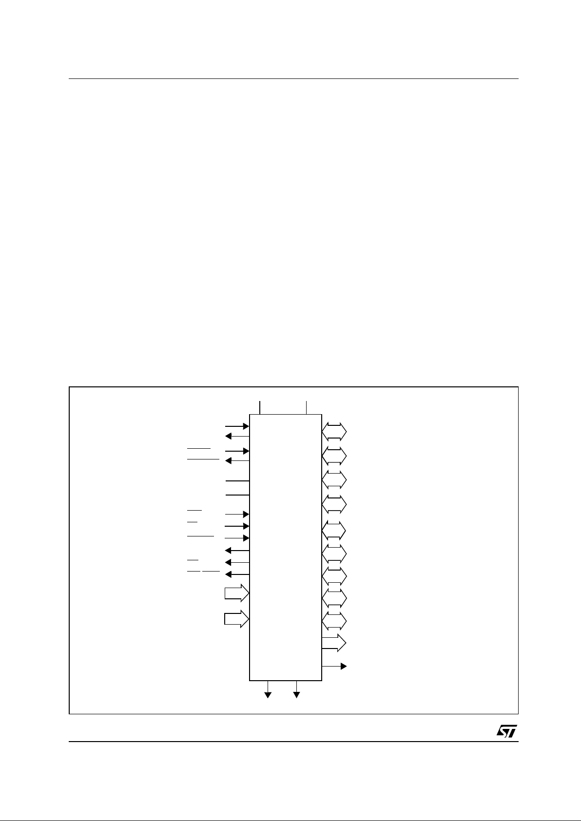
Figure 1 : Logic Symbol
XTAL1
RSTIN
XTAL2
RSTOUT
NMI
EA
READY
ALE
RD
WR/WRL
Port 5
16-bit
Port 6
8-bit
Port 4
8-bit
Port 3
15-bit
Port 2
16-bit
Port 1
16-bit
Port 0
16-bit
V
DD
V
SS
Port 7
8-bit
Port 8
8-bit
V
AREF
V
AGND
XPort 9
16-bit
XPWM
4-bit
XADCINJ
XPort10
16-bit
DC1
DC2
Decoupling capacitor for internal regulator
ST10F280
ST10F280
7/186
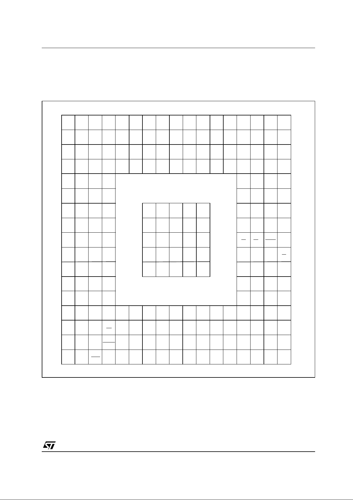
2 - BALL DATA
The ST10F280 package is a PB GA of 23 x 23 x 1.96 mm . The pitch of the balls is 1. 27 mm. The s ignal
assignment of the 208 balls is described in Figure 2 for the configuration and in Tabl e 1 for the ball signal
assignment. This package has 25 additional therm al balls.
Figure 2 : Ball Configuration (bottom view)
K7
V
SS
K8
V
SS
K9
V
SS
J7
V
SS
J8
V
SS
J9
V
SS
H7
V
SS
H8
V
SS
H9
V
SS
G7
V
SS
G8
V
SS
G9
V
SS
K10
V
SS
K11
V
SS
J10
V
SS
J11
V
SS
H10
V
SS
H11
V
SS
G10
V
SS
G11
V
SS
VSSVSSVSSVSSV
SS
U1 U2
V
AREF
U3
V
AGND
U4 U5 U6 U7 U8 U9 U1 0
V
SS
U11
DC2
U12 U13 U14 U15 U16
T1 T2 T3 T4 T5 T6 T7 T8 T9 T10 T11 T12 T13 T14 T15 T16
R1 R2 R3
R4
R14 R15 R16
M1 M2 M3
M15 M16 M17
L1
V
SS
L2 L3
L15 L16 L17
V
DD
K1
V
DD
K2 K3
K15 K16 K17
V
SS
J1 J2 J3
J15 J16 J17
H1 H2 H3
H15 H16 H17
G1 G2 G3
G15 G16 G17
F1 F2 F3
F15 F16 F17
E1 E2 E3
E15 E16 E17
V
SS
D1 D2 D3
D15 D16 D17
C1 C2 C3 C4 C5 C6 C7 C8 C9 C10 C1 1 C12 C13 C14 C15 C16
B1 B2 B3 B4 B5 B6 B7 B8 B9 B10 B11 B12 B13 B14 B15 B16
A1 A2 A3 A4
RSTIN
A5
XTAL1A6XTAL2
A7 A8 A9 A10 A11 A12 A13 A14 A15 A16
A
B
C
D
E
F
G
H
J
K
L
M
N
P
R
T
A
B
C
D
E
F
G
H
J
K
L
M
N
P
R
T
1716151413121110987654321
1716151413121110987654321
U17
T17
R17
C17
B17
A17
U
U
V
SS
DC1 V
DD
M4
L4
K4
J4
H4
G4
E4
D4
M14
L14
K14
J14
H14
G14
E14
D14
P15 P16 P17
P14
D5 D6 D7 D8 D9 D10 D11 D12 D13
P5 P6 P7 P8 P9 P10 P11 P12 P13
N1 N2 N3
N4
F4
F14
L7 L8 L9 L10 L11
V
DD
V
DD
V
SS
V
DD
V
SS
V
DD
V
SS
V
DD
V
SS
VSSV
DD
VSSV
DD
P3.15
V
DD
V
SS
RPD
XP10.3 XP10.2 XP10.1 XP10.0
XP10.4XP10.5XP10.6XP10.7
XP10.11 XP10.8 P5.6 P5.10 P5.14XP10.9XP10.10
XP10.13 XP10.12 P5.1 P5.3 P5.7 P5.11 P5.15
XP10.14 P5.0 P5.2 P5.4 P5.8 P5.12
XP10.15 P5.5 P5.9 P5.13
xpwm.0
xpwm.1
xpwm.2
xpwm.3
P6.0
P6.1
P6.2
P6.3
P6.4
P6.5
P6.6
P6.7
P8.0
P8.1P8.2
P8.3P8.4
P8.5P8.6P8.7
P7.0P7.1P7.2P7.3
P7.4 P7.5 P7.6
P7.7 XADCINJ
P2.0
P2.1
P2.2
P2.3 P2.4
P2.5
P2.6
P2.7
P2.8
P2.9
P2.10
P2.11
P2.12
P2.13
P2.14
P2.15
P3.0
P3.1
P3.2
P3.3
P3.4
P3.5
P3.6
P3.7
P3.8 P3.9
P3.10
P3.11 P3.12
P3.13
P4.0
P4.1
P4.2
P4.3
P4.4 P4.5
P4.6 P4.7
RD WR READY ALE
EAP0.0P0.1P0.2
P0.3P0.4P0.5
P0.6
P0.7
P0.8
P0.9
P0.10
P0.11
P0.12
P0.13
P0.14
P0.15
XP9.0
XP9.1
XP9.2
XP9.3
XP9.4
XP9.5
XP9.6
XP9.7
XP9.8
XP9.9
XP9.10
XP9.11
XP9.12
XP9.13
XP9.14
XP9.15
P1.0
P1.1
P1.2
P1.3
P1.4
P1.5
P1.6
P1.7P1.8
P1.9
P1.10
P1.11
P1.12
P1.13
P1.14 P1.15
V
SS
RSTOUT
NMI
V
SS
V
SS
V
SS
VSSV
SS
VSSV
SS
V
SS
V
SS
V
SS
V
SS
VSSV
SS
V
SS
V
SS
V
SS
VSSV
SS
V
SS
V
SSVSS
R5 R6 R7 R8 R9 R10 R11 R12 R13
N15 N16 N17
N14
P1 P2 P3 P4

ST10F280
8/186
Table 1 : Ball Descri pti o n
Symbol
Ball
Number
Type Function
P6.0 – P6.7 I/O Port 6 is an 8 -bit bidirectional I/O port. It is bit-wise programmable for input or
output via direction bits. For a pin configured as input, the output driver is put into
high-impedance state. Port 6 outputs can be configured as push/pull or open
drain drivers.
The following Port 6 pins also serve for alternate functions:
E4 O P6.0 CS0
Chip Select 0 Output
D3 O P6.1 CS1 Chip Select 1 Output
B1 O P6.2 CS2
Chip Select 2 Output
C1 O P6.3 CS3 Chip Select 3 Output
D2 O P6.4 CS4
Chip Select 4 Output
E3 I P6.5 HOLD External Master Hold Request Input
F4 O P6.6 HLDA
Hold Acknowledge Output
D1 O P6.7 BREQ Bus Request Output
P8.0 – P8.7 I/O Port 8 is an 8 -bit bidirectional I/O port. It is bit-wise programmable for input or
output via direction bits. For a pin configured as input, the output driver is put into
high-impedance state. Port 8 outputs can be configured as push/pull or open
drain drivers. The input threshold of Port 8 is selectable (TTL or special).
The following Port 8 pins also serve for alternate functions:
E2 I/O P8.0 CC16IO CAPCOM2: CC16 Capture Input / Compare Output
F3 I/O P8.1 CC17IO CAPCOM2: CC17 Capture Input / Compare Output
F2 I/O P8.2 CC18IO CAPCOM2: CC18 Capture Input / Compare Output
G3 I/O P8.3 CC19IO CAPCOM2: CC19 Capture Input / Compare Output
G2 I/O P8.4 CC20IO CAPCOM2: CC20 Capture Input / Compare Output
H4 I/O P8.5 CC21IO CAPCOM2: CC21 Capture Input / Compare Output
H3 I/O P8.6 CC22IO CAPCOM2: CC22 Capture Input / Compare Output
H2 I/O P8.7 CC23IO CAPCOM2: CC23 Capture Input / Compare Output
P7.0 – P7.7 I/O Port 7 is an 8 -bit bidirectional I/O port. It is bit-wise programmable for input or
output via direction bits. For a pin configured as input, the output driver is put into
high-impedance state. Port 7 outputs can be configured as push/pull or open
drain drivers. The input threshold of Port 7 is selectable (TTL or special).
The following Port 7 pins also serve for alternate functions:
J4 O P7.0 POUT0 PWM Channel 0 Output
J3 O P7.1 POUT1 PWM Channel 1 Output
J2 O P7.2 POUT2 PWM Channel 2 Output
J1 O P7.3 POUT3 PWM Channel 3 Output
K2 I/O P7.4 CC28IO CAPCOM2: CC28 Capture Input / Compare Output
K3 I/O P7.5 CC29IO CAPCOM2: CC29 Capture Input / Compare Output
K4 I/O P7.6 CC30IO CAPCOM2: CC30 Capture Input / Compare Output
L2 I/O P7.7 CC31IO CAPCOM2: CC31 Capture Input / Compare Output

ST10F280
9/186
XP10.0 – XP10.15 I XPort 10 is a 16-bit input-only port with Schmitt-Trigger characteristics.
The pins of X Port10 also serve as the analo g input c hannels (up to 16) for the
A/D converter, where XP10.X equals ANx (Analog input channel x).
M4
M3
M2
M1
N4
N3
N2
N1
P4
P3
P2
P1
R2
R1
T1
U1
I
I
I
I
I
I
I
I
I
I
I
I
I
I
I
I
XP10.0
XP10.1
XP10.2
XP10.3
XP10.4
XP10.5
XP10.6
XP10.7
XP10.8
XP10.9
XP10.10
XP10.11
XP10.12
XP10.13
XP10.14
XP10.15
P5.0 – P5.15 I Port 5 is a 16-bit input-only port with Schmitt-Trigger characteristics.
The pins of Port 5 also ser ve as the analog inp ut chann els (up to 16) for the A/D
converter, where P5.x equals ANx (Analog input channel x),
or they serve as timer inputs:
T2 I P5.0
R3 I P5.1
T3 I P5.2
R4 I P5.3
T4 I P5.4
U4 I P5.5
P5 I P5.6
R5 I P5.7
T5 I P5.8
U5 I P5.9
P6 I P5.10 T6EUD GPT2 Timer T6 External Up / Down Control Input
R6 I P5.11 T5EUD GPT2 Timer T5 External Up / Down Control Input
T6 I P5.12 T6IN GPT2 Timer T6 Count Input
U6 I P5.13 T5IN GPT2 Timer T5 Count Input
P7 I P5.14 T4EUD GPT1 Timer T4 External Up / Down Control Input
R7 I P5.15 T2EUD GPT1 Timer T2 External Up / Down Control Input
Table 1 : Ball Description (continued)
Symbol
Ball
Number
Type Function

ST10F280
10/186
P2.0 – P2.15 I/O Port 2 is a 16 -bit bidirectional I/O port. It is bit-wise programmable for input or
output via direction bits. For a pin configured as input, the output driver is put into
high-impedance state. Port 2 outputs can be configured as push/pull or open
drain drivers. The input threshold of Port 2 is selectable (TTL or special).
The following Port 2 pins also serve for alternate functions:
T7 I/O P2.0 CC0IO CAPCOM: CC0 Capture Input / Compare Output
P8 I/O P2.1 CC1IO CAPCOM: CC1 Capture Input / Compare Output
R8 I/O P2.2 CC2IO CAPCOM: CC2 Capture Input / Compare Output
T8 I/O P2.3 CC3IO CAPCOM: CC3 Capture Input / Compare Output
T9 I/O P2.4 CC4IO CAPCOM: CC4 Capture Input / Compare Output
P9 I/O P2.5 CC5IO CAPCOM: CC5 Capture Input / Compare Output
R9 I/O P2.6 CC6IO CAPCOM: CC6 Capture Input / Compare Output
U9 I/O P2.7 CC7IO CAPCOM: CC7 Capture Input / Compare Output
T10 I/OIP2.8 CC8IO CAPCOM: CC8 Capture Input / Compare Output,
EX0IN Fast External Interrupt 0 Input
R10 I/OIP2.9 CC9IO CAPCOM: CC9 Capture Input / Compare Output,
EX1IN Fast External Interrupt 1 Input
P10 I/OIP2.10 CC10IO CAPCOM: CC10 Capture Input / Compare Output,
EX2IN Fast External Interrupt 2 Input
T11 I/OIP2.11 CC11IO CAPCOM: CC11 Capture Input / Compare Output,
EX3IN Fast External Interrupt 3 Input
R11 I/OIP2.12 CC12IO CAPCOM: CC12 Capture Input / Compare Output,
EX4IN Fast External Interrupt 4 Input
U12 I/OIP2.13 CC13IO CAPCOM: CC13 Capture Input / Compare Output,
EX5IN Fast External Interrupt 5 Input
P11 I/OIP2.14 CC14IO CAPCOM: CC14 Capture Input / Compare Output,
EX6IN Fast External Interrupt 6 Input
T12 I/O
I
I
P2.15 CC15IO CAPCOM: CC15 Capture Input / Compare Output,
EX7IN Fast External Interrupt 7 Input
T7IN CAPCOM2 Timer T7 Count Input
Table 1 : Ball Description (continued)
Symbol
Ball
Number
Type Function

ST10F280
11/186
P3.0 - P3.13,
P3.15
I/O Port 3 is a 15-bit (P 3.14 is missi ng) bidirecti onal I/O por t. It i s bit-wise pro gram-
mable for input or output via direction bits. For a pin configured as input, the out-
put driver is put in to high-imp edance st ate. Port 3 outputs ca n be config ured as
push/pull or open drain dri vers. The input threshold of Port 3 is select able (TTL
or special).
The following Port 3 pins also serve for alternate functions:
R12 I P3.0 T0IN CAPCOM Timer T0 Count Input
T13 O P3.1 T6OUT GPT2 Timer T6 Toggle Latch Output
P12 I P3.2 CAPIN GPT2 Register CAPREL Capture Input
R13 O P3.3 T3OUT GPT1 Timer T3 Toggle Latch Output
T14 I P3.4 T3EUD GPT1 Timer T3 External Up / Down Control Input
P13 I P3.5 T4IN GPT1 Timer T4 Input for Count / Gate /
Reload / Capture
R14 I P3.6 T3IN GPT1 Timer T3 Count / Gate Input
P14 I P3.7 T2IN GPT1 Timer T2 Input for Count / Gate /
Reload / Capture
R15 I/O P3.8 MRST SSC Master-Receive / Slave-Transmit I/O
R16 I/O P3.9 MTSR SSC Master-Transmit / Slave-Receive O/I
N14 I/O P3.10 TxD0 ASC0 Clock / Data Output (Asynchronous / Synchronous)
P15 O P3.11 RxD0 ASC0 Data Input (Asynchronous) or I/O (Synchronous)
P16 O P3.12 BHE
External Memory High Byte Enable Signal,
WRH
External Memory High Byte Write Strobe
M14 I/O P3.13 SCLK SSC Master Clock Output / Slave Clock Input
T17 O P3.15 CLKOUT System Clock Output (=CPU Clock)
P4.0 – P4.7 I/O Port 4 is an 8 -bit bidirectional I/O port. It is bit-wise programmable for input or
output via direction bits. For a pin configured as input, the output driver is put into
high-impedance state. The input threshold is selectable (TTL or special).
P4.6 & P4.7 outputs can be configured as push-pull or open-drain drivers.
In case of an exter nal bus configuration, Por t 4 can be us ed to output the se g-
ment address lines:
N16 O P4.0 A16 Least Significant Segment Address Line
M15 O P4.1 A17 Segment Address Line
L14 O P4.2 A18 Segment Address Line
M16 O P4.3 A19 Segment Address Line
L15 OIP4.4 A20 Segment Address Line
CAN2_RxD CAN2 Receive Data Input
L16 OIP4.5 A21 Segment Address Line
CAN1_RxD CAN1 Receive Data Input
K14 OOP4.6 A22 Segment Address Line, CAN_TxD
CAN1_TxD CAN1 Transmit Data Output
K15 OOP4.7 A23 Most Significant Segment Address Line
CAN2_TxD CAN2 Transmit Data Output
Table 1 : Ball Description (continued)
Symbol
Ball
Number
Type Function

ST10F280
12/186
RD
J14 O External Memory Read Strobe. RD is activated for every external instruction or
data read access.
WR
/WRL J15 O External Memory Write Strobe. In WR-mode this pin is activated for every
external data write access. In WRL
-mode this pin is activated for low byte data
write accesses on a 16-bit bus, and for every data write access on an 8-bit bus.
See WRCFG in register SYSCON for mode selection.
READY/
READY
J16 I Ready Input. The active level is programmable. When the Ready function is
enabled, the selected inactive level at this pin during an external memory access
will force the insertion of memory cycle time waitstates until the pin returns to the
selected active level.
ALE J17 O Address Latch Enable Output. Can be used for latching the address into external
memory or an address latch in the multiplexed bus modes.
EA
H17 I External Access Enable pin. A low level at this pin during and after Reset forces
the ST10F280 to begin instruction execution out of external memory. A high level
forces execution out of the internal Flash Memory.
PORT0:
P0L.0 - P0L.7,
P0H.0 - P0H.7
I/O PORT0 consists of the two 8-bit bidirectional I/O ports P0L and P0H. It is bit-wise
programmable for input or output via direction bits. For a pin configured as input,
the output driver is put into high-impedance state.
In case of an externa l bus configuration, PORT0 serves as the address (A) a nd
address/data (AD) bus in multiplexed bus modes and as the data (D) bus in
demultiplexed bus modes.
Demultiplexed bus modes:
Data Path Width: 8-bit 16-bit
P0L.0 – P0L.7: D0 - D7 D0 - D7
P0H.0 – P0H.7: I/O D8 - D15
Multiplexed bus modes:
Data Path Width: 8-bit 16-bit
P0L.0 – P0L.7: AD0 - AD7 AD0 - AD7
P0H.0 – P0H.7: A8 - A15 AD8 - AD15
H16 I/O P0L.0
H15 I/O P0L.1
H14 I/O P0L.2
G16 I/O P0L.3
G15 I/O P0L.4
G14 I/O P0L.5
F16 I/O P0L.6
E17 I/O P0L.7
F15 I/O P0H.0
E16 I/O P0H.1
F14 I/O P0H.2
D17 I/O P0H.3
E15 I/O P0H.4
D16 I/O P0H.5
C17 I/O P0H.6
E14 I/O P0H.7
Table 1 : Ball Description (continued)
Symbol
Ball
Number
Type Function

ST10F280
13/186
XPORT9.0 XPORT9.15
I/O XPort 9 is a 16-bit bi directional I/O por t. It is bit- wise program mable for input or
output via direction bits. For a pin configured as input, the output driver is put into
high-impedanc e state. XPort 9 outputs ca n be configured as push/p ull or open
drain drivers.
D15 I/O XPORT9.0
C16 I/O XPORT9.1
D14 I/O XPORT9.2
C15 I/O XPORT9.3
B16 I/O XPORT9.4
D13 I/O XPORT9.5
C14 I/O XPORT9.6
B15 I/O XPORT9.7
A15 I/O XPORT9.8
B14 I/O XPORT9.9
C13 I/O XPORT9.10
D12 I/O XPORT9.11
B13 I/O XPORT9.12
C12 I/O XPORT9.13
D11 I/O XPORT9.14
B12 I/O XPORT9.15
Table 1 : Ball Description (continued)
Symbol
Ball
Number
Type Function

ST10F280
14/186
PORT1:
P1L.0 - P1L.7,
P1H.0 - P1H.7
I/O PORT1 consists of the two 8-bit bidirectional I/O ports P1L and P1H. It is bit-wise
programmable for input or output via direction bits. For a pin configured as input,
the output driver is put into high-imped ance state. PORT1 is used as the 16-bit
address bus (A) in demultiplexed bus modes and also after switching from a
demultiplexed bus mode to a multiplexed bus mode. The following PORT1 pins
also serve for alternate functions:
C11 I/O P1L.0
B11 I/O P1L.1
D10 I/O P1L.2
C10 I/O P1L.3
B10 I/O P1L.4
A10 I/O P1L.5
D9 I/O P1L.6
C9 I/O P1L.7
C8 I/O P1H.0
D8 I/O P1H.1
A7 I/O P1H.2
B7 I/O P1H.3
C7 I P1H.4 CC24IO CAPCOM2: CC24 Capture Input
D7 I P1H.5 CC25IO CAPCOM2: CC25 Capture Input
C5 I P1H.6 CC26IO CAPCOM2: CC26 Capture Input
C6 I P1H.7 CC27IO CAPCOM2: CC27 Capture Input
XTAL1 A5 I XTAL1: Input to the oscillator amplifier and input to the internal clock generator
XTAL2 A6 O XTAL2: Output of the oscillator amplifier circuit.
To clock the device from an extern al source, drive XTAL1, while leaving XTAL2
unconnected. Minimum and maximum high/low and rise/fall times specified in
the AC Characteristics must be observed.
RSTIN
A3 I Reset Input with Schmitt-Trigger characteristics. A low level at this pin for a spec-
ified duration while the oscillator is running resets the ST10F280. An internal pullup resistor permits power-on reset using only a capacitor connected to V
SS
.
In bidirectiona l re set m ode (en abled by setting bit BDR STEN in SYS CON reg ister), the RSTIN line is pulled low for the duration of the internal reset sequence.
RSTOUT B4 O Internal Reset Indicati on Output. This pin is set to a low level when the part is
executing either a hardware, a software or a watchdog timer reset. RSTOUT
remains low until the EINIT (end of initialization) instruction is executed.
NMI C4 I Non-Maskable Interrupt Input. A high to low transition at this pin causes the CPU
to vector to the NMI trap routine. If bit PWDCFG = ‘0’ in SYSCON register, when
the PWRDN (power down) in struction is executed, the NMI
pin must be low in
order to force the ST10F280 to go into p ower down mode. If NMI
is high and
PWDCFG =’0’, when PWRDN is executed, the part will continue to run in normal
mode.
If not used, pin NMI
should be pulled high externally.
Table 1 : Ball Description (continued)
Symbol
Ball
Number
Type Function

ST10F280
15/186
XPWM.0 D4 O XPWM Channel 0 Output
XPWM.1 C3 O XPWM Channel 1 Output
XPWM.2 B2 O XPWM Channel 2 Output
XPWM.3 C2 O XPWM Channel 3 Output
XADCINJ L3 O Output trigger for ADC channel injection
V
AREF
U2 - Reference voltage for the A/D converter.
V
AGND
U3 - Reference ground for the A/D converter.
RPD M17 I/O Timing pin for the return from powerdown circuit and synchronous/asynchronous
reset selection.
DC1 G1 O 3.3V Decoupling pin: a decoupling capacitor of ~330 nF must be connected
between this pin and nearest V
SS
pin.
DC2 U11 O 3.3V Decoupling pin: a decoupling capacitor of ~330 nF must be connected
between this pin and V
SS
nearest pin.
V
DD
A2
A9
A12
A14
E1
K1
U8
U15
P17
L17
G17
- Digital Supply Voltage: + 5 V during normal operation, idle mode and power
down mode
Table 1 : Ball Description (continued)
Symbol
Ball
Number
Type Function

ST10F280
16/186
V
SS
A1
A4
A8
A11
A13
A16
A17
B3
B5
B6
B8
B9
B17
D5
D6
F1
F17
G4
H1
K16
K17
L1
L4
N15
N17
R17
T15
T16
U7
U10
U13
U14
U16
U17
- Digital Ground.
Table 1 : Ball Description (continued)
Symbol
Ball
Number
Type Function

ST10F280
17/186
3 - FUNCTIONAL DESCRIPTION
The architecture of the ST10F280 combines
advantages of both RISC and CISC processors
and an advanced peripheral subsystem. The
block diagram g ives an overview of the different
on-chip components and the high bandwidth internal bus structure of the ST10F280.
Figure 3 : Block Diagram
P4.7 CAN2_TxD
P4.6 CAN1_TxD
P4.5 CAN1_RxD
P4.4 CAN2_RxD
Port 0
Port 1Port 4
Port 6
Port 5
Port 3
Port 2
GPT1
GPT2
ASC usart
BRG
CPU-Core and MAC Unit
Internal
RAM
Watch dog
Interrupt Controller
8
32 16
PEC
16
16
CAN1
Port 7
Port 8
External Bus
10-Bit ADC
BRG
SSC
PWM
CAPCOM2
CAPCOM1
16
Oscillator
Controller
16
16
512K Byte
and PLL
Flash Memory
XTAL1 XTAL2
2K Byte
15
8
8
8
16
3.3V Voltage
Regulator
16K Byte
XRAM
CAN2
XPORT916XPWM4XTIMER
P7.7 Trigger for ADC
16
XPORT10
16
16
XADCINJ
channel injection
External connexion

ST10F280
18/186
4 - MEMOR Y ORGA NI ZA T IO N
The memory space of the ST10F280 is configured
in a unified memory architecture. Code memory,
data memory, registers and I/O ports are organized within the same linear address space of
16M Bytes. The entire memory space can be
accessed bytewise or wordwise. Particular portions of the on-chip memory have additionally
been made directly bit addressable.
FLASH: 512K Bytes of on-chip single voltage
FLASH memory.
IRAM: 2K Bytes of on-chip internal RAM
(dual-port) is provided as a storage for data, system stack, general purpose register banks and
code. The register bank can con sist of up to 16
wordwide (R0 to R15) and/or bytewide (RL0, RH0,
…, RL7, RH7) general purpose registers. Base
address is 00’F600h, upper address is 00’FDFFh.
XRAM: 16K Bytes of on-chip extension RAM (single port XRA M) is provided as a storage for data,
user stack and cod e. The X RA M is a s ingle bank,
connected to the internal XBUS and are accessed
like an external memory in 16-bit demultiplexed
bus-mode without waitstate or read/write delay
(50ns access at 40MHz CPU clock). Byte and
word access is allowed.
The XRAM address range is 00’8000h - 00’BFFFh
if enabled (XPEN set bit 2 of SYSCON register-,
and XRAMEN set bit 2 of XPERCON register-). If
bit XRAMEN or XPEN is cleared, then any access
in the address range 00 ’8000h 00’BFFFh will be
directed to external memory interface, using the
BUSCONx register corresponding to address
matching ADDRSELx register
As the XRAM appears like external memory, it
cannot be used for the ST10F280’s system stack
or register banks. The XRAM is not provided for
single bit storage and therefore is not bit addressable.
SFR/ESFR: 1024 bytes (2 * 512 bytes) of address
space is reserved for the special func tion register
areas. SFRs are wordwide registers which are
used for controlling and monitoring functions of
the different on-chip units.
CAN1: Address range 00’EF00h 00’EFFFh is
reserved for the CAN1 Module access. The CAN1
is enabled by setting XPEN bit 2 of the SYSCON
register and bit 0 of the new XPERCON register.
Accesses to the CAN Module use demultiplexed
addresses and a 16-bi t data bus (byte accesses
are possible). Two waitstates give an access time
of 100 ns at 40MHz CPU clock. No tristate waitstate is used.
CAN2: Address range 00’EE00h 00’EEFFh is
reserved for the CAN2 Module access. The CAN2
is enabled by setting XPEN bit 2 of the SYSCON
register and bit 1 of the new XPERCON register.
Accesses to the CAN Module use demultiplexed
addresses and a 16-bi t data bus (byte accesses
are possible). Two waitstates give an access time
of 100 ns at 40MHz CPU clock. No tristate waitstate is used.
In order to meet the needs of designs where more
memory is required than is provided on chip, up to
16M Bytes of external RAM and/or ROM can be
connected to the microc ontroller. If one or the two
CAN modules are used, Port 4 can not be programmed to output all 8 segment address lines.
Thus, only 4 segment address li nes can be used,
reducing the external mem or y space to 5M Bytes
(1M Byte per CS
line).
XPWM: Address range 00’EC00h 00’ECFFh is
reserved for the XPWM Module access. The
XPWM is enabled by setting XPEN bit 2 of the
SYSCON register and bit 4 of the new XPERCON
register. Accesses to the XPWM Module use
demultiplexed addresses and a 16-bit data bus
(byte accesses are possible). Two waitstates give
an access time of 100 ns at 40MHz CPU clock. No
tristate waitstate is used.
XPORT9, XTIMER, XPORT10, XADCMUX :
Address range 00’C000h 00’C3FFh is reserved
for the XPORT9, XPORT10, XTIMER and
XADCMUX peripherals access. The XPORT9,
XTIMER, XPORT10, XADCMUX are enabled by
setting XPEN bit 2 of the SYSCON register and
the bit 3 of the new XPERCON register. Accesses
to the XPORT9, XTIMER, XPORT10 and
XADCMUX modules use a 16-bit demultiplexed
bus mode without waitstate or read/write delay
(50ns access at 40MHz CPU clock). Byte and
word access is allowed.
Visibi lity of X B U S Periphera ls
The XBUS peripherals can be separately selected
for being visible to the user by means of corresponding selection bits in the XP E RCON re gister.
If not selected (not activated with XPERCON bit)
before the global enabling with XPEN-bit in
SYSCON register, the corresponding address
space, port pins and interrupts are not occupied
by the peripheral, thus the peripheral is not visible
and not available. SYSCON register is described
in Section 19.2 - System Configuration Registers.
ST10F280
19/186
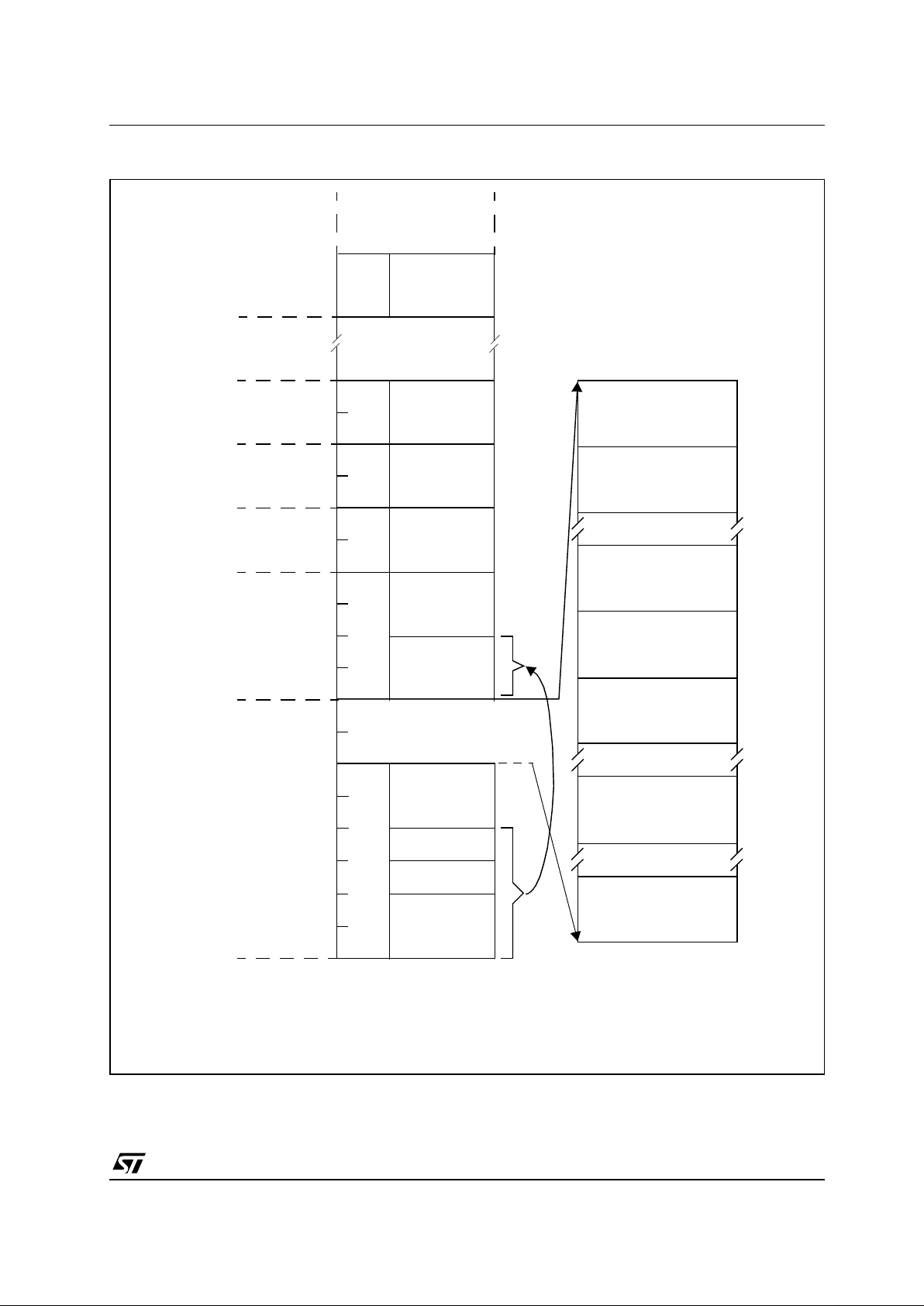
Figure 4 : ST10F280 On-chip Memo ry Mapping
14
07
06
05
04
00’4000
01
00
00’0000
02
00’C000
00’FFFF
SFR : 512 Bytes
00’FE00
00’FDFF
IRAM : 2K Bytes
00’F600
* Blocks 0, 1 and 2 may be remapped from segment 0 to segment 1 by setting SYSCON-ROMS1 (before EINIT)
RAM, SFR and X-pheripherals are
mapped into the address space.
Segment 4Segment 3Segment 2Segment 1Segment 0
Data
Page
Number
Absolute
Memory
Address
00’6000
00’F1FF
ESFR : 512 Bytes
00’F000
00’EFFF
CAN1 : 256 Byte s
00’EF00
00’EEFF
CAN2 : 256 Byte s
00’EE00
00’C3FF
XPORT9 XTIMER
00’C000
03
00’ECFF
XPWM
00’EC00
Block2 = 8K Bytes
Internal
Flash
Memory
Block1 = 8K Bytes
Block0 = 16K Bytes
01’0000
01’8000
02’0000
03’0000
0C
04’0000
10
05’0000
Block6 = 64K Bytes
Block5 = 64K Bytes
Block4 = 64K Bytes
Block3 = 32K Bytes
Block2*
Block1*
Block0*
Data Page Number and A bsolute Memory Address are hexadecim al values.
08
08’0000
20
Block10 = 64K Bytes
Segment 8
09’0000
00’8000
00’BFFF
XRAM = 16K Bytes
XPORT10
XADCMUX

ST10F280
20/186
XPERCON (F024h / 12h) ESFR Reset Value: - - 05h
Note: - When both CAN and XPWM are disabled via XPERCON setting, then any access in the address
range 00’EC00h 00’EF FFh will be directed to external mem ory interface, using the BUSCONx
register corresponding to address matching ADDRSELx register. P4.4 and P4.7 can be used as
General Purpo se I/O when CAN2 is no t enabled, and P4.5 and P4. 6 can be used as G eneral
Purpose I/O when CAN1 is not enabled.
- The default XPER selection after Reset is : XCAN1 is enabled, XCAN2 is disabled, XRAM is
enabled, XPORT9, XTIMER, XPORT10, XPWM, XADCMUX are disabled.
- Register XPERCON cannot be changed after the global enabling of XPeripherals, i.e. after
setting of bit XPEN in SYSCON register.
15141312111098765 4 3 2 1 0
-----------XPWMENXPERCONEN3XRAMENCAN2ENCAN1EN
RW RW RW RW RW
Bit Function
CAN1EN
0
1
CAN1 Enable Bit
Accesses to the on- chip CAN 1 XPeripheral a nd its fu nctions are disabled. P4.5 a nd P4.6 pins
can be used as gen eral purpose I/Os. Addre ss range 00’EF00h-00’EF FFh is only directed to
external memory if CAN2EN and XPWM bits are cleared also.
The on-chip CAN1 XPeripheral is enabled and can be accessed.
CAN2EN
0
1
CAN2 Enable Bit
Accesses to the on- chip CAN 2 XPeripheral a nd its fu nctions are disabled. P4.4 a nd P4.7 pins
can be us ed as gene ral purpos e I/Os. Addres s range 00’E E00h-00’EEFFh is only di rected to
external memory if CAN1EN and XPWM bits are cleared also.
The on-chip CAN2 XPeripheral is enabled and can be accessed.
XRAMEN
0
1
XRAM Enable Bit
Accesses to the on-chip 16K Byte XRAM are disabled, external access performed.
The on-chip 16K Byte XRAM is enabled and can be accessed.
XPERCONEN3
0
1
XPORT9, XTIMER, XPORT10, XADCMUX Enable Bit
Accesses to the XPORT9, XTIMER, X PORT10, XADCMUX p eripherals are d isabled, external
access performed.
The on-chip XPORT9, XTIMER, XPORT10, XADCMUX peripherals are enabled and can be
accessed.
XPWMEN
0
1
XPWM Enable Bit
Accesses to the on-chip XPWM are disabled, external access performed. Address range
00’EC00h-00’ECFFh is only directed to external memory if CAN1EN and CAN2EN are ‘0’ also
The on-chip XPWM is enabled and can be accessed.

ST10F280
21/186
5 - INTERNAL FLASH MEMORY
5.1 - Overview
– 512K Byte on-chip Flash memory
– Two possibilities of Flash mapping into the CPU
address space
– Flash memory can be used for code and data
storage
– 32-bit, zero waitstate read ac cess (50ns cycle
time at f
CPU
= 40MHz)
– Erase-Program Controller (EPC) similar to
M29F400B STM’s stand-alone Flash memo ry
• Word-by-Word Programmable (16µs t ypic a l)
• Data polling and Toggle Protocol for EPC
Status
• Internal Power-On detection circuit
– Memory Erase in blocks
• One 16K Byte, two 8K Byte, one 32K Byte,
seven 64K Byte blocks
• Each block can be erased separately
(1.5 second typical)
• Chip erase (8.5 second typical)
• Each block can be separately protected
against programming and erasing
• Each protected block can be temporary unprotected
• When enabled, the read protection prevents
access to data in Flash memory using a program running out of the Flash memory space.
Access to data of internal Flash can only be performed with an inner protected program
– Erase Suspend and Res um e Modes
• Read and Program another Block during erase
suspend
– Single Voltage operat ion , no need of dedicat ed
supply pin
– Low Power Consumption:
• 45mA max. Read current
• 60mA max. Program or Erase current
• Automatic Stand-by-mode (50µA maximum)
– 100,000 Erase-Program Cycles per block,
20 y ea r data reten tion time
– Operating tempe rature: -40 to +125
o
C
5.2 - Operational Overview
Read M ode
In standard mode (the normal operating mode)
the Flash ap pears like an on-chip ROM with the
same timing and functiona lity. The Flash modul e
offers a fast access time, allowing zero waitstate
access with CPU frequency up to 40MHz.
Instruction fetches and data operand reads are
performed with all addressing modes of the
ST10F280 instruction set.
In order to optimize the programming tim e of the
internal Flash, blocks of 8K Bytes, 16K Bytes,
32K Bytes, 64K Bytes can be used. But the size of
the blocks does not apply to the whole memory
space, see details in Table 2.
Table 2 : 512K Byte Flash Memory Block Organisation
Block Addresses (Segment 0) Addresses (Segment 1) Size (K Byte)
0
1
2
3
4
5
6
7
8
9
10
00’0000h to 00’3FFFh
00’4000h to 00’5FFFh
00’6000h to 00’7FFFh
01’8000h to 01’FFFFh
02’0000h to 02’FFFFh
03’0000h to 03’FFFFh
04’0000h to 04’FFFFh
05’0000h to 05’FFFFh
06’0000h to 06’FFFFh
07’0000h to 07’FFFFh
08’0000h to 08’FFFFh
01’0000h to 01’3FFFh
01’4000h to 01’5FFFh
01’6000h to 01’7FFFh
01’8000h to 01’FFFFh
02’0000h to 02’FFFFh
03’0000h to 03’FFFFh
04’0000h to 04’FFFFh
05’0000h to 05’FFFFh
06’0000h to 06’FFFFh
07’0000h to 07’FFFFh
08’0000h to 08’FFFFh
16
8
8
32
64
64
64
64
64
64
64

ST10F280
22/186
Instructions and Commands
All operations besides normal read operations are
initiated and controlled by command sequences
wri tte n to the Fla sh C om ma n d I nter fac e ( CI) . T h e
Command Interface (CI) interprets words written
to the Flash memory and enables one of the
following operations:
– Read memory array
– Program Word
– Block Erase
– Chip Erase
– Erase Suspend
– Erase Resume
– Block Protection
– Block Temporary Unprotection
– Code Protection
Commands are composed o f several write cycles
at specific addresses of the Flash memory. The
different write cycles of such command
sequences offer a fail-safe feature to protect
against an inadvertent write.
A command only starts when the Command
Interface has decoded the last write cycle of an
operation. Until that last write is performed, Flas h
memory rema ins in Read Mo de
Notes: 1. As it is not possible to perform write
operations in the Flash while fetching code
from Flash, the Flash commands must be
written by instructions executed from
internal RAM or ex ternal memo ry.
2. Command write c ycles do not need to
be consecutively received, pauses are
allowed, save for Block Erase command.
During this operation all Erase Confirm
commands mus t be sent to co mplete any
block erase operation before time-out
period expires (typically 96µs). Command
sequencing must be followed exactly. Any
invalid combination of commands will reset
the Command Interface to Read Mode.
Status R egister
This register is used to flag the status of the
memory and the result of an operation. This
register can be accessed by read cycles during
the Erase-Program Controller (EPC) operation.
Erase Operation
This Flash memory features a block erase
architecture with a chip erase capabi lity too. Erase
is accomplished by exec uting the six cycle erase
command sequence. Additional command write
cycles can then be performed to erase more than
one block in parallel . When a time-out period elaps
(96
µ
s) after the last cycle, the Erase-Program
Controller (EPC) automatically starts and times the
erase pulse and executes the erase operation.
There is no need to program the block to be
erased with ‘0000h’ before an erase operation.
Term ination of operation is indicated in the Flash
status register. After erase operation, the Flash
memory locations are read as 'FFFFh’ value.
Erase Suspend
A block erase operation is typically executed
within 1.5 second for a 64K Byte block. Erasure of
a memory block may be suspended, in order to
read data from another block or to program data in
another block, and then resumed.
In-System Programming
In-system programming is fully supported. No
special programming voltage is required. Because
of the automatic execution of erase and
programming algorithms, write operations are
reduced to transferring commands and data to the
Flash and reading the status. Any code that
programs or erases Flash memory lo cations (that
writes data to the Flash) must be executed from
memory out side the on-chip Flash memory its elf
(on-chip RAM or external memory).
A boot mechanism is provided to support
in-system programming. It wor ks using seria l link
via USART interface and a PC compatible or
other programming host.
Read/Write Protection
The Flash module supports read and write
protection in a very comfortable and advanced
protection functionality. If Read Protection is
installed, the whole Flash memory is protected
against any "external" read access; read
accesses are only possible with instructions
fetched directly from program Flash memory. For
update of the Flas h memor y a temporar y disable
of Flash Read Protection is supported.
The device also features a block write protection.
Software locking of selectable memory blocks is
provided to protect code and data. This feature
will disable both program and erase operations in
the selected block(s) of the memory. Block
Protection is accomplished by block specific
lock-bit which are programmed by executing a
four cycle command sequence. The locked state
of blocks is indicated by specific flags in the
according block status registers. A block may only
be temporarily unlocked for update (write)
operations.

ST10F280
23/186
With the two possibilities for write protection whole
memory or block specific a flexible installation of
write protection is suppor ted to protect the Flash
memory or parts of it from unauthorized
programming or erase accesses and to provide
virus-proof protection for all system code blocks.
All write protection also is enabled during boot
operation.
Power Supply, Reset
The Flash modul e uses a si ngle power supply for
both read and write functions. Internally generated and regulated voltages are provided for the
program and erase operations from 5V supply.
Once a program or erase cycle has been completed, the device resets to the standard read
mode. At power-on, the Flash memory has a
setup phase of some microseconds (dependent
on the power supply ramp-up). During this phase,
Flash can not be read. Thus, if EA
pin is high (execution will start from F lash m em or y ), the CP U will
remains in reset state until the Flash can be
accessed.
5.3 - Architectural Description
The Flash module distinguishes two basic
operating modes, the standard read mode and the
command mo de. The initial state after power-on
and after reset is the standard read mode.
5.3.1 - Read Mode
The Flash modul e enters the standard operating
mode, the read mode:
– After Reset command
– After every completed erase operation
– After every completed programming operation
– After every other completed command
execution
– Few microseconds after a CPU-reset has
started
– After incorrect address and data values of
command sequences or writing them in an
improper sequence
– After incorrect write access to a read protected
Flash memory
The read mode remains active until the last
command of a command sequence is decoded
which starts directly a Flash array operation, such
as:
– erase one or several blocks
– program a word into Flash array
– protect / temporary unprotect a block.
In the standard read mode read accesses are
directly controlled by the Flash memory array,
delivering a 32-bit double Word from the
addressed position. Read accesses are always
aligned to double Word boundaries. Thus, both
low order address bit A1 and A 0 are not used in
the Flash array for read accesses. The high order
address bit A18/A17/A16 define the physical
64K Bytes segment being accessed within the
Flash array.
5.3.2 - Command Mode
Every operation besides standard read operations
is initiated by commands written to the Flash
command register. The addresses used for
command cycles define in conjunction with the
actual state the specific step within command
sequences. With the last command of a command
sequence, the Erase-Program Controller (EPC)
starts the execution of the command. The EPC
status is indicated during comman d execution by:
– The Status Register,
– The Ready/Bu sy signal.
5.3.3 - Flash Status Register
The Flash Status register is used to flag the status
of the Flash memory and the result of an
operation. This register can be accessed by Read
cycles during the program-Erase Controller
operations. The program or erase operation can
be controlled by data polling on bit FSB.7 of
Status Register, detection of Toggle on FSB.6 and
FSB.2, or Error on FSB.5 and Erase Timeout on
FSB.3 bit. Any read attempt i n Flash during E PC
operation will a utomatic ally ou tput thes e five bits.
The EPC sets bit FSB.2, FSB.3, FSB.5, FSB.6
and FSB.7. Other bit are reserved for future use
and should be masked.

ST10F280
24/186
Flash Status (see note for address)
Note: The Address of Flash Status Register is the address of the word being programmed when
Programming operation is in progress, or an address w ithin block being erased when Erasing
operation is in progress.
15 14 13 12 11 10 9 8 7 6 5 4 3 2 1 0
-------- FSB.7 FSB.6 FSB.5 - FSB.3 FSB.2 - RRR R R
FSB.7 Flash Status bit 7: Data Polling Bit
Programming Operation: this bit outputs the complement of the bit 7 of the word being
programm ed , and after com ple t ion , w ill ou t pu t the b it 7 of the wo rd progr ammed.
Erasing Operation: outputs a ‘0’ during erasing, and ‘1’ after erasing completion.
If the block selected f or erasure is (are) protected, FSB.7 will be set to ‘0’ for about 100 µs, and
then return to the previous addressed memory data value.
FSB.7 will also flag t he Erase Suspend Mode by switching from ‘0’ to ‘1’ at the star t of the
Erase Suspend.
During Program operation in Erase Suspend Mode, FSB.7 will have the same behaviour as in
normal Program execution outside the Suspend mode.
FSB.6 Fl ash S t at us bit 6: Toggle Bit
Programming or Erasing Operations: successive read operations of Flash Status register will
deliver complementary values. FSB.6 will togg le each time the Flash Status register is read.
The Program operation is completed wh en two successive reads yield the same value. The
next read will output the bit last programmed, or a ‘1’ after Erase operation
FSB.6 will be set to‘1’ if a read operation is attempted on an Erase Suspended block. In
addition, an Erase Suspend/Resume command will cause FSB.6 to toggle.
FSB.5 Flash Status bit 5: Error Bit
This bit is set to ‘1’ when there is a failure of Program, block or chip erase operations.This bit
will also be set if a user tries to program a bit to ‘1’ to a Flash location that is currently
programmed with ‘0’.
The error bit resets after Read/Reset instruction.
In case of success, the Error bit w il l be set to ‘0’ during Program or Erase and then w ill o utpu t
the bit last programmed or a ‘1’ after erasing
FSB.3 Flash Status bit 3: Erase Time-out Bit
This bit is cleared by the EPC when the las t Block Erase command has been en tered to the
Command Interface and it is awaiting the Erase start. When the time-out period is finished,
after 96 µs, FSB.3 returns back to ‘1’.
FSB.2 Fl ash S t at us bit 2: Toggle Bit
This toggle bit, together with FSB.6, can be used to determine the chip status during the Erase
Mode or Erase Suspend Mode. It can be used also to identify the block being Erased
Suspended. A Read operation will cause FS B.2 to Toggle during the Erase Mode. If the Flash
is in Erase Suspend Mode, a Read operation from the Erase suspen ded block or a Program
operation into the Erase suspended block will cause FSB.2 to toggle.
When the Flash is in Program Mode during Erase Suspend, FSB.2 will be read as ‘1’ if address
used is the address of the word being programmed.
After Erase completion with an Error status, FSB.2 will toggle when reading the faulty sector.

ST10F280
25/186
5.3.4 - Flash Protection Register
The Flash Protection register is a non-volatile register that contains the protection status. This register
can be read by using the Read Protection St atus (RP) command, and programmed by using the de dicated Set Protection command.
Flash Protection Register (PR)
5.3.5 - Instructions Description
Twelve instructions dedicated to Flash memory
accesses are defined as follow:
Read/Reset (RD). The Read/Reset instruction
consist of one write cycle with data XXF0h . it can
be optionally preceded by two CI enable
coded
cycles (data xxA8h at address 1554h + data
xx54h at address 2AA8h). Any successive read
cycle following a Read/Reset instruction will read
the memory array. A Wait cycle of 10µs is
necessary after a Read/Reset command if the
memory was in program or Erase mode.
Program Word (PW). This instruction uses four
write cycles. After the two Cl enable coded cycles ,
the Program Word command xxA 0h is written at
address 1554h. The following write cycle will latch
the address and data of the word to be
programmed. Memor y p rogramming can be do ne
only by writing 0's instead of 1's, otherwise an
error occurs. During programming, the Flash
Status is checked by reading the Flash Status bit
FSB.2, FSB.5, FSB.6 and FSB.7 which show the
status of the EPC. FSB.2, FSB.6 and FSB.7
determine if programming is on going or has
completed, and FSB.5 allows a check to be made
for any possible error .
Block Erase (BE). This instruction uses a
minimum of six command cycles. The erase
enable command xx80h is written at address
1554h after the two-cycle CI enable sequence.
The erase confirm code xx30h must be written at
an address related to the block to be erased
preceded by the execution of a second CI enable
sequence. Additional erase confirm codes must
be given to erase m ore than on e block in parallel.
Additional erase confirm commands must be
written within a defined time-ou t perio d. The input
of a new Block Erase command will restart the
time -out period.
When this time-out period has elapsed, the erase
starts. The status of the internal timer can be
monitored through the level of FSB.3, if FSB.3 is
‘0’, the Block Erase command has been given and
the timeout is running ; if FSB.3 is ‘1’, the timeout
has expired and the EPC is erasing the block(s).
If the second command given is not an erase confirm or if the coded cycles are wrong, the instruction aborts, and the device is reset to Read Mode.
1514131211109876543 210
CP ----BP10 BP9 BP8 BP7 BP6 BP5 BP4 BP3 BP2 BP1 BP0
RW RW RW RW RW RW RW RW RW RW RW RW
BPx Block x Protection bit (x = 0...10)
‘0’: the Block Protection is enabled for block x. Programming or erasing the block is not
possible, unless a Block Temporary Unprotection command is issued.
1’: the Block Protection is disabled for block x.
Bit is ‘1’ by default, and can be programmed permanently to ‘0’ using the Set Protection
command but then cannot be set to ‘1’ again. It is therefore possible to temporally disable the
Block Protection using the Block Temporary Unprotection instruction.
CP Code Protection Bit
‘0’: the Flash Code Protection is enabled. Read accesses to the Flash for execution not
performed in the Flash itself are not allowed, the returned value will be 009Bh, whatever the
content of the Flash is.
1’: the Flash Code Protection is disabled: read accesses to the Flash from external or internal
RAM are allowed
Bit is ‘1’ by default, and can be programmed permanently to ‘0’ using the Set Protection
command but then cannot be set to ‘1’ again. It is therefore possible to temporarily disable the
Code Protection using the Code Temporary Unprotection instruction.

ST10F280
26/186
It is not necessary to program the block with
0000h as the EPC will do this automatically before
the erasing to FFFFh. Read operations after the
EPC has sta rted, output the Flash Status Register. During the execution of the erase by the EPC,
the device accepts only the Erase Suspend a nd
Read/Reset instructions. Data Polling bit FSB.7
returns ‘0’ while the erasure is in progress, and ‘1’
when it has completed. The To ggle bit FSB.2 and
FSB.6 toggle during the erase operation. They
stop when erase is completed. After completion,
the Error bit FSB.5 returns ‘1’ if there has been an
erase failure because erasure has not comp leted
even after the maximum number of erase cycles
have been executed by the EPC, in this case, it
will be necessary to input a Read/Reset to the
Command Interface in order to reset the EPC.
Chip Erase (CE). This instruction uses six write
cycles. The Erase Enable command xx80h, must
be written at address 1554h after CI-Enable
cycles. The Chip Erase command xx10h must be
given on the sixth cycle after a second C I-Enable
sequence. An error in command sequence will
reset the CI to Read mode. It is NOT necessary to
program the block with 0000h as the E PC will do
this automatically before the erasing to FFFFh.
Read operations after the EPC has star ted out put
the Flash Status Register. During the execution of
the erase by the EPC, Data Polling bit FSB.7
returns ‘0’ while the erasure is in progress, and ‘1’
when it has completed. The FSB.2 and FSB.6 bit
toggle during the erase operation. They stop when
erase is finished. The FSB.5 error bit returns "1" in
case of failure of the erase operation. The error
flag is set after the maximum number of erase
cycles have been executed by the EPC. In this
case, it will be necessary to input a Read/Reset to
the Command Interface in order to reset the EPC.
Erase Suspend (ES). This instruction can be
used to suspend a Block Erase operation by
giving the command xxB0h without any specific
address. No CI-Enable cycles is required. Erase
Suspend operation allows reading of data from
another block and/or the programming in another
block while erase is in progress. If this com mand
is given during the time-out period, it will terminate
the time-out period in addition to erase Suspend.
The Toggle Bit FSB.6, when monitored at an
address that belongs to the block being erased,
stops toggling when Erase Suspend Command is
effective, It happens between 0.1µs and 15µs
after the Erase Suspend Command has been
written. The Flash will then go in normal Read
Mode, and read from blocks not being erased is
valid, while read from block being erased will
output FSB.2 toggling. Dur ing a Suspend phase
the only instructions valid are Erase Resum e and
Program Word. A Read / Reset instruction d uring
Erase suspend wi ll definitely abor t th e Erase a nd
result in invalid data in the block being erased.
Erase Resume (ER). This instruction can be
given when the memory is in Erase Suspend
State. Erase can be resumed by writing the
command xx30h at any address without any
Cl-enable sequence.
Program during Erase Sus pend. The Program
Word instruction during Erase Suspend is allowed
only on blocks that are not Erase-suspended. This
instruction is the same than the Program Word
instruction.
Set Prote c t io n (SP). This instruction can be used
to enable both Block Protection (t o protect each
block independently from accidental Erasing-Programming Operation) and Code Protection (to
avoid code dump). The Set Protection Com mand
must be given after a s pecial CI-Prot ection Enab le
cycles (see instruction table). The following Write
cycle, will p rogr am the Prote cti on Register. T o pro tect the block x (x = 0 to 10), the data bit x must be
at ‘0’. To protect the code, bit 15 of the data must
be ‘0’. Enabling Block or Code Protecti on is per-
manent and can be cleared only by STM. Block
Temporary Unprotection and Code Temporary
Unprotection instructions are available to allow the
customer to update the code.
Note: 1. The new value programmed in
protect ion regis ter will onl y becom e active
after a reset.
2. Bit that are already at ’0’ in protec tion
register must be confirmed at ’0’ also in
data latched during the 4th cycle of set
protection command, otherwise an error
may occur.
Read Protection Status (RP). This instru ction is
used to read the Block Protection status and the
Code Protection status. To read the protection
register (see Table 3), the CI-Protection Enable
cycles must be executed followed by the
command xx90h at address x2A54h. The
following Read Cycles at any odd word address
will output the Block Protection Status. The Read/
Reset command xxF0h must be written to reset
the protection interface.
Note: After a modification of protection register
(using Set Protection command), the Read
Protection Status will return the new PR
value only after a reset.

ST10F280
27/186
Block Temporary Unprotection (BTU). This Instruction can be used to temporar y unprotect all the
blocks from Program / Erase protection. The Unprotection is disabled after a Reset cycle. The Block
Tem porary Unprotection command xxC1h must be given to enable Block Temporar y Unprotection. The
Command must be preceded by the CI-Protection Enable cycles and followed by the Read/Reset
command xxF0h.
Set Code Protection (SCP). This kind of protection allows the customer to protect the proprietar y code
written in Flash. If installed and active, Flash Code Protection prevents data operand accesses and
program branches into the on-chip Flash area from any location outside the Flash memory itself. Data
operand accesses and branches to Flash locations are only and exclusively allowed for instructions
executed from the Flash memory itself. Every read or jump to Flash performed from another memory (like
internal RAM, external me mory) while Code Protection is enabled, will give the opcode 009Bh related to
TRAP #00 illegal instruction. The CI-Protection Enable cycles must be sent to set the Code Protection. By
writing data 7FFFh at any odd word addre ss, the Code Protec ted status is stored in the Flash Pr otec tion
Register (PR). Protection is permanent and cannot be cleared by the user. It is possible to temporarily
disable the Code Protection using Code Te mpo rar y Unprot ection instr uc tion.
Note: Bits that are already at ’0’ in protection register must be confirmed at ’0’ also in data latched during
the 4th cycle of set protection command, otherwise an error may occur.
Code Temporary Unprotection (CTU). This instruction must be used to temporary disable Code
Protection. This instruction is effective only if executed from Flash memory space. To restore the
protection status, without using a reset, it i s necessar y to use a Code Temporary Protection instruction.
System reset will reset also the Code Tem porary Unprotected status. The Code Temporary Unprotection
command consists of the following write cycle:
MOV MEM, Rn ; This instruction MUST be executed from Flash memory space
Where MEM is an absolute address inside memor y space, Rn is a register loaded with data 0FFFFh.
Code Temporary Protection ( C TP). This instruction allows to restore Code Protection. This operation is
effective only if executed from Flash memory and is necessar y to restore the protection status after the
use of a Code Temporary Unprotection instruction.
The Code Tem porary Protection command consist s of the following write cycle:
MOV MEM, Rn ; This instruction MUST be executed from Flash memory space
Where MEM is an absolute address inside memor y space, Rn is a register loaded with data 0FFFBh.
Note that Code Temporary Unprotection instruc tion must be used when it is necessary to modify the
Flash with protected code (SCP), since the write/erase routines must be executed from a memory
external to Flash space. Usually, the write/erase routines, executed in RAM, ends w ith a retur n to Flash
space where a CTP instruction restore the protection.
ST10F280
28/186
Table 3 : Instructions
Notes 1. Address bit A14, A15 and above are don’t care for coded add ress inputs.
2. X = Don’t Care.
3. WA = Write Address: addre ss of memory l ocation to be programmed.
4. WD = Write D ata: 16-bit data to be programmed
5. Optional , additi onal blocks addresses m ust be entered wi thin a ti m e-out delay (96 µs) after la st write entry, timeout st atus can be
verified th rough FSB.3 valu e. W hen full command is entered, read Dat a Poll i ng or Toggle bit unt i l Erase is compl et ed or suspended.
6. Read Data Polling or Tog gle bit until Erase completes.
7. WPR = W rite pro t ection regi ster. To protect code, bit 15 of WPR m ust be ‘0’. To protect blo ck N (N=0,1,.. .), bit N o f WPR must be
‘0’. Bit that are already at ‘0’ in protection register must also be ‘0’ in WPR, else a writing error will occurs (it is not possible to write a
‘1’ in a bit already programmed at ‘0’).
8. MEM = any add ress insid e the Fl ash m emor y s pace. Absolu te add ress ing m ode m ust be used (M OV MEM, Rn) , and ins tru cti on
must be executed from F l ash memory space.
9. Odd word address = 4n-2 w here n = 0, 1, 2, 3..., ex. 0002h, 0006h. ..
Instruction Mne Cycle
1
st
Cycle
2
nd
Cycle
3rd
Cycle
4th Cycle
5th
Cycle
6th
Cycle
7th
Cycle
Read/Reset RD 1+
Addr.
1
X
2
Read Memory Array until a new write cycle is initiated
Data xxF0h
Read/Reset RD 3+
Addr.
1
x1554h x2AA8h xxxxxh
Read Memory Array until a new write
cycle is initiated
Data xxA8h xx54h xxF0h
Program Word PW 4
Addr.
1
x1554h x2AA8h x1554h WA
3
Read Data Polling or
Toggle Bit until Program
completes.
Data xxA8h xx54h xxA0h WD
4
Block Erase BE 6
Addr.
1
x1554h x2AA8h x1554h x1554h x2AA8h BA BA’
5
Data xxA8h xx54h xx80h xxA8h xx54h xx30h xx30h
Chip Erase CE 6
Addr.
1
x1554h x2AA8h x1554h x1554h x2AA8h x1554h
Note
6
Data xxA8h xx54h xx80h xxA8h xx54h xx10h
Erase Suspend ES 1
Addr.
1
X
2
Read until Toggle stops, then read or program all data needed
from block(s) not being erased then Resume Erase.
Data xxB0h
Erase Resume ER 1
Addr.
1
X
2
Read Data Polling or Toggle bit until Erase completes or Erase
is supended another time.
Data xx30h
Set Block/Code
Protection
SP 4
Addr.
1
x2A54h x15A8h x2A54h Any odd
word
address
9
Data xxA8h xx54h xxC0h WPR
7
Read
Protection
Status
RP 4
Addr.
1
x2A54h x15A8h x2A54h Any odd
word
address
9
Read Protection Register
until a new write cycle is
initiated.
Data xxA8h xx54h xx90h Read
PR
Block
Temporary
Unprotection
BTU 4
Addr.
1
x2A54h x15A8h x2A54h X
2
Data xxA8h xx54h xxC1h xxF0h
Code
Temporary
Unprotection
CTU 1
Addr.
1
MEM
8
Write cycles must be executed from Flash.
Data FFFFh
Code
Temporary
Protection
CTP 1
Addr.
1
MEM
8
Write cycles must be executed from Flash.
Data FFFBh

ST10F280
29/186
– Generally, command sequences cannot be
written to Flash by instructions fetched from the
Flash itself. Thus, the Flash commands must be
written by instructions, executed from internal
RAM or external memory.
– Command cycles on the CPU interface need not
to be consecutively recei ved (pauses allowed).
The CPU interface delivers dummy read data for
not used cycles within command sequences.
– All addresses of command cycles shall be
defined only with Register-indirect addressing
mode in the according move instructi o ns. Di re ct
addressing is not allowed for command
sequences. Address segment or data page
pointer are taken into account for the com mand
address value.
5.3.6 - Reset Processing and Initial State
The Flash module distinguishes two kinds of CPU
reset types
The lengthening of CPU reset:
– Is not reported to external devices by
bidirectional pin
– Is not enabled in case of external start of CPU
after reset.
5.4 - Flash Memory Configuration
The default memory configuration of the
ST10F280 Memor y is determined by the state of
the EA
pin at reset. This value is stored in the
Internal ROM Enable bit (named ROMEN) of the
SYSCON register.
When ROMEN = 0, the interna l Flash is disabled
and external ROM is used for startup control.
Flash memor y can la ter be enabled by setting the
ROMEN bit of SYSCON to 1. The code
performing this setting must not run from a
segment of the extern al ROM to be replaced by a
segment of the Flash memory, otherwise
unexpected behaviour may occur.
For example, if external ROM code is located in
the first 32K Bytes of segment 0, the first
32K Bytes of the Flash must then be enabled in
segment 1. This is done by setting the ROMS1 bit
of SYSCON to 0 before or simultaneously with
setting of ROMEN bit. This must be done in the
externally supplied program before the execution
of th e EINI T inst ruction.
If program execution starts from external memory,
but access to the Flash memory mapped in
segment 0 is later required, then the code that
performs the setting of ROMEN bit must be
executed either in the segment 0 but above
address 00’8000h, or from the internal RAM.
Bit ROMS1 only affects the mapping of the first
32K Bytes of t he Flash memor y. All other par t s of
the Flash memory (addresses 01’8000h
08’FFFFh) remain unaffected.
The SGTDIS Segmentation Disable / Enable must
also be set to 0 to allow the use of the full
512K Bytes of on-c hip memory i n addition to the
external boot memor y. The correct procedure on
changing the segmentation registers must also be
observed to prevent an unwanted trap condition:
– Instructions that configure the internal mem ory
must only be executed from external memory or
from the internal RAM.
– An Absolute Inter-Segment Jump (JMPS)
instruction must be executed after Flash
enabling, to the next instruction, even if this next
instruction is located in the consecutive address.
– Whenever the internal Memory is disabled,
enabled or remapped, the DPPs must be
explicitly (re)loaded to enable correct data
accesses to the internal memory and/or external
memory.
5.5 - Application Examples
5.5.1 - Handling of Flash Addresses
All command, Block, Data and register addresses
to the Flash have to be located w ithin the active
Flash memory space. The active space is that
address range to which the physical Flash
addresses are mapped as defined by the user.
When using data page pointer (DPP) for block
addresses make sure that address bit A15 and
A14 of the block address are reflected in both
LSBs of the selected DPPS.
Note: - For Command Instructions, address bit
A14, A15, A16, A17 and A18 are don’t
care. This simplify a lot the application
software, because it minimize the use of
DPP registers when using Command in
the Command Interface.
- Direct addressing is not allowed for
Command sequence operations to the
Flash. Only Register-indirect addressing
can be used for command, block or
write-data accesses.

ST10F280
30/186
5.5.2 - Basic Flash Access Control
When accessing the Flash all command write addresses have to be located within the active Flash
memory s pace. The active Flash memor y space is that logical address range which is covered by the
Flash after mapping. When using data page pointer (DPP) for addressing the Flash, make sure that
address bit A15 and A14 of the command addresses are reflected in both LSBs of the selected data page
pointer (A15 DPPx.1 and A14 DPPx.0).
In case of the command write addresses, address bit A14, A15 and above are don’t care. Thus, command
writes can be performed by only using one DPP register. This allow to have a more simple and com pact
application software.
Another advantageous possibility is to use the extended segment instruction for addressing.
Note: The direct addressing mode is not allowed for write access to the Flash address/command
register. Be aware that the C compiler may use this kind of addressing. For write accesses to
Flash module always the indirect addressing mode has to be selected.
The following basic instruction sequences show examples for different addressing possibilities.
Principle example of address generation for Flash commands and registers:
When using data page pointer (DPP0 is this example)
MOV DPP0,#08h ;adjust data page pointers according to the
;addresses: DPP0 is used in this example, thus
;ADDRESS must have A14 and A15 bit set to ‘0’.
MOV Rw
m
,#ADDRESS ;ADDRESS could be a dedicated command sequence
;address 2AA8h, 1554h ... ) or the Flash write
;address
MOV Rw
n
,#DATA ;DATA could be a dedicated command sequence data
;(xxA0h,xx80h ... ) or data to be programmed
MOV [Rw
m
],Rw
n
;indirect addressing
When using the extended segment instruction:
MOV Rw
m
,#ADDRESS ;ADDRESS could be a dedicated command sequence
;address (2AA8h, 1554h ... ) or the Flash write
;address
MOV Rw
o
,#DATA ;DATA could be a dedicated command sequence data
;(xxA0h,xx80h ... ) or data to be programmed
MOV Rw
n
,#SEGMENT ;the value of SEGMENT represents the segment
;number and could be 0, 1, 2, 3 or 4 (depending
;on sector mapping) for 256KByte Flash.
EXTS Rw
n
,#LENGTH ;the value of Rwn determines the 8-bit segment
;valid for the corresponding data access for any
;long or indirect address in the following(s)
;instruction(s). LENGTH defines the number of
;the effected instruction(s) and has to be a value
;between 1...4
MOV [Rw
m
],Rw
o
;indirect addressing with segment number from
;EXTS

ST10F280
31/186
5.5.3 - Programming Examples
Most of the microcont roller programs are written in the C language wh ere the data page pointers are
automatically set by the compiler. But because the C compiler may use the not allowed direct addressing
mode for Flash write addresses, it is necessary to program the organisational Flash accesses (command
sequences) with assembler in-line routines which use indirect addressing.
Example 1 Performing the command Read/Reset
We assume that in the initialization phase the lowest 32K Bytes of Flash memor y (sector 0) have been
mapped to segment 1.
According to the usual way of ST10 data addressing with data page pointers, address bit A15 and A14 of
a 16-bit command write addres s select the data page pointer (DPP) w hich contain s the upp er 10-bit for
building the 24-bit physical data address. Address bit A13...A0 represent the addres s offset. As the bit
A14...A18 are "don’t care" when written a Flash command in the Command Interface (CI), we can choose
the most conveniant DPPx register for address handling.
The following examples are making usage of DPP0. We just have to make sure, that DPP0 points to
active Flash memory space.
To be indepen dent of mapping of sector 0 we choose for all DPPs which are used for Flash address
handling, to point to segment 2.
For this reason we load DPP0 with value 08h (00 0000 l000b).
MOV R5, #01554h ;load auxilary register R5 with command address
;(used in command cycle 1)
MOV R6, #02AA8h ;load auxilary register R6 with command address
;(used in command cycle 2)
SCXT DPPO, #08h ;push data page pointer 0 and load it to point to
;segment 2
MOV R7, #0A8h ;load register R7 with 1st CI enable command
MOV [R5], R7 ;command cycle 1
MOV R7, #054h ;load register R7 with 2cd CI enable command
MOV [R6], R7 ;command cycle 2
MOV R7, #0F0h ;load register R7 with Read/Reset command
MOV [R5], R7 ;command cycle 3. Address is don’t care
POP DPP0 ;restore DPP0 value
In the example above the 16-bit registers R5 and R6 are used as auxilary registers for indirect
addressing.
Example 2 Performing a Program Word command
We assume that in the initialization phase the lowest 32K Bytes of Flash memor y (sector 0) have been
mapped to segme nt 1.Th e data to be wri tten is lo aded i n registe r R13, the a ddress to be programmed is
loaded in register R11/R12 (segment number in R11, segment offset in R12).
MOV R5, #01554h ;load auxilary register R5 with command address
;(used in command cycle 1)
MOV R6, #02AA8h ;load auxilary register R6 with command address
;(used in command cycle 2)
SXCT DPPO, #08h ;push data page pointer 0 and load it to point to
;segment 2
MOV R7, #0A8h ;load register R7 with 1st CI enable command
MOV [R5], R7 ;command cycle 1
MOV R7, #054h ;load register R7 with 2cd CI enable command
MOV [R6], R7 ;command cycle 2
MOV R7, #0A0h ;load register R7 with Program Word command
MOV [R5], R7 ;command cycle 3

ST10F280
32/186
POP DPP0 ;restore DPP0: following addressing to the Flash
;will use EXTended instructions
;R11 contains the segment to be programmed
;R12 contains the segment offset address to be
;programmed
;R13 contains the data to be programmed
EXTS R11, #1 ;use EXTended addressing for next MOV instruction
MOV [R12], R13 ;command cycle 4: the EPC starts execution of
;Programming Command
Data_Polling:
EXTS R11, #1 ;use EXTended addressing for next MOV instruction
MOV R7, [R12] ;read Flash Status register (FSB) in R7
MOV R6, R7 ;save it in R6 register
;Check if FSB.7 = Data.7 (i.e. R7.7 = R13.7)
XOR R7, R13
JNB R7.7, Prog_OK
;Check if FSB.5 = 1 (Programming Error)
JNB R6.5, Data_Polling
;Programming Error: verify is Flash programmed
;data is OK
EXTS R11, #1 ;use EXTended addressing for next MOV instruction
MOV R7, [R12] ;read Flash Status register (FSB) in R7
;Check if FSB.7 = Data.7
XOR R7, R13
JNB R7.7, Prog_OK
;Programming failed: Flash remains in Write
;Operation.
;To go back to normal Read operations, a Read/Reset
;command
;must be performed
Prog_Error:
MOV R7, #0F0h ;load register R7 with Read/Reset command
EXTS R11, #1 ;use EXTended addressing for next MOV instruction
MOV [R12], R7 ;address is don’t care for Read/Reset command
... ;here place specific Error handling code
...
...
;When programming operation finished succesfully,
;Flash is set back automatically to normal Read Mode
Prog_OK:
....
....

ST10F280
33/186
Example 3 Performing the Block Erase command
We assume that in the initialization phase the lowest 32K Bytes of Flash memor y (sector 0) have been
mapped to segment 1.The registers R11/R12 contain an address related to the block to be erased
(segment number in R11, segment offset in R12, for example R11 = 01h, R12= 4000h will erase the block
1 first 8K byte block).
MOV R5, #01554h ;load auxilary register R5 with command address
;(used in command cycle 1)
MOV R6, #02AA8h ;load auxilary register R6 with command address
;(used in command cycle 2)
SXCT DPPO, #08h ;push data page pointer 0 and load it to point ;to
;segment 2
MOV R7, #0A8h ;load register R7 with 1st CI enable command
MOV [R5], R7 ;command cycle 1
MOV R7, #054h ;load register R7 with 2cd CI enable command
MOV [R6], R7 ;command cycle 2
MOV R7, #080h ;load register R7 with Block Erase command
MOV [R5], R7 ;command cycle 3
MOV R7, #0A8h ;load register R7 with 1st CI enable command
MOV [R5], R7 ;command cycle 4
MOV R7, #054h ;load register R7 with 2cd CI enable command
MOV [R6], R7 ;command cycle 5
POP DPP0 ;restore DPP0: following addressing to the Flash
;will use EXTended instructions
;R11 contains the segment of the block to be erased
;R12 contains the segment offset address of the
;block to be erased
MOV R7, #030h ;load register R7 with erase confirm code
EXTS R11, #1 ;use EXTended addressing for next MOV instruction
MOV [R12], R7 ;command cycle 6: the EPC starts execution of
;Erasing Command
Erase_Polling:
EXTS R11, #1 ;use EXTended addressing for next MOV instruction
MOV R7, [R12] ;read Flash Status register (FSB) in R7
;Check if FSB.7 = ‘1’ (i.e. R7.7 = ‘1’)
JB R7.7, Erase_OK
;Check if FSB.5 = 1 (Erasing Error)
JNB R7.5, Erase_Polling
;Programming failed: Flash remains in Write
;Operation.
;To go back to normal Read operations, a Read/Reset
;command
;must be performed
Erase_Error:
MOV R7, #0F0h ;load register R7 with Read/Reset command
EXTS R11, #1 ;use EXTended addressing for next MOV instruction
MOV [R12], R7 ;address is don’t care for Read/Reset command
... ;here place specific Error handling code
...
...
;When erasing operation finished succesfully,
;Flash is set back automatically to normal Read Mode
Erase_OK:
....
....

ST10F280
34/186
5.6 - Bootstrap Loader
The built-in bootstrap loader (BSL) of the
ST10F280 provides a mechanism to load the
startup program through the serial interface after
reset. In this case, no external memory or internal
Flash memory is required for the initialization
code starting at location 00’0000h (see Figure 5).
The bootstrap loader moves code/data into the
internal RAM, but can also transfer data via the
serial interface into an external RAM using a
second level loader routine. ROM Memory
(internal or external) is not necessary, but it
may be used to provide lookup tables or
“core-code” like a set of general purpose
subroutines for I/O operations, number crunching,
system initialization, etc.
The bootstrap loader can be used to load the
complete application software into ROMless
systems, to load temporary software into
complete systems for testing or calibration, or to
load a programming routine for Flash devices.
The BSL mechanism can be used for standard
system startup as well as for special occasions
like system maintenance (firmer update) or
end-of-line programming or testing.
5.6.1 - Entering the Bootstrap Loader
The ST10F280 enters BSL mode whe n pin P 0L.4
is sampled low at t he end o f a hardware reset. In
this case the built-in bootstrap loader is activated
independent of the selected bus mode.
The bootstrap loader code is stored in a special
Boot-ROM. No part of the standard mask Memory
or Flash Memory area is required for this.
After entering BSL mode and the respective
initialization the ST10F280 scans the RxD0 line to
receive a zero Byte, one start Bit, eight ‘0’ data
Bits and one stop Bit.
From the duration of this zero Byte it calculates
the corresponding Baud rate factor with respect to
the current CPU clock, initializes the serial
interface ASC0 accordingly and switches pin
TXD0 to output.
Using this Baud rate, an identification Byte is
returned to the host that provides the loaded data.
This identification Byte identifies the device to be
booted. Identification byte is D5h for the
ST10F280.
Figure 5 : Bootstrap Loader Sequence
RSTIN
TXD0
Internal Boot Memory (BSL) routine 32 Byte user software
2)
3)
RxD0
CSP:IP
4)
6)
P0L.4
1) BSL initialization time
2) Zero Byte (1 start Bit, eight ‘0’ data Bits, 1 stop Bit), sent by host.
3) Identification Byte (D5h), sent by ST10F280.
4) 32 Byte s of code / data, se nt by host.
5) Cauti on: TXD0 is onl y driven a certain tim e after rec eption of the zero Byte.
6) Internal Boot R OM .
1)
5)

ST10F280
35/186
When the ST10F280 has entered BSL mode, the following configuration is automat icall y set (values that
deviate from the normal reset values, are
marked
):
In this case, the watchdog timer is disabled, so the
bootstrap loading sequence is not time limited.
Pin TXD0 is configured as output, so the
ST10F280 can return the identification Byte.
Even if the internal Fla sh is enabled, no code can
be e xecuted out of it.
The hardware that activates the BSL duri ng reset
may be a simple p ull-down resistor on P0L.4 for
systems that use this feature upon every
hardware reset.
A switchable solution (via jumper or an external
signal) can be used for systems that
only temporarily use the bootstrap loader (see
Figure 6).
After sending the identification Byte the
ASC0 receiver is enabled and is ready to
receive the initial 32 Bytes from the host. A half
duplex connection is therefore sufficient to feed
the BSL.
5.6.2 - Memory Configuration After Reset
The configuration (and the accessibility) of the
ST10F280’s memory areas after reset in
Bootstrap-Loader mode differs from the standard
case. Pin EA
is not evaluated when BSL mode is
selected, and accesses to the interna l Flash area
are partly redirected, while the ST10F280 is in
BSL mode (see Figure 7). All code fetches are
made from the special Boot-ROM, while data
accesses read from the inter nal user Flash. Data
accesses will return undefined values on
ROMless devi ce s.
The code in the Boot-ROM is not an invariant
feature of the ST10F280. User software should
not try to execute code from the internal Flash
area while the BSL mode is still active, as these
fetches will be redirected to the B oot-ROM. The
Boot-ROM will also “move” to segment 1, when
the internal F lash area is mapped to s egment 1
(see Figure 7).
Watchdog Timer:
Disabled
Register SYSCON: 0E00h
Context Pointer CP: FA00h Register STKUN: FA40h
Stack Pointer SP: FA40h Register STKOV: FA0Ch 0<->C
Register S0CON:
8011h
Register BUSCON0: acc. to startup configuration
Register S0BG: Acc. to ‘00’ Byte
P3.10 / TXD0: ‘1’
DP3.10: ‘1’
Figure 6 : Hardware Provisions to Activate the BSL
R
POL.4
8kΩ
Circuit 1
POL.4
POL.4
Normal Boot
BSL
External
Signal
R
POL.4
8kΩ
Circuit 2

ST10F280
36/186
Figure 7 : Memory Configuration After Reset
5.6.3 - Loading the Startup Code
After sending the identification Byte the BSL
enters a loop to receive 32 Bytes via ASC0. These
Byte are stored sequentially into locations
00’FA40h through 00’FA5F h of the internal RAM.
So up to 16 instructions may be placed into the
RAM area. To execute the loaded code the BSL
then jumps to locat ion 00 ’FA40h, which is the first
loaded instruction.
The bootstrap loading sequence is now
terminated, t he ST10F280 remains in BSL mo de,
howev er. Most probably the initially loaded routine
will load additional code or data, as an average
application is likely to require substantially more
than 16 instructions. This second receive loop
may directly use the pre-initialized interface ASC0
to receive data and store it to arbitrary
user-defined locations.
This second level of loaded code may be t he f ina l
application code. It may also be another, more
sophisticated, loader routine that adds a
transmission protocol to enhance the integr ity of
the loaded code or data. It may also contain a
code sequence to change the system
configuration and enable the bus interface to store
the received data into external memory.
This process m ay g o through several iterations or
may directly execute the final application. In all
cases the ST10F280 will still run in BSL mode,
that means with the watchdog t imer disabled a nd
limited access to the internal Flash area.
All code fetches from the internal Flash area
(00’0000h...00’7FFFh or 01’0000h...01’7FFFh, if
mapped to segment 1) are redirected to the
special Boot-ROM. Data fetches access will
access t he interna l Boo t-ROM of the ST10F280, if
any is available, but will return undefined data on
ROMless devi ce s.
5.6.4 - Exiting Bootstrap Loader Mode
In order to ex ecute a program in normal mode, the
BSL mode must be terminated first. The
ST10F280 exits BSL mode upon a software reset
(ignores the level on P0L.4) or a hardware reset
(P0L.4 must be high). After a reset the ST 10F2 80
will start executing from location 00’0000h of the
internal Flash or the external memory, as
programmed via pin EA
.
16 MBytes 16 MBytes 16 MBytes
BSL mode active Yes (P0L.4=’0’) Yes (P0L.4=’0’) No (P0L.4=’1’)
EA
pin High Low Access to application
Code fetch from internal
Flash area
Test-Flash access Test-Flash access User Flash access
Data fetch from internal
Flash area
User Flash access User Flash access User Flash access
IRAM
1
0
User
Flash
Test
Flash
Segment
2
255
Access to:
external
bus
disabled
internal
enabled
Flash
1
0
User
Flash
Test
Flash
Segment
2
255
Access to:
external
bus
enabled
internal
enabled
Flash
IRAM
1
0
User
Flash
Segment
2
255
Access:
depends on
reset config
EA, Port0
depends on
reset config
EA
, Port0
IRAM

ST10F280
37/186
5.6.5 - Choosing the Baud Rate for the BSL
The calculation of the s erial Baud rate for ASC0
from the length of the first zero Byte that is
received, allows the operation of the bootstrap
loader of the ST10F280 with a wide range of Baud
rates. However, the upper and lower limits have to
be kept, in order to insure proper data transfer.
The ST10F280 uses timer T6 to measure the
length of the initial zero Byte. The quantization
uncertainty of this measurement implies the first
deviation from the real Baud rate, the next
deviation is implied by the computation of the
S0BRL reloa d value from t he time r contents. T he
formula below shows the association:
For a correct data transfer from the host to the
ST10F280 the maximum deviation between the
internal initialized Baud rate for ASC0 and the real
Baud rate of the hos t should be below 2.5%. The
deviation (F
B
, in percent) bet ween ho st Baud rate
and ST10F280 Baud rate can be calculated via
the formula below:
Note: Function (F
B
) does not consider the
tolerances of oscillators and other devices
supporting the serial communication.
This Baud rate deviation is a nonlinear function
depending on the CPU clock and the Baud rate of
the host. The maxima of the function (F
B
)
increase with the host Baud rate due to the
smaller Baud rate pre-scaler factors and the
implied higher quantization error (see Figure 8).
The minimum Baud rate (B
Low
in the Figure 8) is
determined by the maximum count capacity of
timer T6, when measuring the zero Byte, and it
depends on the CPU clock. Using the maximum
T6 count 2
16
in the formula the minimum Baud
rate can be calculated. The lowest standard Ba ud
rate in this c ase woul d be 1200 Baud . B aud rates
below B
Low
would cause T6 to overflow. In this
case ASC0 cannot be initialized properly.
The maximum Baud rate (B
High
in the Figure 8)
is the highest Baud rate where the deviation still
does not exceed the limit, so all Baud rates
between B
Low
and B
High
are below the deviation
limit. The maximum standard Baud rate that fulfills
this requirement is 19200 Baud.
Higher Baud rates, however, may be used as
long as the actual deviation does not exceed the
limit. A cer tain Baud rate (marked ’I’ in Figure 8)
may violate the deviation limit, while an even
higher Baud rate (marked ’II’ in Figure 8) stays
very well below it. This depends on the host
interface.
f
CPU
32 S0BRL 1+()×
------------------------------------------------
B
ST10F280
=
S0BRL
T6 36–
72
------------------- -
=
T6
9
4
-- -
f
CPU
B
Host
-----------------
×=
,
F
B
B
ContrBHost
–
B
Contr
--------------------------------------------
100×=
%
,
FB2.5≤
%
Figure 8 : Baud Rate Deviation Between Host and ST10F280
B
Low
2.5%
F
B
B
High
I
II
B
HOST

ST10F280
38/186
6 - CENTRAL PROCESSING UNIT (CPU)
The CPU includes a 4-stage instruction pipeline, a
16-bit arithmetic and logic unit (ALU) and dedicated SFRs. Additional hardware has been added
for a separate multiply and divide unit, a bit-mas k
generator and a barrel shifter.
Most of the ST10 F280’s instructions can be executed in one instruction cycle which requires 50ns
at 40MHz CPU clock. For example, shift and
rotate instructions are processed in one instruction cycle independen t o f the num ber o f b its to be
shifted.
Multiple-cycle instructions have been optimized:
branches are carried out in 2 cycles, 16 x 16 bit
multiplication in 5 cycles and a 32/16 bit division in
10 cycles.
The jump cache reduces the execution time of
repeatedly performed jumps in a loop, from
2 cycles to 1 cycle.
The CPU uses a bank of 16 word registers to run
the current context. This bank of General Purpose
Registers (GPR) is physically stored within the
on-chip Internal RAM (IRAM) area. A Context
Pointer (CP) register determines the base
address of the active register bank to be accessed
by the CPU.
The number of register banks is on ly res tricted by
the available Internal RAM space. For easy
parameter passing, a register bank may overlap
others.
A system stack of up to 1024 bytes is provided as
a storage for temporary data. The system stack is
allocated in the on-chip RAM area, and it is
accessed by the CPU via the stack pointer (SP)
register.
Two separate SFRs, STKOV and STKUN, are
implicitly compared against the stack pointer
value upon each sta ck access for the detec tion of
a stack overflow or underflow.
Figure 9 : CPU Block Diagram (MAC Unit not included)
32
Internal
RAM
2K Byte
General
Purpose
Registers
R0
R15
MDH
MDL
Barrel-Shift
Mul./Div.-HW
Bit-Ma s k G e n.
ALU
16-Bit
CP
SP
STKOV
STKUN
Exec . U n it
Instr. Ptr
4-Stage
Pipeline
PSW
SYSCON
BUSCON 0
BUSCON 1
BUSCON 2
BUSCON 3
BUSCON 4
ADDRSEL 1
ADDRSEL 2
ADDRSEL 3
ADDRSEL 4
Data Pg. Ptrs
Code Seg. Ptr.
CPU
512K Byte
Flash
memory
16
16
Bank
n
Bank
i
Bank
0

ST10F280
39/186
The System Configuration Register SYSCON
This bit-addressable register provides general system configuration and control functions. The reset
value for register SYSCON depends on the state of the PORT0 pins during reset.
SYSCON (FF12h / 89h) SFR Reset Value: 0xx0h
Notes: 1. These bit are set directly or indirectly according to PORT0 and EA pi n configuration durin g reset sequ ence.
2. Register SYSCON cannot be changed after execution of the EINIT instruction.
6.1 - Multiplier-accumulator Unit (MAC)
The MAC co-processor is a specialized co-processor added to the ST10 CPU Core in order to
improve the performances of the ST10 Family in
signal processing algorithm s.
Signal processing needs at least three specialized
units operating in parallel to achieve maximum
performance :
– A Mu lti p ly -Ac c umulate Un it ,
– An Address Generation Unit, able to feed the
MAC Unit with 2 operands per cycle,
– A Repeat Unit, to execute series of m ultiply-ac-
cumulate instructions.
The existing ST10 CPU has been modified to
include new addressing capabilit ies which enable
the CPU to supply the new co-processor with up
to 2 operands per instruction cycle.
This new co-processor (so-called MAC) contains
a fast multiply-accumulate unit and a repeat unit.
The co-processor instructions extend the ST10
CPU instruction set with multiply, multiply-accumulate, 32-bit signed arithmetic operations.
A new transfer instruction CoMOV has also been
added to take benefit of the new addressing capabilities.
1514131211109876543210
STKSZ ROMS1SGT
DIS
ROMENBYT
DIS
CLKENWR
CFGCSCFG
PWD
CFG
OWD
DIS
BDR
STEN
XPEN VISI
BLE
XPER-
SHARE
RW RW RW RW1RW1RW RW1RW RW RW RW RW RW RW
Bit Function
XPEN
0
1
XBUS Peripheral Enable Bit
Accesses to the on-chip X-Peripherals and their functions are disabled
The on-chip X-Peripherals are enabled and can be accessed.
BDRSTEN
0
1
Bidirectional Reset Enable
RSTIN
pin is an input pin only. SW Reset or WDT Reset have no effect on this pin
RSTIN
pin is a bidirectional pin. This pin is pulled low during 1024 TCL during reset sequence.
OWDDIS
0
1
Oscillator Watchdog Disable Control
Oscillator Watchdog (OWD) is enabled. I f PLL is bypasse d, the OWD moni tors XTAL1 activity. If
there is no activity on XTAL 1 for at least 1 µs, the CPU clock is switched automaticall y to PLL’s
base frequency (2 to 10MHz).
OWD is disabled. If the PLL is bypasse d, the CPU clock is always driven by XTAL1 signal. The
PLL is turned off to reduce power supply current..
PWDCFG
0
1
Power Down Mode Configuration Control
Power Down Mode can only be entered during PWRDN instruction execution if NMI
pin is low, otherwise the instructio n has n o effect. To exit Power Down Mode, an exter nal rese t must occ urs by
asserting the RSTIN
pin.
Power Down Mode can only be enter ed during PW RDN instruction execution if all enabled fast
external interrupt EXxIN pins are in their inactive level. Exiting this mode can be done by asserting
one enabled EXxIN pin.
CSCFG
0
1
Chip Select Configuration Control
Latched Chip Select lines: CSx change 1 TCL after rising edge of ALE
Unlatched Chip Slect lines : CSx change with rising edge of ALE

ST10F280
40/186
6.1.1 - Features
6.1.1.1 - Enhanced Addressing Capabilities
– New add ressing m ode s inclu ding a double in di-
rect addressing mode with pointer post-modification .
– Parallel Data Move : this mechanism allows one
operand move during Multiply-Accumulate instructions without penalty.
– New tranfer instructions CoSTOR E (for fast ac-
cess to the MAC SFRs) and CoMOV (for fast
memory to memory table transfer).
6.1. 1.2 - Mu ltiply -Accu mulate Unit
– One-cycle execution for all MAC operations.
– 16 x 16 signed/unsigned parallel multiplier.
– 40-bit signed arithmetic unit with automatic sat-
uration mode.
– 40 -b it ac c umulator.
– 8-bit left/right shifter.
– Full in s t ru ctio n set with mul tip ly and mu lt iply - ac -
cumulate, 32-bit signed arithmetic and compare
instruction s.
6.1.1.3 - Program Control
– Repeat Unit : allows some MAC co-processor in-
structions to be repeated up to 8192 times. Re-
peated instructions may be interrupted.
– MAC interrupt (Class B Trap) on MAC condition
flags.
Figure 10 : MAC Unit Architecture
Note: * Shared w ith standard ALU.
Operand 2Oper and 1
Contr ol Un it
Repeat Unit
ST10 CPU
Interrupt
Controller
MSW
MRW
MAH MAL
MCW
Flags MAE
Mux
8-bit Left/Right
Shifter
Mux
Mux
Sign Extend
16 x 16
Concate nation
signed/unsigned
Multiplie r
40-bit Signed Arithmetic Unit
0h 0h08000h
40
16
40 40
32 32
16
40
40
40
40
40
Scaler
AB
40
GPR Pointers *
IDX0 Pointer
IDX1 Pointer
QR0 GPR Offset Register
QR1 GPR Offset Register
QX0 IDX Offset Register
QX1 IDX Offset Register

ST10F280
41/186
6.2 - Instruction Set Summary
The Table 4 lists the instr uctions of the ST10 F280. Th e various addres sing m odes, instruct ion ope ration,
parameters for conditional execution of instructions, opcodes and a d etailed descript ion of each instr uction can be found in the “ST10 Family Programming Manual”.
Table 4 : Ins truct ion Set Summary
Mnemonic Description Bytes
ADD(B) Add word (byte) operands 2 / 4
ADDC(B) Add word (byte) operands with Carry 2 / 4
SUB(B) Subtract word (byte) operands 2 / 4
SUBC(B) Subtract word (byte) operands with Carry 2 / 4
MUL(U) (Un)Signed multiply direct GPR by direct GPR (16-16-bit) 2
DIV(U) (Un)Signed divide register MDL by direct GPR (16-/16-bit) 2
DIVL(U) (Un)Signed long divide reg. MD by direct GPR (32-/16-bit) 2
CPL(B) Complement direct word (byte) GPR 2
NEG(B) Negate direct word (byte) GPR 2
AND(B) Bitwise AND, (word/byte operands) 2 / 4
OR(B) Bitwise OR, (word/byte operands) 2 / 4
XOR(B) Bitwise XOR, (word/byte operands) 2 / 4
BCLR Clear direct bit 2
BSET Set direct bit 2
BMOV(N) Move (negated) direct bit to direct bit 4
BAND, BOR, BXOR AND/OR/XOR direct bit with direct bit 4
BCMP Compare direct bit to direct bit 4
BFLDH/L Bitwise modify masked high/low byte of bit-addressable direct word memory
with immediate data
4
CMP(B) Compare word (byte) operands 2 / 4
CMPD1/2 Compare word data to GPR and decrement GPR by 1/2 2 / 4
CMPI1/2 Compare word data to GPR and increment GPR by 1/2 2 / 4
PRIOR Determine number of shift cycles to normalize direct word GPR and store result
in direct word GPR
2
SHL / SHR Shift left/right direct word GPR 2
ROL / ROR Rotate left/right direct word GPR 2
ASHR Arithmetic (sign bit) shift right direct word GPR 2
MOV(B) Move word (byte) data 2 / 4
MOVBS Move byte operand to word operand with sign extension 2 / 4
MOVBZ Move byte operand to word operand with zero extension 2 / 4
JMPA, JMPI, JMPR Jump absolute/indirect/relative if condition is met 4
JMPS Jump absolute to a code segment 4
J(N)B Jump relative if direct bit is (not) set 4
JBC Jump relative and clear bit if direct bit is set 4

ST10F280
42/186
6.3 - MAC Coprocessor Specific Instructions
The following table gives an overview of the MAC
instruction set. All the mnemonics are listed with
the addressing modes that can be used with each
instruction.
For each combination of mnemonic and addressing mode this table indicates if it is repeatable or
not
New addressing capabilities enable the CPU to
supply the MAC with up to 2 operands per instruction cycle. MAC instructions: multiply, multiply-accumulate, 32-bit sign ed arithmetic operation s
and the CoMOV transfer instruction have been
added to the standard instruction set. Full details
are provided in the ‘ST10 Family Programming
Manual’. Double indirect addressing requires two
pointers. Any GP R c an be used for one pointer, the
other pointer is provided by one of two specific
SFRs IDX0 and IDX1. Two pairs of offset registers
QR0/ QR 1 an d QX0/ QX 1 are as so cia te d wi t h ea ch
pointer (G P R or IDX
i
).
The GPR pointer allows access to the entire
memory s pace, but IDX
i
are limited to the inter nal
Dual-Port RAM, except for the CoMOV instruction.
JNBS Jump relative and set bit if direct bit is not set 4
CALLA, CALLI, CALLR Call absolute/indirect/relative subroutine if condition is met 4
CALLS Call absolute subroutine in any code segment 4
PCALL Push direct word register onto system stack and call absolute subroutine 4
TRAP Call interrupt service routine via immediate trap number 2
PUSH, POP Push/pop direct word register onto/from system stack 2
SCXT Push direct word register onto system stack and update register with word
operand
4
RET Return from intra-segment subroutine 2
RETS Return from inter-segment subroutine 2
RETP Return from intra-segment subroutine and pop direct
word register from system stack
2
RETI Return from interrupt service subroutine 2
SRST Software Reset 4
IDLE Enter Idle Mode 4
PWRDN Enter Power Down Mode (supposes NMI
-pin being low) 4
SRVWDT Service Watchdog Timer 4
DISWDT Disable Watchdog Timer 4
EINIT Signify End-of-Initialization on RSTOUT-pin 4
ATOMIC Begin ATOMIC sequence 2
EXTR Begin EXTended Register sequence 2
EXTP(R) Begin EXTended Page (and Register) sequence 2 / 4
EXTS(R) Begin EXTended Segment (and Register) sequence 2 / 4
NOP Null operation 2
Table 4 : Ins truct ion Set Summary
Mnemonic Description Bytes

ST10F280
43/186
Mnemonic Addressing Modes Repeatability
CoMUL
Rw
n
, Rw
m
[IDXi⊗], [Rwm⊗]
Rwn, [Rwm⊗]
No
No
No
CoMULu
CoMULus
CoMULsu
CoMULCoMULuCoMULusCoMULsuCoMUL, rnd
CoMULu, rnd
CoMULus, rnd
CoMULsu, rnd
CoMAC
Rw
n
, Rw
m
[IDXi⊗], [Rwm⊗]
Rwn, [Rwm⊗]
No
Yes
Yes
CoMACu
CoMACus
CoMACsu
CoMACCoMACuCoMACusCoMACsuCoMAC, rnd
CoMACu, rnd
CoMACus, rnd
CoMACsu, rnd
CoMACR
CoMACRu
CoMACRus
Rw
n
, Rw
m
[IDXi⊗], [Rwn⊗]
Rwn, [RWm⊗]
No
No
No
CoMACRsu
CoMACR, rnd
CoMACRu, rnd
CoMACRus, rnd
CoMACRsu, rnd
CoNOP
[Rw
m
⊗]
Yes
[IDX
i
⊗]
Yes
[IDX
i
⊗], [Rwm⊗]
Yes
CoNEG
-NoCoNEG, rnd
CoRND
CoSTORE
Rw
n
, CoReg
No
[Rw
n
⊗], Coreg
Yes
CoMOV [IDX
i
⊗], [Rwm⊗]
Yes

ST10F280
44/186
CoMACM
[IDX
i
⊗], [Rwm⊗]
Yes
CoMACMu
CoMACMus
CoMACMsu
CoMACMCoMACMuCoMACMusCoMACMsuCoMACM, rnd
CoMACMu, rnd
CoMACMus, rnd
CoMACMsu, rnd
CoMACMR
CoMACMRu
CoMACMRus
CoMACMRsu
CoMACMR, rnd
CoMACMRu, rnd
CoMACMRus, rnd
CoMACMRsu, rnd
CoADD
Rw
n
, Rw
m
[IDXi⊗], [Rwm⊗]
Rw
n
, [Rwm⊗]
No
Yes
Yes
CoADD2
CoSUB
CoSUB2
CoSUBR
CoSUB2R
CoMAX
CoMIN
CoLOAD
Rw
n
, Rw
m
[IDXi⊗], [Rwm⊗]
Rwn, [Rwm⊗]
CoLOAD- No
CoLOAD2 No
CoLOAD2- No
CoCMP
CoSHL
Rw
m
#data4
[Rw
m
⊗]
Yes
No
Yes
CoSHR
CoASHR
CoASHR, rnd
CoABS
Rw
n
, Rw
m
[IDXi⊗], [Rwm⊗]
Rwn, [Rwm⊗]
No
No
No
Mnemonic Addressing Modes Repeatability

ST10F280
45/186
The Table 5 shows the various combinations of pointer post-modification for each of these 2 new addressing modes. In this document the symbols “[Rw
n
⊗]” and “[IDXi⊗]” refer to these addressing modes.
Table 5 : P oi nter Post-modification Combinations for IDXi and Rwn
Symbol Mnemonic Address Pointer Operation
“[IDX
i
⊗]” stands for [I DXi] (IDXi) ← (IDXi) (no-op)
[IDX
i
+] (IDXi) ← (IDXi) +2 (i=0,1)
[IDX
i
] (IDXi) ← (IDXi)2 (i=0,1)
[IDX
i
+ QXj] (IDXi) ← (IDXi) + (QXj) (i, j =0,1)
[IDX
i
QXj] (IDXi) ← (IDXi) (QXj) (i, j =0,1)
“[Rw
n
⊗]” stands for [Rwn] (Rwn) ← (Rwn) (no-op)
[Rwn+] (Rwn) ← (Rwn) +2 (n=0-15)
[Rwn-] (Rwn) ← (Rwn)2 (k=0-15)
[Rwn+QR
j
] (Rwn) ← (Rwn) + (QRj) (n=0-15;j =0,1)
[Rwn QR
j
] (Rwn) ← (Rwn) (QRj) (n=0-15; j =0,1)
Table 6 : MAC Registers Referenced as ‘CoReg‘
Registers Description Address in Opcode
MSW MAC-Unit Status Word 00000b
MAH MAC-Unit Accumulator High 00001b
MAS “limited” MAH /signed 00010b
MAL MAC-Unit Accumulator Low 00100b
MCW MAC-Unit Control Word 00101b
MRW MAC-Unit Repeat Word 00110b

ST10F280
46/186
7 - EXTERNAL BUS CONTROLLER
All of the external memory accesses are performed by the on-chip external bus controller.
The EBC can be programmed to single chip mode
when no external memory is required, or to one of
four different external memory access modes:
– 16-/18-/20-/24-bit addresses 16-bit data, demul-
tiplexed
– 16-/18-/20-/24-bit addresses 16-bit data, multi-
plexed
– 16-/18-/20-/24-bit addresses 8-bit data, multi-
plexed
– 16-/18-/20-/24-bit addresses 8-bit data, demulti-
plexed
In demultiplexed bus modes addresses are output
on PORT1 and data is input/output on PORT0 or
P0L, respectively. In the multiplexed bus modes
both addresses and data use PORT0 for input/
output.
Timing characteristics of the external bus interface (memory cycle time, memory tri-state time,
length of ale and read write delay) are programmable giving the choice of a wide range of memories and external peripherals.
Up to 4 independent address windows may be
defined (using register pairs ADDRSELx / BUSCONx) to access different resources and bus
characteristics.
These address windows are arranged hierarchically where BUSCON4 overrides BUSCON3 and
BUSCON2 overrides BUSCON1. All accesses to
locations not covered by these 4 address windows
are controlled by BUSCON0.
Up to 5 external CS
signals (4 windows plus
default) can be generated in order to s ave external glue logic. Access to very slow memories is
support ed by a ‘Ready’ function.
A HOLD
/HLDA protocol is available for bus arbitration which shares external resources with other
bus masters. The bus arbitration is enabled by
setting bit HLDEN in register PSW. After setting
HLDEN once, pins P6.7...P6.5 (BREQ
, HLDA,
HOLD
) are automatically controlled by the EBC. In
master mode (default after reset) the HLDA
pin is
an output.
By setting bit DP6.7 to’1’ the slave mode is
selected where pin HLDA
is switched to input.
This directly connects the slave controller to
another master controller without glue logic.
For applications which require less external memory space, the address space c an be res trict ed to
1 MByte, 256 KByte or to 64 KByte. Port 4 outputs
all 8 address lines if an address space of 16
MBytes is used, otherwise four , two or no address
lines.
Chip select timing can be made programmable.
By default (after reset), t he CSx lines chan ge half
a CPU clock cycle after the ri sing edge of ALE.
With the CSCFG bit set in the SYSCON
register the CSx lines change with the rising edge
of AL E.
The active level of the READY pin can be set by bit
RDYPOL in the BUSCONx registers. When the
READY function is enabled for a specific address
window, each bus cycle within the window must
be terminated with the active level defined by bit
RDYPOL in the associated BUSCON register.
7.1 - Programmable Chip Select Ti mi ng Co ntrol
The ST10F280 allows the user to adjust the position of the CSx lines changes. By default (after
reset), the CSx lines are changing half a CPU
clock cycle (12.5 ns at f
CPU
= 40MHz) after the ris-
ing edge of ALE.
With the CSCFG bit set in the SYSCON register,
the CSx lines are changing with the rising edge of
ALE, thus the CSx lines are changing at the same
time the address lines are c hanging. S ee Section
19.2 - System Configuration Registers for
detailled description of SYSCON register.

ST10F280
47/186
Figure 11 : Chip Select Del a y
7.2 - READY Programmable Polarity
The active level of the READY pin can be selected by software via the RD YPOL bit in the BUSCONx registers. When the READY function is enabled for a specific address window , each bus cycle within this window must be terminated with the active level defined by this RDYPOL bit in the associted BUSCON
register.
BUSCON0 (FF0Ch / 86h) SFR Reset Value: 0xx0h
BUSCON1 (FF14h / 8Ah) SFR Reset Value: 0000h
BUSCON2 (FF16h / 8Bh) SFR Reset Value: 0000h
1514131211109876543210
CSW
EN0
CSREN0RDY
POL0
RDY
EN0
- BUS
ACT0
ALE
CTL0
- BTYP MTTC0RWD
C0
MCTC
RW RW RW RW RW RW RW RW RW RW
1514131211109876543210
CSW
EN1
CSR
EN1
RDY
POL1
RDY
EN1
- BUS
ACT1
ALE
CTL1
- BTYP MTTC1RWD
C1
MCTC
RW RW RW RW RW RW RW RW RW RW
1514131211109876543210
CSW
EN2
CSR
EN2
RDY
POL2
RDY
EN2
- BUS
ACT2
ALE
CTL2
- BTYP MTTC2RWD
C2
MCTC
RW RW RW RW RW RW RW RW RW RW
Normal CSx
RD
Address (P1)
ALE
Segment (P4)
Normal Demultiplexed
Bus Cycle
ALE Lengthen Demultipl exed
Bus Cycle
Unlatched CSx
WR
Read/W ri te
Delay
Data Data
Data
Data
BUS (P0)
BUS (P0)
Read/Write
Delay

ST10F280
48/186
BUSCON3 (FF18h / 8Ch) SFR Reset Value: 0000h
BUSCON4 (FF1Ah / 8Dh)
SFR Reset Value: 0000h
1514131211109876543210
CSW
EN3
CSR
EN3
RD Y
POL3
RDY
EN3
- BUS
ACT3
ALE
CTL3
- BTYP MTTC3RWD
C3
MCTC
RW RW RW RW RW RW RW RW RW RW
1514131211109876543210
CSW
EN4
CSR
EN4
RD Y
POL4
RDY
EN4
- BUS
ACT4
ALE
CTL4
- BTYP MTTC4RWD
C4
MCTC
RW RW RW RW RW RW RW RW RW RW
Bit Function
RD YPOLx
0
1
Ready Active Level Control
The active level on the READY pin is low, bus cycle terminates with a ‘0’ on READY pin,
The active level on the READY pin is high, bus cycle terminates with a ‘1’ on READY pin.

ST10F280
49/186
8 - INTERRUPT SYSTEM
The interrupt response time for internal program
execution is from 125ns to 300ns at 40MHz CPU
clo ck.
The ST10F280 architecture supports several
mechanisms for fast and flexible response to
service requests that can be generated from
various sources (internal or external) to the
microcontroller. Any of these interrupt requests
can be serviced by the Int errupt Controller or by
the Peripheral Event Controller (PEC).
In contrast to a standard interrupt service where
the current program execution is suspended and a
branch to the interrupt vector table is performed,
just one cycle is ‘stolen’ from the current CPU
activity to perform a PEC service. A PEC service
implies a single Byte or Word data transfer
between any two memory locations with an
additional increment of either the PEC source or
destination pointer. An individual PEC transfer
counter is implicitly decremented for each PEC
service except when performing in the c ontinuous
transfer mode. When this counter reach es zero, a
standard interrupt is performed to the
corresponding source related vector location.
PEC services are ver y well suited to perform the
transmission or the reception of blocks of data.
The ST10F280 has 8 PEC channels, each of
them offers such fast interrupt-driven data transfer
capabilities.
An interrupt control register which contains an
interrupt request flag, a n interrupt ena ble flag and
an interrupt priority bitfield is dedicated to each
existing interrupt source. Thanks to its related
register, each source can be programmed to one
of sixteen interrupt priority levels. Once starting to
be processed by the CPU, an interrupt service
can only be interrupted by a higher prioritized
service request. For the standard interrupt
processing, each of the possible interrupt sources
has a dedicated vector location.
Software interrupts are supported by means of the
‘TRAP’ instruction in combination with an
individual trap (interrupt) number.
8.1 - External Interrupts
Fast external interrupt inputs are provided to
service external interrupts with high precision
requirements. These fast interrupt inpu ts feature
programmable edge detection (ri sing ed ge, falling
edge or both edges).
Fast external interrupts may also have interrupt
sources selected from other peripherals; for
example the CANx controller receive signal
(CANx_RxD) can be used to interrupt the system.
This new function is controlled using th e ‘Ex ternal
Interrupt Source Selection’ register EXISEL.
EXISEL (F1DAh / EDh) ESFR Reset Value: 0000h
1514131211109876543210
EXI7SS EXI6SS EXI5SS EXI4SS EXI3SS EXI2SS EXI1SS EXI0SS
RW RW RW RW RW RW RW RW
EXIxSS Ex ternal Interru pt x Source Selection (x=7. ..0)
‘00’: Input from associated Port 2 pin.
‘01’: Input from “alternate source”.
‘10’: Input from Port 2 pin ORed with “alternate source”.
‘11’: Input from Port 2 pin ANDed with “alternate source”.
EXIxSS Port 2 pin Alternate Source
0 P2.8 CAN1_RxD
1 P2.9 CAN2_RxD
2...7 P2.10...15 Not used (zero)

ST10F280
50/186
EXICON (F1C0h / E0h ) ESFR Reset Value: 0000h
8.2 - Interrupt Registers and Vectors Location List
Table 7 shows all the available ST10F280 interrupt sources and the corresponding hardware-related
interrupt flags, vectors, vector locations and trap (interrupt) numbers:
1514131211109876543210
EXI7ES EXI6ES EXI5ES EXI4ES EXI3ES EXI2ES EXI1ES EXI0ES
RW RW RW RW RW RW RW RW
EXIxES(x=7...0) External Interrupt x Edge Selection Field (x=7...0)
0 0: Fast external interrupts disabled: standard mode
EXxIN pin not taken in account for entering/exiting Power Down mode.
0 1: Interrupt on positive edge (rising)
Enter Power Down mode if EXiIN = ‘0’, exit if EXxIN = ‘1’ (referred as ‘high’ active level)
1 0: Interrupt on negative edge (falling)
Enter Power Down mode if EXiIN = ‘1’, exit if EXxIN = ‘0’ (referred as ‘low’ active level)
1 1: Interrupt on any edge (rising or falling)
Always enter Power Down mode, exit if EXxIN level changed.
Table 7 : Interrupt Sources
Source of Interrupt or PEC
Service Request
Request
Flag
Enable
Flag
Interrupt
Vector
Vector
Location
Trap
Number
CAPCOM Register 0 CC0IR CC0IE CC0INT 00’0040h 10h
CAPCOM Register 1 CC1IR CC1IE CC1INT 00’0044h 11h
CAPCOM Register 2 CC2IR CC2IE CC2INT 00’0048h 12h
CAPCOM Register 3 CC3IR CC3IE CC3INT 00’004Ch 13h
CAPCOM Register 4 CC4IR CC4IE CC4INT 00’0050h 14h
CAPCOM Register 5 CC5IR CC5IE CC5INT 00’0054h 15h
CAPCOM Register 6 CC6IR CC6IE CC6INT 00’0058h 16h
CAPCOM Register 7 CC7IR CC7IE CC7INT 00’005Ch 17h
CAPCOM Register 8 CC8IR CC8IE CC8INT 00’0060h 18h
CAPCOM Register 9 CC9IR CC9IE CC9INT 00’0064h 19h
CAPCOM Register 10 CC10IR CC10IE CC10INT 00’0068h 1Ah
CAPCOM Register 11 CC11IR CC11IE CC11INT 00’006Ch 1Bh
CAPCOM Register 12 CC12IR CC12IE CC12INT 00’0070h 1Ch
CAPCOM Register 13 CC13IR CC13IE CC13INT 00’0074h 1Dh
CAPCOM Register 14 CC14IR CC14IE CC14INT 00’0078h 1Eh
CAPCOM Register 15 CC15IR CC15IE CC15INT 00’007Ch 1Fh
CAPCOM Register 16 CC16IR CC16IE CC16INT 00’00C0h 30h
CAPCOM Register 17 CC17IR CC17IE CC17INT 00’00C4h 31h
CAPCOM Register 18 CC18IR CC18IE CC18INT 00’00C8h 32h
CAPCOM Register 19 CC19IR CC19IE CC19INT 00’00CCh 33h
CAPCOM Register 20 CC20IR CC20IE CC20INT 00’00D0h 34h

ST10F280
51/186
CAPCOM Register 21 CC21IR CC21IE CC21INT 00’00D4h 35h
CAPCOM Register 22 CC22IR CC22IE CC22INT 00’00D8h 36h
CAPCOM Register 23 CC23IR CC23IE CC23INT 00’00DCh 37h
CAPCOM Register 24 CC24IR CC24IE CC24INT 00’00E0h 38h
CAPCOM Register 25 CC25IR CC25IE CC25INT 00’00E4h 39h
CAPCOM Register 26 CC26IR CC26IE CC26INT 00’00E8h 3Ah
CAPCOM Register 27 CC27IR CC27IE CC27INT 00’00ECh 3Bh
CAPCOM Register 28 CC28IR CC28IE CC28INT 00’00F0h 3Ch
CAPCOM Register 29 CC29IR CC29IE CC29INT 00’0110h 44h
CAPCOM Register 30 CC30IR CC30IE CC30INT 00’0114h 45h
CAPCOM Register 31 CC31IR CC31IE CC31INT 00’0118h 46h
CAPCOM Timer 0 T0IR T0IE T0INT 00’0080h 20h
CAPCOM Timer 1 T1IR T1IE T1INT 00’0084h 21h
CAPCOM Timer 7 T7IR T7IE T7INT 00’00F4h 3Dh
CAPCOM Timer 8 T8IR T8IE T8INT 00’00F8h 3Eh
GPT1 Timer 2 T2IR T2IE T2INT 00’0088h 22h
GPT1 Timer 3 T3IR T3IE T3INT 00’008Ch 23h
GPT1 Timer 4 T4IR T4IE T4INT 00’0090h 24h
GPT2 Timer 5 T5IR T5IE T5INT 00’0094h 25h
GPT2 Timer 6 T6IR T6IE T6INT 00’0098h 26h
GPT2 CAPREL Register CRIR CRIE CRINT 00’009Ch 27h
A/D Conversion Complete ADCIR ADCIE ADCINT 00’00A0h 28h
A/D Overrun Error ADEIR ADEIE ADEINT 00’00A4h 29h
ASC0 Transmit S0TIR S0TIE S0TINT 00’00A8h 2Ah
ASC0 Transmit Buffer S0TBIR S0TBIE S0TBINT 00’011Ch 47h
ASC0 Receive S0RIR S0RIE S0RINT 00’00ACh 2Bh
ASC0 Error S0EIR S0EIE S0EINT 00’00B0h 2Ch
SSC Transmit SCTIR SCTIE SCTINT 00’00B4h 2Dh
SSC Receive SCRIR SCRIE SCRINT 00’00B8h 2Eh
SSC Error SCEIR SCEIE SCEINT 00’00BCh 2Fh
PWM Channel 0...3 PWMIR PWMIE PWMINT 00’00FCh 3Fh
CAN1 Interface XP0IR XP0IE XP0INT 00’0100h 40h
CAN2 Interface XP1IR XP1IE XP1INT 00’0104h 41h
XPWM XP2IR XP2IE XP2INT 00’0108h 42h
PLL Unlock/OWD XP3IR XP3IE XP3INT 00’010Ch 43h
Table 7 : Interrupt Sources (continued)
Source of Interrupt or PEC
Service Request
Request
Flag
Enable
Flag
Interrupt
Vector
Vector
Location
Trap
Number

ST10F280
52/186
Hardware traps are exceptions or error conditions
that arise du ring run -time. They cause imme diate
non-maskable system reaction similar to a
standard interrupt service (branching to a
dedicated vector table location).
The occurrence of a hardware trap is additionally
signified by an individual bit in the trap flag
register (TFR). Except when another higher
prioritized trap service i s in progress, a hardware
trap will interrupt any other program execution.
Hardware trap ser vices cann ot not be interrupted
by standard interrupt or by PEC interrupts.
8.3 - Interrupt Control Registers
All interrupt control registers are identically
organized. The lower 8 bit of an interrupt control
register contain the complete interrupt status
information of the associated source, which is
required during one round of prioritization, the
upper 8 bit of the respective register are reserved.
All interrupt control registers are bit-addressable
and all bit can be read or written via software.
This allows each interrupt source to be
programmed or modified with just one instruction.
When accessing interrupt control registers
through instructions which o perate on Word data
types, their upper 8 bit (15...8) wi ll return zeros,
when read, and will discard written data.
The layout of the Interrupt Control registers shown
below applies to each xxIC register, where xx
stands for the mnemonic for the respective
source.
xxIC (yyyyh / zzh) SFR Area Reset Value: - - 00h
1514131211109876543210
--------xxIR xxIE ILVL GLVL
RW RW RW RW
Bit Function
GLVL Group Level
Defines the internal order for simultaneous requests of the same priority.
3: Highest group priority
0: Lowest group priority
ILVL Interrupt Priority Level
Defines the priority level for the arbitration of requests.
Fh: Highest priority level
0h: Lowest priority level
xxIE Interrupt Enable Control Bit (individually enables/disables a specific source)
‘0’: Interrupt Request is disabled
‘1’: Interrupt Request is enabled
xxIR Interrupt Request Flag
‘0’: No request pending
‘1’: This source has raised an interrupt request

ST10F280
53/186
8.4 - Exception and Error Traps List
Table 8 shows all of the possible exceptions or error conditions that can arise during run-time :
* - All the class B traps have the same trap number (and vector) and the same lower priority compare to the class A traps and to the resets .
- Each class A traps has a dedi cated tra p num ber (and vector). They are prioritiz ed i n the second priority l evel.
- The resets have the highes t priority level and the same trap number.
- The PSW.ILVL CPU priority is forced to the hi ghest level (15 ) when these exeptions are se rviced.
Table 8 : Exceptions or Error Conditions that Can Arise During Run-time
Exception Cond ition Trap Flag
Trap
Vector
Vector Location Trap Number
Trap *
Priority
Reset Functions MAXIMUM
Hardware Reset RESET 00’0000h 00h III
Software Reset RESET 00’0000h 00h III
Watchdog Timer Overflow RESET 00’00 00h 00h III
Class A Hardware Traps
Non-Maskable Interrupt NMI NMITRAP 00’0008h 02h II
Stack Overflow STKOF STOTRAP 00’0010h 04h II
Stack Underflow STKUF STUTRAP 00’0018h 06h II
Class B Hardware Traps
Undefined Opcode UNDOPC BTRAP 00’0028h 0Ah I
Protected Instruction Fault PRTFLT BTRAP 00’0028h 0Ah I
Illegal Word Operand Access ILLOPA BTRAP 00’0028h 0Ah I
Illegal Instruction Access ILLINA BTRAP 00’0028h 0Ah I
Illegal External Bus Access ILLBUS BTRAP 00’0028h 0Ah I
MAC Trap MACTRP BTRAP 00’0028h 0Ah I
MINIMUM
Reserved [2Ch –3Ch] [0Bh – 0Fh]
Software Traps
TRAP Instruction Any [00’0000h– 00’01FCh]
in steps of 4h
Any [00h – 7Fh] Current
CPU Priority

ST10F280
54/186
9 - CAPTURE/COMPARE (CAPCOM) UNITS
The ST10F280 has two 16 channels CAPCOM
units as described in Figure 12. These support
generation and control of timing sequences on up
to 32 channels with a maximum resolution of
200ns at 40MHz CP U clock. The CAPCOM units
are typically used to handl e high speed I/O tasks
such as pulse and waveform generation, pulse
width modulation (PMW), Digital to Analog (D/A)
conversion, software timing, or time recording
relative to external events.
Four 16-bit timers (T0/T1, T7/T8) with reload
registers provide two independent time bases for
the capture/compare register array (See Figure 13
and Figure 14).
The input clock for the timers is programmable to
several prescaled values of the internal system
clock, or may be derived from an overflow/
underflow of timer T6 in module GPT2. This
provides a wide range of variation for the timer
period and resolution and allows precise
adjustments to application specific requirem ents.
In addition, external count inputs for CAPCOM
timers T0 and T7 allow event scheduling for the
capture/compare registers relative to external
events.
Each of the two capture/compare register arrays
contain 16 dual purpose capture/compare
registers, each of which may be individually
allocated to either CAPCOM timer T0 or T1 (T7 or
T8, respectively), and programmed for capture or
compare functions. Each of the 32 registers has
one associated por t pin which serves as an input
pin for triggering the capture function, or as an
output pin to indicate the occurrence of a compare
event. Figure 12 shows the basic structure of the
two CAPCOM units.
Note The CAPCOM2 unit provides 16 c apt ure inputs, but only 12 compa re outputs. CC 24I to CC27I are inputs only.
Figure 12 : CAPCOM Unit Block Diagram
Pin
Tx
Inpu t
Control
2n n = 3...10
GPT2 Timer T6
Pin
TxIN
CPU
Clock
Mode
Control
(Capture
or
Compare)
16
Capture inputs
Comp ar e outp u ts
Pin
Ty
Inpu t
Control
2n n = 3...10
GPT2 Timer T6
Over / Underflow
CPU
Clock
Reload Register TxREL
CAPCOM Timer Tx
Interrupt
Request
Sixteen 16-bit
(Capture/Compare)
Registers
Over / Underflow
CAPCOM Timer Ty
Reload Register TyREL
16
Capture / Compare *
Interr up t R e qu e s ts
Interrupt
Request
x = 0, 7
y = 1, 8

ST10F280
55/186
Figure 13 : Block Diagram of CAPCOM Timers T0 and T7
Figure 14 : Block Diagram of CAPCOM Timers T1 and T8
Note: When an external input signal is
connected to the input lines of both T0 and
T7, these timers count the input signal
synchronously . Thus the two timers can be
regarded as one timer whose contents can
be compared with 32 capture registers.
When a capture/compare register has been
selected for capture mode, the current contents of
the allocated timer w ill be latched (captured) into
the capture/compare register in response to an
external event at the port pin which is associated
with this register. In addition, a specific interrupt
request for this capture/compare register is
generated.
Either a positive, a negative, or both a positive
and a negative external signal transition at the pin
can be selected as the triggering event. The
contents of all registers which have been selected
for one of the five compare modes are
continuously compared with the contents of the
allocat e d tim er s.
When a match occurs between the timer value
and the value in a capture /compare register,
specific actions will be taken based on the
selected compare mode (see Table 9).
The input frequencies f
Tx
, for the timer input
selector Tx, are determin ed as a function of the
CPU clocks. The timer input frequencies,
resolution and periods which result from the
selected pre-scaler option in TxI when using a
40MHz CPU clock are listed in the Table 10.
The numbers for the timer periods are based on a
reload value of 0000h. Note that some numbers
may be rounded to 3 significant figures.
Pin
X
Txl
CPU
Clock
TxR
MUX
GPT2 Timer T6
Over / Underflow
Edge Select
TxIN
Txl
Txl TxM
Input
Control
Reload Register TxREL
CAPCOM Timer Tx TxIR
Interrupt
Request
x = 0, 7
X
Txl
CPU
Clock
TxR
MUX
GPT2 Timer T6
Over / Underflow
TxM
Reload Register TxREL
CAPCOM Timer Tx TxIR
Interrupt
Request
x = 1, 8

ST10F280
56/186
Table 9 : Compare Modes
Compare Modes Function
Mode 0 Interrupt-only compare mode; several compare interrupts per timer period are possible
Mode 1 Pin toggles on each compare match; several compare events per timer period are possible
Mode 2 Interrupt-only compare mode; only one compare interrupt per timer period is generated
Mode 3 Pin set ‘1’ on ma tch; pin reset ‘0’ on compar e time overflow; only on e compare event per ti mer
period is generated
Double Register
Mode
Two registers operate on one pin; pin toggles on each compa re match; several compare events
per timer period are possible.
Table 10 : CAPCOM Timer Input Frequencies, Resolution and Periods
f
CPU
= 40MHz
Timer Input Selection TxI
000b 001b 010b 011b 100b 101b 110b 111b
Pre-scaler for
f
CPU
8 16 32 64 128 256 512 1024
Input Frequency 5MHz 2.5MHz 1.25MHz 625kHz 312.5kHz 156.25kHz 78.125kHz 39.1kHz
Resolution 200ns 400ns 0.8µs 1.6µs 3.2µs 6.4µs 12.8µs 25.6µs
Period 13.1ms 26.2ms 52.4ms 104.8ms 209.7ms 419.4ms 838.9ms 1.678s

ST10F280
57/186
10 - GENERAL PURPOSE TIMER UNIT
The GPT unit is a flexible multifunctional timer/
counter structure which is used for time related
tasks such as event timing and counting, pulse
width and duty cycle measurements, pulse
generation, or pulse multiplication. The GPT unit
contains five 16-bit timers organized into two
separate modules GPT1 and GPT2. Each timer in
each module may operate independently in
several different modes, or may be concatenated
with another timer of the same module.
10.1 - GPT1
Each of the three timers T2, T3 , T4 of the GPT1
module can be configured individually for one of
four basic modes of operation: timer, ga ted t imer,
counter mode and incremental interface
mode.
In timer mode, the input clock for a timer is derived
from the CPU clock, divided by a programmable
prescaler.
In counter mode, the timer is clo cked in reference
to external events.
Pulse width or duty cycle measurement is
supported in gated timer mode where the
operation of a timer is controlled by the ‘gate’ level
on an external input pin. For these purposes, each
timer has one associated port pin (TxIN) which
serves as gate or clock input.
Table 11 lists the timer input frequencies,
resolution and per iods for each pre-scaler option
at 40MHz CPU clock. This also applies to the
Gated Timer Mode of T3 and to the auxiliary
timers T2 and T4 in Timer and Gated Timer Mode.
The count direction (up/down) for each timer is
programmable by software or may be altered
dynamically by an external signal on a port pin
(TxEUD).
In Incremental Interface Mode, the GPT1 timers
(T2, T3, T4) can be directly connected to the
incremental position sensor signals A and B by
their respective inputs TxIN and TxEUD.
Direction and count sign als are internally derived
from these two input signals so that the contents
of the respective timer Tx corresponds to the
sensor position. The third position sensor signal
TOP0 can be connected to an interrupt input.
Timer T3 has output toggle latches (TxOTL) which
changes state on each timer over flow / underflow .
The state of this latch may be output on por t pins
(TxOUT) for time out monitoring of external
hardware components, or may be used interna lly
to clock timers T2 and T4 for high resolution of
long duration measurements.
In addition to their basic operat ing modes, timers
T2 and T4 may be configured as reload or capture
registers for timer T3. When used as capture or
reload registers, timers T2 and T4 are stopped.
The contents of timer T3 is captured into T2 or T4
in response to a signal at their associated input
pins (TxIN).
Timer T3 is reloaded with the contents of T2 or T4
triggered either by an external signal or by a
selectable state transition of its toggle latch
T3OTL. When both T2 a nd T4 are configured to
alternately reloa d T 3 on opposite state trans itions
of T3OTL with the low and high times of a P WM
signal, this signal can be constantly generated
without software intervention.
Table 11 : GPT1 Timer Input Frequencies, Resolution and Periods
f
CPU
= 40MHz
Timer Input Selection T2I / T3I / T4I
000b 001b 010b 011b 100b 101b 110b 111b
Pre-scaler factor 8 16 32 64 128 256 512 1024
Input Freq 5MHz 2.5MHz 1.25MHz 625kHz 312.5kHz 156.25kHz 78.125kHz 39.1kHz
Resolution 200ns 400ns 0.8µs 1.6µs 3.2µs 6.4µs 12.8µs 25.6µs
Period maximum 13.1ms 26.2ms 52.4ms 104.8ms 209.7ms 419.4ms 838.9ms 1.678s

ST10F280
58/186
Figure 15 : Block Diagram of GPT1
10.2 - GPT2
The GPT2 module provides precis e event control
and time measurement. It includes two timers (T5,
T6) and a capture/reload register (CAPREL). Both
timers can be clocked with an input clock which is
derived from the CPU clock via a programmable
prescaler or with external signals. The count
direction (up/down) for each timer is
programmable by software or may additionally be
altered dynamically by an external signal on a port
pin (TxEUD). Concatenation of the timers is
support ed via the output toggle latch (T6OTL) of
timer T6 which changes its state on each timer
overflow/underflow.
The state of this latch may be used to c lock timer
T5, or it may be output on a port pin (T6OUT). The
overflow / underflow of timer T6 can additionally
be used to clock the CAPCOM timers T0 or T1,
and to cause a reload f rom the CAPREL re gister.
The CAPREL register may capture the contents of
timer T5 based on an extern al signa l transition on
the corresponding port pin (CA PIN), an d t imer T 5
may optionally be cleared after the capture
procedure. This allows absolute time differences
to be measured or pulse multiplication to be
performed without software overhead.
The capture trigger (timer T5 to CAPREL) may
also be generated upon transitions of GPT1 timer
T3 inputs T3IN and/or T3EUD. This is
advantageous when T3 operates in Incremental
Interface Mode.
Table 12 lists the timer input frequencies,
resolution and per iods for each pre-scaler option
at 40MHz CPU clock. This also applies to the
Gated Timer Mode of T6 and to the auxiliary timer
T5 in Timer and Gated Timer Mode.
2n n=3...10
2
n
n=3...10
2
n
n=3...10
T2EUD
T2IN
CPU Clock
CPU Clock
CPU Clock
T3IN
T4IN
T3EUD
T4EUD
T2
Mode
Control
T3
Mode
Control
T4
Mode
Control
GPT1 Timer T2
GPT1 Timer T3
GPT1 Timer T4
T3OTL
Reload
Capture
U/D
U/D
Reload
Capture
Interrupt
Request
Interrupt
Request
Interrupt
Request
T3OUT
U/D
Table 12 : GPT2 Timer Input Frequencies, Resolution and Period
f
CPU
= 40MHz
Timer Input Selection T5I / T6I
000b 001b 010b 011b 100b 101b 110b 111b
Pre-scaler factor 4 8 16 32 64 128 256 512
Input Freq 10MHz 5MHz 2.5MHz 1.25MHz 625kHz 312.5kHz 156.25kHz 78.125kHz
Resolution 100ns 200ns 400ns 0.8µs 1.6µs 3.2µs 6.4µs 12.8µs
Period maximum 6.55ms 13.1ms 26.2ms 52.4ms 104.8ms 209.7ms 419.4ms 838.9ms

ST10F280
59/186
Figure 16 : Block Diagram of GPT2
2n n=2...9
2
n
n=2...9
T5EUD
T5IN
CPU Clock
CPU Clock
T6IN
T6EUD
T5
Mode
Control
T6
Mode
Control
GPT2 Timer T5
GPT2 Timer T6
U/D
Interrupt
Request
U/D
GPT2 CAPREL
T60TL
Toggle FF
T6OUT
CAPIN
Reload
Interrupt
Request
to CAPCOM
Timers
Capture
Clear
Interrupt
Request

ST10F280
60/186
11 - PWM MODULE
11.1 - Standard PWM Module
The pulse width modulation module can generate
up to four PWM output signals using edge-aligned
or centre-aligned PWM. In addition, the PWM
module can generate PWM burst signals and
single shot outputs. The Table 13 shows the PWM
frequencies for different resolutions.
The level of the output signals is selectable and
the PWM module can generate interrupt requests.
Figure 17 : Block Diagram of PWM Module
Table 13 : PWM Unit Frequencies and Resolution at 40MHz CPU Clock
Mode 0 Resolution 8-bit 10-bit 12-bit 14-bit 16-bit
CPU Clock/1 25ns 156.25kHz 39.06kHz 9.77kHz 2.44Hz 610.35Hz
CPU Clock/64 1.6µs 2.44Hz 61 0.35 Hz 152.58Hz 38.15Hz 9.54Hz
Mode 1 Resolution 8-bit 10-bit 12-bit 14-bit 16-bit
CPU Clock/1 25ns 78.12kHz 19.53kHz 4.88kHz 1.22kHz 305.17Hz
CPU Clock/64 1.6µs 1.22kHz 305.17Hz 76.29Hz 19.0 7Hz 4.77Hz
PPx Period Register
Comparator
PTx
16-bit Up/Down Counter
Shadow Register
PWx Pulse Width Register
Input
Run
Control
Clock 1
Clock 2
Comparator
*
*
*
Up/Down/
Clear Control
Match
Output Control
Match
Write Control
*
User readable / writeable register
Enable
POUTx

ST10F280
61/186
11.2 - New PWM Module : XPWM
The new Pulse Width Modulation (XPWM) Module
of the ST10F280 is mapp ed on the XBUS interface (Address range 00’EC00h-00’ECFFh) and
allows the generation of up to 4 independent
PWM signals.The XPWM is enabled by setting
XPEN bit 2 of the SYSCON register and bit 4 of
the new XPERCON register. The frequency range
of these XPWM signals for a 40MHz CPU clock is
from 9.6Hz up to 20MHz for edge aligned sign als.
For center aligned signals the frequency range is
4.8Hz up to 10MHz (see detailed description).
The minimum values depend on t he wi dth (16 bit)
and the resolution (CLK/1 or CLK/64) of the
XPWM timers. The maximum values assume that
the XPWM output signal changes with every cycle
of the respective timer. In a real application the
maximum XPWM frequency will depend on the
required resolution of the XPWM output signal
(see Figure 18).
The Pulse Width Modulation Module consists of
4 independent PWM c hannels. Each channel has
a 16-bit up/down counter XPTx, a 16-bit period
register XPPx with a shadow latch, a 16-bit pulse
width register XPWx with a shadow latch, two
comparators, and the necessary control logic. The
operation of all four channels is controlled by two
common control registers, XPWMCON0 and
XPWMCON 1, an d the interrupt control and status
is handled by one interrupt control register
XP2IC, which is also common for all channels
(see Figure 19).
Figure 19 : XPWM Channel Block Diagram
Figure 18 : SFRs and Port Pins Associated with the XPWM Module
Data Registers
15Y14Y13Y12Y11Y10Y9Y8Y7Y6Y5Y4Y3Y2Y1Y0
YXPP0
YYYYY YYYYYYYYYYYXPW0
YYYYY YYYYYYYYYYYXPP1
YYYYY YYYYYYYYYYYXPW1
YYYYY YYYYYYYYYYYXPP2
YYYYY YYYYYYYYYYYXPW2
YYYYY YYYYYYYYYYYXPP3
YYYYY YYYYYYYYYYYXPW3
15Y14Y13Y12Y11Y10Y9Y8Y7Y6Y5Y4Y3Y2Y1Y0
YXPT0
YYYYY YYYYYYYYYYYXPT1
YYYYY YYYYYYYYYYYXPT2
YYYYY YYYYYYYYYYYXPT3
Counte r Regis ters
15Y14Y13Y12Y11Y10Y9Y8Y7Y6Y5Y4Y3Y2Y1Y0
YXPWMC ON 0
YY- Y- - - - YYYYYYYYXPWMC ON 1
----- -------YYYYXPOLAR
----- - - - YYYYYYYYXP2IC E
Control Registers and Interrupt Control
Output on dedicated pins
XPWM0
XPWM1
XPWM2
XPWM3
XPPx
XPWx
XPTx
XPWMCO Nx
XPOLARx
XPWM Period Register x
XPWM Pulse WIdth Register x
XPWM Counter Register x
XPWM Control Register 0/1
XPWM Output Polarity Control Register 0/1
XP2IC XPWM Interrupt Control Register
Y
E
This bit has a XPWM function
This bit has no XPWH function or is not implemnented
This register belongs to ESFR area
:
:
:
XPPx Period Register
Comparator
XPTx
16-bit Up/Down Counter
Shadow Register
XPWx Pulse Width Register
Input
Run
Control
Clock 1
Clock 2
Comparator
*
*
*
Up/Down/
Clear Control
Match
Output Control
Match
Write Control
*
User readable / writeable register
Enable
XPOUTx

ST10F280
62/186
11.2.1 - Operating Modes
The XPWM module provides four different operating modes:
– Mode 0 Standard PWM generation (edge
aligned PWM) available on all four channels
– Mode 1 Symmetrical PWM generation (center
aligned PWM) available on all four channels
– Burst mode combines channels 0 and 1
–
Single shot mode
available on channels 2 and 3
Note: The output signals of the XPWM module
are XORed with the outputs of the
respective bits of XPOLAR register. After
reset these bits are cleared, so the PWM
signals are directly driven to the output pins.
By setting the respective bits of XPOLAR
register to ‘1’ the PWM signal may be
inverted (XORed with ‘1’) before being
driven to the output pin. The descriptions
below refer to the standard case after reset,
i.e. direct driving.
11.2. 1.1 - Mode 0 : Standard PWM Generation
(Edge Aligned PWM)
Mode 0 is selected by clearing the respective bit
XPMx in register XPWMCON1 to ‘0’. In this mode
the timer XPTx of t he respective XPWM channel
is always counting up until it reaches the value in
the associated period shadow register. Upon the
next count pulse the timer is reset to 0000h and
continues counting up with subsequent count
pulses. The XPWM output signal is switched to
high level when the timer contents are equal to or
greater than the contents of the pulse width
shadow register. The signal is switched back to
low level when the respective timer is reset to
0000h, i.e. below the pulse width shadow register.
The period of the result ing PWM signal is determined by the value of the respective XPPx
shadow register plus 1, counted in units of the
timer resolution.
PWM_Period
Mode0
= [XPPx] + 1
The duty cycle of the XPWM output signal is controlled by the value in the respective pulse width
shadow register. This mechanism allows the
selection of duty cycles from 0% to 100% including
the boundaries. For a value of 0000h the output
will remain at a high level, representing a duty
cycle of 100%. For a value higher than the value in
the period register the output will remain at a low
level, which corresponds to a duty cycle of 0%.
The Figure 20 il lustrates t he o peration and output
waveforms of a XP WM chann el in mode 0 for different values in the pulse width register.
This mode is referred to as E dge Aligned PWM,
because the value in the pulse width (shadow)
register only effects the positive edge of the output signal. The negative edge is always fixed and
related to the clearing of the timer.
Figure 20 : Operation and Output Waveform in Mode 0
7
6
7
6
5
3
4
2
1
0
7
6
5
3
4
2
1
0
1
0
XPPx
Period=7
XPTx Count
Value
XPWx Pulse
Width=0
XPWx=1
XPWx=2
XPWx=4
XPWx=6
XPWx=7
XPWx=8
Latch Shadow Registers
Interrupt Request
LSR
LSR
Duty Cycle
100%
87.5%
75%
50%
25%
12.5%
0%
LSR

ST10F280
63/186
11.2.1.2 - Mode 1: Symmetrical PWM
Generation (Center Aligned PWM)
Mode 1 is selected by setting the respective bit
XPMx in register XPWMCON1 to ‘1’. In this mode
the timer XPTx of t he respective XPWM channel
is counting up until it reaches the value in the
associated period shadow register.
Upon the next count pulse the count direction is
reversed and the timer starts c ounting down now
with subsequent count pulses until it reaches the
value 0000
H
. Upon the next count pulse the count
direction is reversed again and the count cycle is
repeated with the following count pulses.
The XPWM output signal is switched to a high
level when the timer contents are equal to or
greater than the contents of the pulse width
shadow register while the timer is counting up.
The signal is switched back to a low level when
the respective timer has counted down to a value
below the contents of the pulse width shadow register. So in mode 1 this PWM value controls both
edges of the output signal.
Note that in mode 1 t he period of the PWM signa l
is twice the period of the timer:
PWM_Period
Mode1
= 2 * ([XPPx] + 1)
The figure below illustrates the operation and output waveforms of a XPWM channel in mode 1 for
different values in the pulse width register.
This mode is referred to as Center Aligned PWM,
because the value in the pulse width (shadow)
register effects both edges of the output signal
symmetrically.
Figure 21 : Operation and Output Waveform in Mode 1
1
7
6
5
3
4
2
1
0
1
0
XPPx
Period=7
XPTx Count
Value
XPWx Pulse
Width=0
XPWx=1
XPWx=2
XPWx=4
XPWx=6
XPWx=7
XPWx=8
Latch Shadow Registers
Interrupt Reques
Change Count
LSR
Duty Cycle
100%
87.5%
75%
50%
25%
12.5%
0%
0
2
7
6
5
4
3
2
1
Direction
LSR

ST10F280
64/186
11.2.1.3 - Burst Mode
Burst mode is select ed by setting bit P B01 in register XPWMCON1 to ‘1’. This mode combines the
signals from XPWM channels 0 and 1 onto the
port pin of c hannel 0. The output of channel 0 is
replaced with the logical AND of channels 0 and 1.
The output of channel 1 can still be used at its
associated output pin (if enabled).
Each of the two channels can either operate in
mode 0 or 1.
Note: It is guaranteed by design, that no
spurious spikes will occur at the output pin
of channel 0 in this mode. The output of
the AND gate will be transferred to the
output pin synchronously to internal
clocks.
XORing of the PWM signal and the port
output latch value is done after the ANDing
of channel 0 and 1.
Figure 22 : Operation and Output Waveform in Burst Mode
XPP0
Period
Value
XPT0
Count
Value
Channel 0
XPP1
XPT1
Channel 0
Channel 1
Resulting
Output
XPOUT0

ST10F280
65/186
11.2.1.4 - Single Shot Mode
Single shot mode is selected by setting the
respective bit PSx in register XPWMCON1 to ‘1’.
This mode is available for XPWM channels 2
and 3.
In this mode the timer XPTx of the respective
XPWM channel is started via software and is
counting up until it reaches the value in the associated period shadow register. Upon the next
count pulse the timer is cleared to 0000h and
stopped via hardware, i.e. the respective PTRx bit
is cleared. The XPWM output signal is switched to
high level when the timer contents are equal to or
greater than the contents of the pulse width
shadow register. The signal is switched back to
low level when the respective timer is cleared, i.e.
is below the pulse width shadow register. Thus
starting a XPWM timer in single shot mode produces one single pulse on the respective port pin,
provided that the pulse width value is between
0000h and the period value. In order to generate a
further pulse, the timer has to be started again via
software by setting bit PTRx (see Figure 23).
After star t ing the t ime r (i.e. PTR x = ‘1’) the output
pulse may be modified via software. Writing to
timer XPTx changes the positive and/or negative
edge of the output signal, depen ding on whether
the pulse has already started (i.e. the output is
high) or not (i.e. the ou t pu t is st ill low ). This (m ultiple) re-triggering is always possible while the
timer is running, i.e. after the pulse has started
and before the timer is stopped.
Loading counter XPTx directly with the value in
the respecti ve XPPx sh adow regist er will abort the
current PWM pulse upon the next clock pulse
(counter is cleared and stopped by hardware).
By setting the period (XPPx), the timer start value
(XPTx) and the pulse width value (XPWx) appropriately, the pulse width (tw) and the optional
pulse delay (td) may be varied in a wide range.
Figure 23 : Operation and Output Waveform in Single Shot Mode
7
6
5
3
4
2
1
0
XPPx
Period=7
XPTx Count
Value
XPWx Pulse
Width=4
Set PTRx
by Software
PTRx Reset
by Hardware
PTx stopped
7
6
5
3
4
2
1
0
Set PTRx
by Software
LSR
for Next Pulse
6
5
3
4
2
1
0
XPPx
Period=7
XPTx Count
Value
XPWx Pulse
Width=4
7
6
5
4
t
D
Retrigger after
Write PWx value to PTx
1
0
7
6
5
4
t
D
Trigger before Pulse has started :
Write PWx value to PTx;
LSR
t
W
t
W
Shortens Delay Time t
D
Pulse has started :

ST10F280
66/186
11.2.2 - XPWM Module Registers
The XPWM m odule is controlled via two sets of
registers. The waveforms are selected by the
channel specific registers XPTx (timer), XPPx
(period) and XPW x (pul se wid th).
Three common registers control the operating
modes and the general functions (XPWMCON0
and XPWMCON1) of the P WM mo dule a s well as
the interrupt behavior (XP2IC).
Up/Down Counters XPTx
Each counter XPTx of a PWM chan nel is clocked
either directly by the CPU clock or by the CPU
clock divided by 64. Bit PTIx in register
XPWMCON0 selects the respective clock source.
A XPWM counter count s up or down (controlled
by hardware), while its respective run control bit
PTRx is set. A timer is started (PTRx = ’1’) via
software and is stopped (PTRx = ’0’) either via
hardware or software, depending on its operating
mode. Control bit PTRx enables or disables the
clock input of counter XPTx rather than controlling
the XPWM output signal.
Note For the register locations please refer to
the Table 14.
Table 15 s um ma rizes the X P WM frequencies that
result from various combinations of operating
mode, counter resolution (input clock) and pulse
width res olut ion.
Period Registers XPPx
The 16-bit period register XPPx of a XPWM channel determines the period of a PWM cycle, i.e. the
frequency of the PWM signal. This register is buffered with a shadow register. The shadow register
is loaded from the respective XPPx register at the
beginning of every new PWM cycle, or upon a
write access to XPPx, while the timer is stopped.
The CPU accesses the XPPx register while the
hardware compares the contents of the shadow
register with the contents of the associated
counter XPTx. When a match is found between
counter and XPPx shad ow register, the counter is
either reset to 0000h, or the count direction is
switched from counting up to counting down,
depending on the selected operating mode of that
XPWM channel. For the regi ster locations refer to
the Table 14.
Pulse Width Registers XPWx
This 16-bit register holds the actual PWM pulse
width value which corresponds to the duty cycle of
the PWM signa l. This register is buffered with a
shadow register. The CPU accesses the XPWx
register while the hardware compares the contents of the shadow register with the contents of
the associated counter XPTx. The shadow register is loaded from the respective XPWx register at
the beginning of every new PWM cycle, or upon a
write access to XPWx, while the timer is
stopped.When the counter value is greater than or
equal to the shadow register value, the PWM signal is set, otherwise it is reset. The output of the
comparators may be described by the boolean
formula:
PWM output signal = [XPTx] ≥ [XPWx shadow latch].
This type of comparison allows a flexible control of
the PWM signal. For the register locations refer to
theTable 14 .
Table 14 : XPWM Module Channel Specific
Register Addresses
Register Address Register Address
XPW0 EC30h XPT0 EC10h
XPW1 EC32h XPT1 EC12h
XPW2 EC34h XPT2 EC14h
XPW3 EC36h XPT3 EC16h
These registers are not
bit-addressable.
XPP0 EC20h
XPP1 EC22h
XPP2 EC24h
XPP3 EC26h
Table 15 : XPWM Frequency
Mode 0 Resolution 8-bit 10-bit 12-bit 14-bit 16-bit
CPU Clock/1 25ns 156.25kHz 39.06kHz 9.77kHz 2.44Hz 610.35Hz
CPU Clock/64 1.6µs 2.44Hz 610.35 Hz 152 .58Hz 38.15H z 9.54Hz
Mode 1 Resolution 8-bit 10-bit 12-bit 14-bit 16-bit
CPU Clock/1 25ns 78.12kHz 19.53kHz 4.88kHz 1.22kHz 305.17Hz
CPU Clock/64 1.6µs 1.22kHz 3 05.17 Hz 76. 29Hz 1 9.07H z 4.77Hz

ST10F280
67/186
XPWM Control Registers
Register XPWMCON0 controls the function of the timers of the four XPWM channels and the channel
specific interrupts. Having the control bits organized in functional groups allows e.g. to start or stop all 4
XPWM timers simultaneously with one bitfield instruction. Note: This register is not bit-addressable.
XPWMCON0 (EC00h) Reset Value: 0000h
Register XPWMCON1 c ontrols the operating modes and the outputs of the four XPWM chan nels. The
basic operating mode for each channel (standard= edge aligned, or symmetrical=center aligned PWM
mode) is selected by the mode bits XPMx. Burst mode (channels 0 and 1) and single shot mode (channel
2 or 3) are selected by separate control bits. The output sign al of each XPWM channel is individually
enabled by bit PENx. If the output is not enabled the respective pin can only be used to generate an interrupt request. Note: This register is not bit-addressable.
XPWMCON1 (EC02h) Reset Value: 0000h
1514131211109876543210
PIR3 PIR 2 PIR1 PIR0 PIE3 PIE2 PIE1 PIE0 PTI3 PTI2 PTI1 PTI0 PTR3 PTR2 PTR1 PTR0
RW RW RW RW RW RW RW RW RW RW RW RW RW RW RW RW
Bit Function
PTRx
0
1
XPWM Timer x Run Control Bit
Timer XPTx is disconnected from its input clock
Timer XPTx is running
PTIx
0
1
XPWM Timer x Input Clock Selection
Timer XPTx clocked with CLK
CPU
TimerX PTx clocked with CLK
CPU
/ 64
PIEx
0
1
XPWM Channel x Interrupt Enable Flag
Interrupt from channel x disabled
Interrupt from channel x enabled
PIRx
0
1
XPWM Channel x Interrupt Request Flag
No interrupt request from channel x
Channel x interrupt pending (must be reset via software)
1514131211109876543210
PS3 PS2
-
PB01
----
PM3 PM2 PM1 PM0 PEN3 PEN2 PEN1 PEN0
RWRW-RW----RWRWRWRWRWRWRWRW
Bit Function
PENx
0
1
XPWM Channel x Output Enable Bit
Channel x output signal disabled, generate interrupt only
Channel x output signal enabled
PMx
0
1
XPWM Channel x Mode Control Bit
Channel x operates in mode 0, edge aligned PWM
Channel x operates in mode 1, center aligned PWM
PB01
0
1
XPWM Channel 0/1 Burst Mode Control Bit
Channels 0 and 1 work independently in respective standard mode
Outputs of channels 0 and 1 are ANDed to XPWM0 in burst mode
PSx
0
1
XPWM Channel x Single Shot Mode Control Bit
Channel x works in respective standard mode
Channel x operates in single shot mode

ST10F280
68/186
11.2.3 - Interrupt Request Generation
Each of the four channels of the XPWM module can generate an individual interr upt request. Each of
these “channel interrupts” can activate the common “module interrupt”, which actually interrupts the CPU.
This common module interrupt is controlled by the XPWM Module Interrupt Control register XP2IC( Xperipherals 2 control register). The interrupt s ervice routine can determine t he active channel interrupt(s)
from the channel specific interrupt request flags PIRx in register XPWMCON0. The interrupt request flag
PIRx of a channel is set at the be ginning of a new PWM cycle, i.e. upon loading the shadow regi sters.
This indicates that registers XPPx and XPWx are now ready to receive a new val ue. I f a channel interrupt
is enabled via its respective PIEx bit, also the common interrupt request flag XP2IR in register XP2IC is
set, provided that it is enabled via the common interrupt enable bit XP2IE.
Note: The channel interrupt request flags (PIRx in register XPWMCO N0) are not automatically cleared
by hardware upon entry into the interrupt service routine, so they must be cleared v ia software.
The module interrupt request flag XP2IR is cleared by hardware upon entry into the service
routine, regardless of how many channel interrupts were active. However, it will be set again if
during execution of the service routine a new channel interrupt request is generated.
XP2IC (F196h / CBh) ESFR Reset Value: - - 00h
Note: Refer to the general Interrupt Control Register description for an explanation of the control fields.
11.2.4 - XPWM Outpu t Signals
The output signals of the four XPWM channels are X PWM3...XPWM0. The output signal of each PWM
channel is individually enabled by control bit PENx in register XPWMCON1.
The XPWM signals are XORed wi th the outputs of the register XPOL AR(3...0) before being driven to the
output pins. This allows driving the XPWM s ignal direct ly to the output pin (XPOLA R.x= ’0’) or drivi ng t he
inverted XPWM signal (XPOLAR.x=’1’).
151413121110987 6543210
--------XP2IR XP2IE ILVL GLVL
RW RW RW RW
Figure 24 : XPWM Output Signal Generation
Latch XPOLAR.3
PWM 3
Pin XPWM3
Latch XPOLAR.2
PWM 2
Pin XPWM2
Latch X P O LAR.1
PWM 1
Pin XPWM1
Latch XPOLAR.0
PWM 0
Pin XPWM0
&
XPWMCON1.PEN3
XPWMCON1.PEN2
XPWMCON1.PEN0
XPWMCON1.PEN1
XOR
XOR
XOR
XOR
XPWMCON1.PB01

ST10F280
69/186
11.2.5 - XPOLAR Register (polarity of the XPWM channel)
XPOLAR (EC04h) Reset Value: 0000h
So ft war e Con t ro l of the XPWM O utpu ts
In an application the XPWM output signals are
generally controlled by the XPW M module. However, it may be necessary to influence the level of
the XPWM output pins via software either to initialize the system or to react on some extraordinary condition, e.g. a system fault or an
emergency.
Clearing the timer run bit PTRx stops the associated counter and leaves the respective output at
its curre nt level.
The individual XPWM channel outputs are controlled by comparators according to the formula:
– PWM output signal = [PTx] ≥ [PWx shadow
latch].
So whenever software changes registers XPTx,
the respective output will reflect the condition after
the change. Loading timer XPTx with a value
greater than or equal to the value in XP Wx im m ediately sets the respec tive output, a XPTx value
below the XPWx value clears the respec tive output.
Note To prevent further PWM pulses from
occurring after such a software
intervention the respective counter must
be stopped first.
1514131211109876543210
-----------
-
XPOLAR.3 XPOLAR.2 XPOLAR.1 XPOLAR.0
RW RW RW RW
Bit Function
XPOLAR.x
0
1
XPOLAR Channel x polarity Bit
Polarity of Channel x is normal
Polarity of Channel x is inverted

ST10F280
70/186
12 - PARALLEL PORTS
In order to accept or generate single external control signals or parallel data, the ST10F280 provides up to 143 parallel I/O lines, organized into
two 16-bit I/O port (Port 2, XPort9), eight 8-bit I/O
ports (PORT0 made of P0H and P0L, PORT1
made of P1H and P1L, Port 4, Port 6, Port 7,
Port 8) , one 15-bit I/O port (Port 3) and two 16-bit
input port (Port 5, XPort10).
These port lines may be used for general purpose
Input/Output, controlled via software, or may be
used implicitly by ST10F280’s integrated peripherals or the External Bus Controller.
All port lines are bit addressable, and all input/output lines are individually (bit-wise) programmable
as inputs or outputs via direction registers (except
Port 5, XPort10). The I/O ports are true bidirectional ports which are switched to high impedance
state when configured as inputs. T he out put dr ivers of seven I/O ports (2, 3, 4, 6, 7, 8, 9) can be
configured (pin by pin) for push/pul l operation or
open-drain operation via ODPx control registers.
The output driver of the pads are programmable to
adapt the edge cha racteristics to the application
requirement and to improve the EMI behaviour.
This is possible using the POCONx registers for
Ports P0L, P0H, P1L, P1H, P2, P3, P4, P6, P7,
P8. The output driver capabilities of ALE, RD
and
WR
control lines are programmable with the dedi-
cated bits of POCON20 control register.
The input threshold levels are programmable
(TTL/CMOS) for five ports (2, 3, 4, 7, 8) with the
PICON register control bits. The logic level of a pin
is clocked into the input latch once per state time,
regardless whether the port is configured for input
or output.
A write operation to a port pin configured as an
input causes the value to be written into the port
output latch, while a read operation returns the
latched state of the pin itself. A read-modify-write
operation reads the value of the pin, modifies it,
and writes it back to the output latch.
Writing to a pin configured as an output
(DPx.y=‘1’) causes the output latch and the pin to
have the written value, since the out put buffer is
enabled. Reading this pin returns the value of the
output latch. A read-modify-write operation reads
the value of the output latch, modifies it, and
writes it back to the output latch, thus also modifying the level at the pin.
Note: The new I/O ports (XPort9, XPort10) are
not mapped on the S FR space but on the
internal XBUS interface . The X Port9 and
XPort10 a re ena bled by se tting XPEN bit 2
of the SYSCON register and bit 3 of the
new XPERCON register. On the XBUS
interface, the registers are not bit-addressable.

ST10F280
71/186
Figure 25 : SFRs Associated with the Parallel Ports
Data Input / Output Register
15
-
14
-
13
-
12
-
11
-
10
-
9
-
8
-
7
Y
6
Y
5
Y
4
Y
3
Y
2
Y
1
Y
0
YP0L
----
- - - -YYYYYYYYP0H
----
- - - -YYYYYYYYP1L
----
- - - -YYYYYYYYP1H
YYYY
Y Y YYYYYYYYYYP2
Y-YY
Y Y YYYYYYYYYYP3
----
- - - -YYYYYYYYP4
YYYY
Y Y YYYYYYYYYYP5
----
- - - -YYYYYYYYP6
----
- - - -YYYYYYYYP7
----
- - - -YYYYYYYYP8
Direction Control Registers
15
-
14
-
13
-
12
-
11
-
10
-
9
-
8
-
7
Y
6
Y
5
Y
4
Y
3
Y
2
Y
1
Y
0
YDP0L
----
- - - - YYYYYYYYDP0H
----
- - - - YYYYYYYYDP1L
----
- - - - YYYYYYYYDP1H
YYYY
Y YYYYYYYYYYYDP2
Y-YY
Y YYYYYYYYYYYDP3
----
- - - - YYYYYYYYDP4
----
- - - -YYYYYYYYDP 6
----
- - - - YYYYYYYYDP7
----
- - - -YYYYYYYYDP 8
Threshold / Open Drain C ontrol
15
-
14
-
13
-
12
-
11
-
10
-
9
-
8
-
7
Y
6
Y
5
-
4
Y
3
Y
2
Y
1
Y
0
YPICON E
YYYY
Y YYYYYYYYYYYODP2 E
--Y-
Y YYYYYYYYYYYODP3 E
----
- ---YY------ODP4 E
----
- - - - YYYYYYYYODP6 E
----
- - - - YYYYYYYYODP7 E
----
- - - - YYYYYYYYODP8 E
Output Driver Control Register
15
-
14
-
13
-
12
-
11
-
10
-
9
-
8
-
7
Y
6
Y
5
Y
4
Y
3
Y
2
Y
1
Y
0
YPOCON0L E
----
- - - -YYYYYYYYPOCON0H E
----
- - - -YYYYYYYYPOCON1L E
----
- - - -YYYYYYYYPOCON1H E
YYYY
Y Y YYYYYYYYYYPOCON2 E
Y-YY
Y Y YYYYYYYYYYPOCON3 E
----
- - - -YYYYYYYYPOCON4 E
----
- - - -YYYYYYYYPOCON6 E
----
- - - -YYYYYYYYPOCON7 E
----
- - - -YYYYYYYYPOCON8 E
----
- - - -YYYYYYYYPOCON20 E *
* RD
, WR, ALE lines only
Y : Bit has an I/O function
- : Bit has no I/O dedicated function or is not implemented
Register belongs to ESFR areaE:
YYYY
Y YYYYYYYYYYYP5DIDIS
PICON: P2LIN P2HIN
P3LIN P3HIN
P4LIN
P7LIN
P8LIN
E
E
E
E

ST10F280
72/186
Figure 26 : XBUS Registers Associated with the Parallel Ports
12.1 - Introduction
12.1.1 - Open Drain Mode
In the ST10F280 some por ts provide Open Drain
Control. This make is possible to s wi tch the output
driver of a port pin from a push/ pull configuration
to an open drain configuration. I n push/p ull mode
a port output driver has an upper and a lower t ransistor, thus it can actively drive the line either to a
high or a low level. In open drain mode the up per
transistor is always switched off, and the output
driver can only actively drive the line to a low level.
When writing a ‘1’ to the port latch, the lower transistor is switched off and the output enters a
high-impedance state. The high level must then
be provided by an external pull-up device. With
this feature, it is possible to connect several port
pins together to a Wired-AND configu ration, saving external glue logic and/or additional software
overhead for enabling/disabling output signals.
This feature is implemented for ports P2, P3, P4,
P6, P7 and P8 (see respective sections), and is
controlled through the respective Open Drain
Control Registers ODPx. These registers allow
the individual bit-wise selection of the open drain
mode for each por t line. If the respective control
bit ODPx.y is ‘0’ (default after reset), the output
driver is in the push/pull mode. If ODPx.y is ‘1’, the
open drain configuration is selected. Note that all
ODPx registers are located in the ESFR space.
15Y14Y13Y12Y11Y10Y9Y8Y7Y6Y5Y4Y3Y2Y1Y0
YXP9
YYYYY YYYYYYYYYYYXP9SET
YYYY
Y YYYYYYYYYYYXP9CLR
YYYY
Y YYYYYYYYYYYXP10
YYYY
Y YYYYYYYYYYYXP10DIDIS
----
- ----------YXADCMUX
15Y14Y13Y12
Y
11Y10Y9Y8Y7Y6Y5Y4Y3Y2Y1Y0
YXDP9
YYYYY Y YYYYYYYYYYXP9SET
YYYY
Y YYYYYYYYYYYXP9CLR
15Y14Y13Y12
Y
11Y10Y9Y8Y7Y6Y5Y4Y3Y2Y1Y0
YXOP9
YYYYY YYYYYYYYYYYXOP9SET
YYYY
Y YYYYYYYYYYYXOP9CLR
Figure 27 : Output Drivers in Push/Pull Mode and in Open Drain Mode
Pin
Q
Push-Pull Output Driver
Q
Open Drain Output Driver
External
Pullup
Pin

ST10F280
73/186
12.1.2 - Input Threshold Control
The standard inputs of the ST10F2 80 determine the status of input signals according to TTL levels. In
order to accept and recognize noisy sig nals, CMOS-like input thresholds can b e selected i nstead of t he
standard TTL thresholds for all pins of Port 2, Port 3, Port4, Port 7 and Port 8. These special thresholds
are defined above the TTL thresholds and feature a defined hysteresis to prevent the inputs from toggling
while the respective input signal level is near the thresholds.
The Port Input Control register P ICON is used to select these thresholds for each byte of the indicated
ports, i.e. the 8-bit ports P7 and P8 are controlled by one bit each while ports P2 and P3 are controlled by
two bits each.
PICON (F1C4h / E2h) ESFR Reset Value:-00h
All options for individual directio n and out put m ode co ntrol are available for each pin, independ ent of the
selected input threshold. The input hysteresis provides stable inputs from noisy or slowly changing external signals.
12.1.3 - Output Driver Control
The port output control regist ers P OC ONx allow to select the port output driver characteristics of a port.
The aim of these selections is to adapt the output drivers to the application’s requirements, and to
improve the EMI behaviour of the device. Two characteristics may be selected:
Edge charac te ris tic defines the rise/fall time for the respective output, ie. the transition time. Slow edge
reduce the peak currents that are sin ked/sourced w hen changi ng th e voltage level of an external capacitive load. For a bus interface or pins that are changing at frequency higher than 1MHz, however, fast
edges may still be required.
Driver characteristic defi nes either t he general driving capability o f the respective driver, or if the driver
strength is reduced after the target output level has been reached or not. Reducing the driver strength
increases the output’s internal resistance, which attenuates noise that is imported via the output line. For
driving LEDs or power transistors, howev er, a stable high output current may still be required.
1514131211109876543210
--------P8LIN P7LIN - P4LIN P3HIN P3LIN P2HIN P2LIN
RW RW RW RW RW RW RW RW
Bit Function
PxLIN
0
1
Port x Low Byte Input Level Selection
Pins Px.7...Px.0 switch on standard TTL input levels
Pins Px.7...Px.0 switch on special threshold input levels
PxHIN
0
1
Port x High Byte Input Level Selection
Pins Px.15...Px.8 switch on standard TTL input levels
Pins Px.15...Px.8 switch on special threshold input levels
Figure 28 : Hysteresis for Special Input Thresholds
Input level
Bit state
Hysteresis

ST10F280
74/186
For each feature, a 2-bit control field (ie. 4 bits) is prov ided for each group of 4 port pads (ie. a port nibble),
in port output control registers POCONx.
POCONx (F0yyh / zzh) for 8-bit Ports ESFR Reset Value: - - 00h
POCONx (F0yyh / zzh) for 16-bit Ports ESF R Reset Value: 0000h
Note: In case of reading an 8 bit P0CONX register, high Byte ( bit 15..8) is read as 00h.
Port Contro l Re gister Allocatio n
The table below lists the defined POCON registers and the allocation of control bitfields and port pins:
1514131211109876543210
--------PN1DC P N1EC PN0DC PN0EC
RW RW RW RW
1514131211109876543210
PN3DC PN3EC PN2DC PN2EC PN1DC PN1EC PN0DC PN0EC
RW RW RW RW RW RW RW RW
Bit Function
PNxEC
00
01
10
11
Port Nibble x Edge Characteristic (rise/fall time)
Fast edge mode, rise/fall times depend on the driver’s dimensioning.
Slow edge mode, rise/fall times ~60 ns
Reserved
Reserved
PNxDC
00
01
10
11
Port Nibble x Driver Characteristic (output current)
High Current mode: Driver always operates with maximum strength.
Dynamic Current mode: Driver strength is reduced after the target level has been reached.
Low Current mode: Driver always operates with reduced strength.
Reserved
Control
Register
Physical
Address
8-Bit
Address
Controlled Port
POCON0L F080h 40h P0L.7...4 P0L.3...0
POCON0H F082h 41h P0H.7...4 P0H.3...0
POCON1L F084h 42h P1L.7...4 P1L.3...0
POCON1H F086h 43h P1H.7...4 P1H.3...0
POCON2 F088h 44h P2.15...12 P2.11...8 P2.7...4 P2.3...0
POCON3 F08Ah 45h P3.15, P3.13...12 P3.11...8 P3.7...4 P3.3...0
POCON4 F08Ch 46h P4.7...4 P4.3...0
POCON6 F08Eh 47h P6.7...4 P6.3...0
POCON7 F090h 48h P7.7...4 P7.3...0
POCON8 F092h 49h P8.7...4 P8.3...0

ST10F280
75/186
Dedicated Pins Output Control
Programmable pad drivers also are supported for the dedicated pins ALE, RD
and WR. For these pads, a
special POCON20 register is provided.
POCON20 (F0AAh / 5h) ESFR Reset Value: 0000h
12.1.4 - Alternate Port Functions
Each por t line h as one as sociated programmable
alternate input or output function. PORT0 and
PORT1 may be used as the address and data
lines when accessing external memory.
Port 4 outputs the additional segment address bits
A23/A19/A18/A16 in systems where more than
64 KBytes of memory are to be accessed directly.
Port 6 provides the optional chip select outputs
and the bus arbitration lines.
Port 2, Por t 7 and Port 8 are associated with the
capture input s or com pare out pu ts of the C APCOM
units and/or with the outputs of the P WM m odule.
Port 2 is also used f or fast external interrupt inputs
and for timer 7 input.
Port 3 includes alter nate input/output functions of
timers, serial interfaces, the optional bus control
signal BHE
/WRH and the system clock output
(CLKOUT).
Port 5 is used for the analog input channels to the
A/D converter or timer control signals.
If an alternate output function of a pin is to be
used, the direction of this pin must be programmed for output (DPx.y=‘1’), except for some
signals that are used di rectly after reset and are
configured automatically. Otherwise the pin
remains in the high-impedance state and is not
effected by the alternate output function. The
respective port latch should hold a ‘1’, because its
output is ANDed with the alternate output data
(except for PWM output signals).
If an alter nate input function of a pin is used, the
direction of the pin must be programmed for input
(DPx.y=‘0’) if an external device is driving the pin.
The input direction is the default after reset. If no
external device is connected to the pin, however,
one can also set the direction f or this pin to output.
In this case, the pin reflects the state of the port
output latch. Thus, the alternate input function
reads the value stored in the port output latch.
This can be us ed for testing purposes to allow a
software trigger of an alternate input function by
writing to the port output latch.
1514131211109876543210
--------PN1DC P N1EC PN0DC PN0EC
RW RW RW RW
Bit Func tion
PN0EC
00
01
10
11
RD
, WR Edge Characteristic (rise/fall time)
Fast edge mode, rise/fall times depend on the driver’s dimensioning.
Slow edge mode, rise/fall times ~60 ns
Reserved
Reserved
PN0DC
00
01
10
11
RD
, WR Driver Characteristic (output current)
High Current mode:Driver always operates with maximum strength.
Dynamic Current mode:Driver strength is reduced after the target level has been reached.
Low Current mode:Driver always operates with reduced strength.
Reserved
PN1EC
00
01
10
11
ALE Edge Characteristic (rise/fall time)
Fast edge mode, rise/fall times depend on the driver’s dimensioning.
Slow edge mode, rise/fall times ~60 ns
Reserved
Reserved
PN1DC
00
01
10
11
ALE Driver Characteristic (output current)
High Current mode:Driver always operates with maximum strength.
Dynamic Current mode:Driver strength is reduced after the target level has been reached.
Low Current mode:Driver always operates with reduced strength.
Reserved

ST10F280
76/186
On most of the port lines, the user s oft ware is respons ible for setting the proper direct ion when using an
alternate input or output function of a pin. This is done by setting or clearing the direction control bit DPx.y
of the pin before enabling the alternate function. There are port lines, however, where the direction of the
port line is switched automatically. For instance, in the multiplexed external bus modes of PORT0, the
direction must be switched several times for an instruction fetch in order to output the addresses an d to
input the data. Obviously, this cannot be done through instructions. In these cases, the direction of the
port line is switched automatically by hardware if the alternate function of such a pin is enabled.
To determine the appropriate level of the port output latches check how the alternate data output is combined with the respective port latch output.
There is one basic structure for all port lines with only a n al ter nate input function. Port lines with only an
alternate output function, however, have different structures due to the way the direction of the pin is
switched and depending on whether the pin is accessible by the user software or not in the alternate function mode.
All por t lines that are not used for these alterna te functions may be used a s general purpos e I/O lines.
When using port pins for general purpose output, the initial output value should be written to the port latch
prior to enabling the output drivers, in order to avoid undesired transitions on the output pins. This applies
to single pins as well as to pin groups (see examples below).
SINGLE_BIT: BSET P4.7 ; Initial output level is "high"
BSET DP4.7 ; Switch on the output driver
BIT_GROUP: BFLDH P4, #24H, #24H ; Initial output level is "high"
BFLDH DP4, #24H, #24H ; Switch on the output drivers
Note: When using several BSET pairs to control more pins of one port, these pairs must be separated by
instructions, which do not reference the respective port (see “Particular Pipeline Effects” in Chapter 6 - Central Processing Unit (CPU)).
12.2 - PORT0
The two 8-bit ports P0H and P0L represent the higher and lower part of PORT0, respectively. Both halves
of PORT0 can be written (e.g. via a PEC transfer) without effecting the other half.
If this port is used for general purpose I/O, the direction of each line can be configured via the corresponding direction registers DP0H and DP0L.
P0L (FF00h / 80h) SFR Reset Value: - - 00h
P0H (FF02h / 81h) SFR Reset Value: - - 00h
DP0L (F100h / 80h) ESFR Reset Value: - - 00h
1514131211109876543210
--------P0L.7 P0L.6 P0L.5 P0L.4 P0L.3 P0L.2 P0L.1 P0L.0
RW RW RW RW RW RW RW RW
1514131211109876543210
--------P0H.7 P0H.6 P0H.5 P0H.4 P0H.3 P0H.2 P0H.1 P0H.0
RW RW RW RW RW RW RW RW
Bit Function
P0X.y Port data register P0H or P0L bit y
1514131211109876543210
- - - - - - - - DP0L.7 DP0L.6 DP0L.5 DP0L.4 DP0L.3 DP0L.2 DP0L.1 DP0L.0
RW RW RW RW RW RW RW RW

ST10F280
77/186
DP0H (F102h / 81h) ESFR Res e t Value: - - 00 h
12.2.1 - Alternate Functions of PORT0
When an exter nal bus is enabled, PORT0 is used
as data bus or address/data bus.
Note that an external 8-bit de-multiplexed bus only
uses P0L, while P0H is free for I/O (provided that
no other bus mode is enabled).
PORT0 is also used to select the system start-up
configuration. During reset, PORT0 is configured
to input, and each line is held high through an
internal pull-up device. Each line can now be individually pulled to a low level (see DC-level specifications) through an external pull-down device. A
default configuration is selected when the respective PORT0 lines are at a high level. Through pulling individual lines to a low level, this default can
be changed according to the needs of the applications.
The internal pull-up devices are designed such
that an external pull-do wn resistors can be used to
apply a correct low l evel. Thes e external pull-down
resistors can remain con nect ed to the PORT0 pi ns
also during normal operation, howe v er, care has to
be taken such that they do not disturb the normal
function of PORT0 (this might be the case, for
example, if the external re sistor is too str ong). With
the end of reset, the selected bus configurati on will
be written to the BUSCON0 register. The configuration of the high byte of PORT0, will be copied
into the special register RP0H. This read-only register holds the selection for the number of chip
selects and segment addresses. Software can
read this register in order to react according to the
selected configuration, if required. When the reset
is terminated, the internal pull-up devices are
switched off, and PORT0 will be switched to the
appropriate operating mode.
During external accesses in multiplexed bus
modes PORT0 first outputs the 16-bit intra-segment address as an alternate output function.
PORT0 is then switched to high-impedance input
mode to read the i ncoming instruc tion or data. In
8-bit data bus mode, two memory cycles are
required for word accesses, the first for the low
byte and the second for the high byte of the word.
During write cycles PORT0 outputs the data byte
or word after outputting the address. During external accesses in de-multiplexed bus modes
PORT0 reads the incoming instruction or data
word or outputs the data byte or word.
1514131211109876543210
- - - - - - - - DP0H.7 DP0H.6 DP0H.5 DP0H.4 DP0H.3 DP0H.2 DP0H.1 DP0H.0
RW RW RW RW RW RW RW RW
Bit Function
DP0X.y Port direction register DP0H or DP0L bit y
DP0X.y = 0: Port line P0X.y is an input (high-impedance)
DP0X.y = 1: Port line P0X.y is an output
Figure 29 : PORT0 I/O and Alternate Functions
P0H.7
P0H.6
P0H.5
P0H.4
P0H.3
P0H.2
P0H.1
P0H.0
P0L.7
P0L.6
P0L.5
P0L.4
P0L.3
P0L.2
P0L.1
P0L.0
PORT0
P0H
P0L
Alternate Function a) b) c) d)
General Purpose
Input/Output
8-bit
Demultiplexed Bus
16-bit
Demultiplexed Bus
8-bit
Multiplexed Bus
16-bit
Multiplexed Bus
D7
D6
D5
D4
D3
D2
D1
D0
D15
D14
D13
D12
D11
D10
D9
D8
D7
D6
D5
D4
D3
D2
D1
D0
A15
A14
A13
A12
A11
A10
A9
A8
AD7
AD6
AD5
AD4
AD3
AD2
AD1
AD0
AD15
AD14
AD13
AD12
AD11
AD10
AD9
AD8
AD7
AD6
AD5
AD4
AD3
AD2
AD1
AD0

ST10F280
78/186
When an external bus mode is enabled, the direction of the port pin and the loading of data into the
port output latch are controlled by the bus controller hardware.
The input o f the por t output l atch is d isconnected
from the internal bus and is switched to the line
labeled “Alternate Data Output” via a multiplexer.
The alternate data can be the 16-bit intra-segment
address or the 8/16-bit data information. The
incoming data on PORT0 is read on the line
“Alternate Data Input”. While an external bus
mode is enabled, the user software should not
write to the por t output latch, otherwise unpredictable results may occur. When the external bus
modes are disabled, the cont ents of the direction
register last written by the user becomes active.
The Figure 30 shows the structure of a PORT0
pin.
Figure 30 : Block Diagram of a PORT0 Pin
Direction
Latch
Write DP0H.y / DP0L.y
Read DP0H.y / DP0L.y
Port Output
Latch
Write P0H.y / P0L.y
Read P0H.y / P0L.y
Internal Bus
MUX
0
1
MUX
0
1
Alternate
Data
Output
MUX
0
1
Alternate
Direction
Input
Latch
P0H.y
P0L.y
Output
Buffer
y = 7...0
Alternate
Function
Enable
Port Data
Output
CPU Clock

ST10F280
79/186
12.3 - PORT1
The two 8-bit ports P1H and P1L represent the higher and lower part of PORT1, respectively. Both halves
of PORT1 can be written (e.g. via a PEC transfer) without effecting the other half.
If this port is used for general purpose I/O, the direction of each line can be configured via the corresponding direction registers DP1H and DP1L.
P1L (FF04h / 82h) SFR Reset Value: - - 00h
P1H (FF06h / 83h) SFR R es et Value: - - 00h
DP1L (F104h / 82h) ESFR Reset Value: - - 00h
DP1H (F106h / 83h) ESFR Reset Value: - - 00h
12.3.1 - Alternate Functions of PORT1
When a de-multiplexed external bus is enabled,
PORT1 is used as address bus.
Note that de -multiplexed bus modes u se PORT1
as a 16-bit port. Otherwise all 16 port lines can be
used for general purpose I/O.
The upper four pins of PORT1 (P1H.7...P1H.4)
also serve as capture input lines for the
CAPCOM2 unit (CC27IO...CC24IO).
As all other capture inputs, the capture input function of pins P1H.7...P1H.4 can also be used as
external interrupt inputs (200 ns sample rate at
40MHz CPU clock).
During external accesses in de-multiplexed bus
modes PORT1 outputs the 16-bit intra-segment
address as an alternate output function.
During external accesses in multiplexed bus
modes, when no BUSCON register selects a
de-multiplexed bus mode, PORT1 is not used and is
available for general purpose I/O (see Figure 31).
When an external bus mode is enabled, the direction of the port pin and the loading of data into the
port output latch are controlled by the bus controller hardware. The input of the port output latch is
disconnected from the internal bus and is
switched to the line labeled “Alter nate Data Output” via a multiplexer. The alternate data is the
16-bit intra-segment address.
1514131211109876543210
--------P1L.7 P1L.6 P1L.5 P1L.4 P1L.3 P1L.2 P1L.1 P1L.0
RW RW RW RW RW RW RW RW
1514131211109876543210
--------P1H.7 P1H.6 P1H.5 P1H.4 P1L.3 P1H.2 P1H.1 P1H.0
RW RW RW RW RW RW RW RW
Bit Function
P1X.y Port data register P1H or P1L bit y
1514131211109876543210
--------DP1L.7 DP1L.6 DP1L.5 DP1L.4 DP1L.3 DP1L.2 DP1L.1 DP1L.0
RW RW RW RW RW RW RW RW
1514131211109876543210
--------DP1H.7DP1H.6DP1H.5DP1H.4DP1H.3DP1H.2DP1H.1DP1H.0
RW RW RW RW RW RW RW RW
Bit Function
DP1X.y Port direction register DP1H or DP1L bit y
DP1X.y = 0: Port line P1X.y is an input (high-impedance)
DP1X.y = 1: Port line P1X.y is an output

ST10F280
80/186
While an external bus mode is enabled, the user software should not write to the port output latch, otherwise unpredictable results may occur. When the external bus modes are disabled, the contents of the
direction register last written by the user becomes active.
The figure below shows the structure of a PORT1 pin.
12.4 - Port 2
If this 16-bit port is used for general purpose I/O, the direction of each line can be configured via the corresponding direction register DP2. Each por t line c an be switched into push/pull or open drain mode via
the open drain control register ODP2.
Figure 31 : PORT1 I/O and Alternate Functions
Figure 32 : Block Diagram of a PORT1 Pin
PORT1
P1H
P1L
Alternate Function a)
General Purpose Input/Output 8/16-bit Demultiplexed Bus
b)
CAPCOM2 Capture Inputs
P1H.7
P1H.6
P1H.5
P1H.4
P1H.3
P1H.2
P1H.1
P1H.0
P1L.7
P1L.6
P1L.5
P1L.4
P1L.3
P1L.2
P1L.1
P1L.0
A15
A14
A13
A12
A11
A10
A9
A8
A7
A6
A5
A4
A3
A2
A1
A0
CC27I
CC26I
CC25I
CC24I
Direction
Latch
Write DP1H.y / DP1L.y
Read DP1H.y / DP1L.y
Port Output
Latch
Write P1H.y / P1L.y
Read P1H.y / P1L.y
Internal Bus
MUX
0
1
MUX
0
1
MUX
0
1
“1”
Input
Latch
P1H.y
P1L.y
Output
Buffer
y = 7...0
Alternate
Function
Enable
Port Data
Output
Alternate
Data
Output
CPU Clock

ST10F280
81/186
P2 (FFC0h / E0h) SFR Reset Value: 0000h
DP2 (FFC2h / E1h) SFR Reset Value: 0000h
ODP2 (F1C2h / E1h) ESFR Reset Value: 000 0h
12.4.1 - Alternate Functions of Port 2
All Port 2 lines (P2.15...P2.0) serve as capture
inputs or compare ou tputs (CC15IO...CC0IO) for
the CAPCOM1 unit.
When a Port 2 line is us ed as a capt ure inpu t, the
state of the input latch, which represents the state
of the port pin, is directed to the CAPCOM unit via
the line “Alternate Pin Data Input”. If an external
capture trigger signal is used, the direction of the
respective pin must be set to input. If the direction
is set to output, the state of the por t output latch
will be read since the p in represents the state of
the output latch. This can be used to t rigger a capture event through software by setting or clearing
the port latch. Note that in the output configuration, no external device may drive the pin, otherwise conflicts would occur.
When a Port 2 line is used as a compare output
(compare modes 1 and 3), the compare event (or
the timer overflow in compare mode 3) directly
effects the port output latc h. In compare mode 1,
when a valid compare match occurs, the st ate of
the port output latch is read by the CAPCOM control hardware via the line “Alternate Latch Data
Input”, inverted, and written back to the latch via
the line “Alternate Data Output”.
The port output latch is clocked by the signal
“Compare Trigger” which is generated by the
CAPCOM unit. In compare mode 3, when a match
occurs, the value '1' is written to the port output
latch via the line “A lternate Data Output”. Wh en
an overflow of the corresponding timer occurs, a
'0' is written to the port output latch. In both cases,
the output latch is clocked by the signal “Compare
Trigger”.
1514131211109876543210
P2.15 P2.14 P2.13 P2.12 P2.11 P2.10 P2.9 P2.8 P2.7 P2.6 P2.5 P2.4 P2.3 P2.2 P2.1 P2.0
RW RW RW RW RW RW RW RW RW RW RW RW RW RW RW RW
Bit Function
P2.y Port data register P2 bit y
1514131211109876543210
DP2.15DP2.14DP2.13DP2.12DP2.11DP2.10DP2.9 DP2.8 DP2.7 DP2.6 DP2.5 DP2.4 DP2.3 DP2.2 DP2.1 DP2.0
RW RW RW RW RW RW RW RW RW RW RW RW RW RW RW RW
Bit Function
DP2.y Port direction register DP2 bit y
DP2.y = 0: Port line P2.y is an input (high-impedance)
DP2.y = 1: Port line P2.y is an output
1514131211109876543210
ODP2
.15
ODP2
.14
ODP2
.13
ODP2
.12
ODP2
.11
ODP2
.10
ODP2.9ODP2.8ODP2.7ODP2.6ODP2.5ODP2.4ODP2.3ODP2.2ODP2.1ODP2
.0
RW RW RW RW RW RW RW RW RW RW RW RW RW RW RW RW
Bit Function
ODP2.y Port 2 Open Drain control register bit y
ODP2.y = 0: Port line P2.y output driver in push/pull mode
ODP2.y = 1: Port line P2.y output driver in open drain mode

ST10F280
82/186
The direction of the pin should be set to output by
the user, otherwise the pin will be in the
high-impedanc e state and w ill not r eflect the stat e
of the output latch.
As can be seen f rom the port structure below, the
user software always has free access to the port
pin even when it is used as a compare output.
This is useful for setting up the initial level of the
pin when using compare mode 1 or the double-register mode. In these mod es, unl ike in com pare mode 3, the pin is not set to a specific value
when a compare match occurs, but is toggled
instead.
When the user wants to write to the port pin at the
same time a compare trigger tries to clock the output latch, the wr ite operation of the user software
has priority. Each time a CPU write access to the
port output latch occurs, the input multiplexer of
the port output latch is switched to the line connected to the internal bus. The por t output latch
will receive the value from the internal bus and the
hardware trigg ered cha nge will be los t .
As all other capture inputs, the capture input function of pins P2.15...P2.0 can also be used as
external interrupt inputs (200 ns sample rate at
40MHz CPU clock).
The upper eight Port 2 lines (P2.15...P2.8) also
can serve as Fast External Interrupt input s from
EX0IN to EX7IN. (Fast external interrupt sampling
rate is 25ns at 40MHz CPU clock).
P2.15 in addition serves as input for CAPCOM2
timer T7 (T7IN).
The table below summarizes the alternate functions of Port 2.
Figure 33 : Port 2 I/O and Alternate Functions
Port 2 Pin Alternate Function a) Alternate Function b) Alternate Function c)
P2.0
P2.1
P2.2
P2.3
P2.4
P2.5
P2.6
P2.7
P2.8
P2.9
P2.10
P2.11
P2.12
P2.13
P2.14
P2.15
CC0IO
CC1IO
CC2IO
CC3IO
CC4IO
CC5IO
CC6IO
CC7IO
CC8IO
CC9IO
CC10IO
CC11IO
CC12IO
CC13IO
CC14IO
CC15IO
-
-
-
-
-
-
-
EX0IN Fast External Interrupt 0 Input
EX1IN Fast External Interrupt 1 Input
EX2IN Fast External Interrupt 2 Input
EX3IN Fast External Interrupt 3 Input
EX4IN Fast External Interrupt 4 Input
EX5IN Fast External Interrupt 5 Input
EX6IN Fast External Interrupt 6 Input
EX7IN Fast External Interrupt 7 Input
-
-
-
-
-
-
-
-
-
-
-
-
-
-
-
T7IN Timer T7 Ext. Count Input
Port 2
Alternate Function a)
General Purpose
Input / Output
CAPCOM1
Capture Input / Compare Output
b)
Fast External
Interrupt Input
c)
CAPCOM2
Timer T7 Input
P2.15
P2.14
P2.13
P2.12
P2.11
P2.10
P2.9
P2.8
P2.7
P2.6
P2.5
P2.4
P2.3
P2.2
P2.1
P2.0
CC15IO
CC14IO
CC13IO
CC12IO
CC11IO
CC10IO
CC9IO
CC8IO
CC7IO
CC6IO
CC5IO
CC4IO
CC3IO
CC2IO
CC1IO
CC0IO
EX7IN
EX6IN
EX5IN
EX4IN
EX3IN
EX2IN
EX1IN
EX0IN
T7IN

ST10F280
83/186
The pins of Port 2 combine internal bus data with alternate data output before the port latch input.
Figure 34 : Block Diagram of a Port 2 Pin
Open Drain
Latch
Write ODP2.y
Read ODP2.y
Direction
Latch
Write DP2.y
Read DP2.y
Internal Bu s
MUX
0
1
Alternate Data In p u t
Input
Latch
P2.y
CCyIO
Output
Buffer
x = 7...0
Alternate
Data
Output
MUX
0
1
Output
Latch
≥
1
Write Po rt P 2 .y
Compare Trigger
Read P2.y
Fast External Interrupt Input
CPU Clock
EXxIN
y = 15...0

ST10F280
84/186
12.5 - Port 3
If this 15-bit port is used for general purpose I/O, the direction of each line can be configured by the corresponding direction register DP3. Most port lines can be switched into push/pull or open drain mode by
the open drain control register ODP3 (pins P3.15, P3.14 and P3.12 do not suppor t open drain mode).
Due to pin limitations register bit P3.14 is not connected to an output pin.
P3 (FFC4h / E2h) SFR Reset Value: 0000h
DP3 (FFC6h / E3h) SFR Reset Value: 0000h
ODP3 (F1C6h / E3h) SFR Reset Value: 0000h
1514131211109876543210
P3.15 - P3.13 P3.12 P3.11 P3.10 P3.9 P3.8 P3.7 P3.6 P3.5 P3.4 P3.3 P3.2 P3.1 P3.0
RW RW RW RW RW RW RW RW RW RW RW RW RW RW RW
Bit Function
P3.y Port data register P3 bit y
1514131211109876543210
DP3
.15
- DP3
.13
DP3
.12
DP3
.11
DP3
.10
DP3.9 DP3.8 DP3.7 DP3.6 DP3.5 DP3.4 DP3.3 DP3.2 DP3.1 DP3.0
RW RW RW RW RW RW RW RW RW RW RW RW RW RW RW RW
Bit Function
DP3.y Port direction register DP3 bit y
DP3.y = 0: Port line P3.y is an input (high-impedance)
DP3.y = 1: Port line P3.y is an output
1514131211109876543210
- - ODP3
.13
- ODP3
.11
ODP3
.10
ODP3.9ODP3.8ODP3.7ODP3.6ODP3.5ODP3.4ODP3.3ODP3.2ODP3.1ODP3
.0
RW RW RW RW RW RW RW RW RW RW RW RW RW
Bit Function
ODP3.y Port 3 Open Drain control register bit y
ODP3.y = 0: Port line P3.y output driver in push-pull mode
ODP3.y = 1: Port line P3.y output driver in open drain mode

ST10F280
85/186
12.5.1 - Alternate Functions of Port 3
The pins of Port 3 serve for various functions which include external timer control lines, the two serial
interfaces and the control lines BHE
/WRH and CLKOUT.
The por t structure of the Port 3 pins depends on
their alternate function (see Figure 36).
When the on-chip peripheral associated with a
Port 3 pin is configured to use the alternate input
function, it reads the input latch, which represents
the state of the pin, via the line labeled “Alter nate
Data Input”. Port 3 pins with a lternate input functions are:
T0IN, T2IN, T3IN, T4IN, T3EUD and CAPIN.
When the on-chip peripheral associated with a
Port 3 pin is configured to use the alternate output
function, its “Alternate Data Output” line is ANDed
with the port output latch line. When using these
alternate functions, the user must set the direction
of the port line to output (DP3.y=1) and must set
the port output latch (P3.y=1). Otherwise the pin is
in its high-impedance st ate (when configured as
input) or the pin is stuck at '0' (when the por t output latch is cleared).
When the alter nate out put functions are not us ed,
the “Alternate Data Output” line is in its inactive
state, which is a hi gh level ('1'). Port 3 pins with
alternate output functions are: T6OUT, T3OUT,
TxD0 and CLK OUT.
Table 16 : Port 3 Alternat ive Functions
Port 3 Pin Alternate Function
P3.0
P3.1
P3.2
P3.3
P3.4
P3.5
P3.6
P3.7
P3.8
P3.9
P3.10
P3.11
P3.12
P3.13
P3.14
P3.15
T0IN CAPCOM1 Timer 0 Count Input
T6OUT Timer 6 Toggle Output
CAPIN GPT2 Capture Input
T3OUT Timer 3 Toggle Output
T3EUD Timer 3 External Up/Down Input
T4IN Timer 4 Count Input
T3IN Timer 3 Count Input
T2IN Timer 2 Count Input
MRST SSC Master Receive / Slave Transmit
MTSR SSC Master Transmit / Slave Receive
TxD0 ASC0 Transmit Data Output
RxD0 ASC0 Receive Data Input / (Output in synchronous mode)
BHE
/WRH Byte High Enable / Write High Output
SCLK SSC Shift Clock Input/Output
--- No pin assigned!
CLKOUT System Clock Output
Figure 35 : Port 3 I/O and Alternate Functions
Port 3
No Pin
Alternate Function a) b)
General Purpose Input/Output
P3.15
P3.13
P3.12
P3.11
P3.10
P3.9
P3.8
P3.7
P3.6
P3.5
P3.4
P3.3
P3.2
P3.1
P3.0
CLKOUT
SCLK
BHE
RxD0
TxD0
MTSR
MRST
T2IN
T3IN
T4IN
T3EUD
T3OUT
CAPIN
T6OUT
T0IN
WRH

ST10F280
86/186
When the on-chip peripheral associated with a Port 3 pin is configured to use both the alternate input and
output function, the descriptions above apply to the respective current operating m ode. The direction
must be set accordingly. Port 3 pins with a lternate input/output functions a re: MTSR, MRS T, RxD0 a nd
SCLK.
Note: Enabling the CLKOUT function automatically enables the P3.15 output driver. Setting bit
DP3.15=’1’ is not required.
Figure 36 : Block Diagram of Port 3 Pin with Alternate Input or Alternate Output Function
Open Drain
Latch
Write ODP3.y
Read ODP3.y
Direction
Latch
Write DP3.y
Read DP3.y
Internal Bus
MUX
0
1
Alternate
Data
Input
Input
Latch
P3.y
Output
Buffer
y = 13, 11...0
Port Output
Latch
Read P3.y
Write P3.y
&
Alternate
Data Output
Port Data
Output
CPU Clock

ST10F280
87/186
Pin P3.12 (BHE/WRH) is another pin with an alternate output function, however , its structure is slightly different (see figure Figure 37). After reset t he B HE
or WRH function must be used depending on the system star t-up configuration. In either of these cases, there is no possibility to program any port latches
before. Thus, the appropriate a lternate function is s elected automatically. If BHE
/WRH is not used in the
system, this pin can be used for general purp ose I/O by disabling t he altern ate function (BYTDIS = ‘1’ /
WRCFG=’0’).
Note: Enabling the BHE
or WRH function automatically enables the P3.12 output driver. Setting bit
DP3.12=’1’ is not required.
During bus hold, pin P3.12 is switched back to its standard function and is th en controlled by
DP3.12 and P3.12. Keep DP3.12 = ’0’ in this case to ensure floating in hold mode.
12.6 - Port 4
If this 8-bit port is used for general purpose I/O, the direction of each line can be configured via the corresponding direction register DP4.
P4 (FFC8h / E4h) SFR Reset Value: - - 00h
Figure 37 : Block Diagram of Pins P3.15 (CLKOUT) and P3.12 (BHE
/WRH)
1514131211109876543210
--------P4.7 P4.6 P4.5 P4.4 P4.3 P4.2 P4.1 P4.0
RW RW RW RW RW RW RW RW
Bit Function
P4.y Port data register P4 bit y
Direction
Latch
Write DP3.x
Read DP3.x
Port Output
Latch
Write P3.x
Read P3.x
Internal Bus
MUX
0
1
MUX
0
1
Alternate
Data
Output
MUX
0
1
“1”
Input
Latch
P3.12/BHE
P3.15/CLKOUT
Output
Buffer
x = 15, 12
Alternate
Function
Enable
CPU Clock

ST10F280
88/186
DP4 (FFCAh / E5h) SFR Reset Value: - - 00h
For CAN configuration support (see Chapter 1 5 - CAN Modules), Port 4 has a n ew open drain function,
controlled with the new ODP4 register:
ODP4 (F1CAh / E5h) SF R Reset Value: - - 00h
Note: Only bits 6 and 7 are implemented, all other
bits will be read as “0”.
12.6.1 - Alternate Functions of Port 4
During external bus cycles that use segmentation
(i.e. an address space above 64K Bytes) a number of Port 4 pins may output the segment
address lines. The number of pins used for segment address output determines the directly
accessible external address space.
The other pins of Port 4 may be used for general
purpose I/O. If segment address lines are
selected, the alternate function of Port 4 may be
necessary to access e.g. e xternal memory directl y
after reset. For this reason Port 4 will be switched
to this alternate function automatically.
The number of segment address lines is select ed
via PORT0 during reset. The sele cted value can
be read from bitfield SALSEL in register RP0H
(read only) to check the configuration duri ng run
time.
Devices with CAN interfaces use 2 pins of Port 4
to interface each CAN Module to an external CAN
transceiver. In this case the number of possible
segment address lines is reduced.
The table below summarizes the alternate functions of Port 4 depending on the number of
selected segment address lines (coded via bitfield
SALSEL)..
1514131211109876543210
--------DP4.7 DP4.6 DP4.5 DP4.4 DP4.3 DP4.2 DP4.1 DP4.0
RW RW RW RW RW RW RW RW
Bit Function
DP4.y Port direction register DP4 bit y
DP4.y = 0: Port line P4.y is an input (high-impedance)
DP4.y = 1: Port line P4.y is an output
1514131211109876543210
--------ODP4.
7
ODP4.6------
RW RW
Bit Function
ODP4.y Port 4 Open drain control register bit y
ODP4.y = 0: Port line P4.y output driver in push/pull mode
ODP4.y = 1: Port line P4.y output driver in open drain mode if P4.y is not a segment address line output
Port 4 Pin
Std. Function
SALSEL=01 64 KB
Altern. Function
SALSEL=11 2 56KB
Altern. Function
SALSEL=00 1MB
Altern. Function
SALSEL=10 16MB
P4.0
P4.1
P4.2
P4.3
P4.4
P4.5
P4.6
P4.7
GPIO
GPIO
GPIO
GPIO
GPIO/CAN2_Rx D
GPIO/CAN1_Rx D
GPIO/CAN1_Tx D
GPIO/CAN2_Tx D
Seg. Address A16
Seg. Address A17
GPIO
GPIO
GPIO/CAN2_Rx D
GPIO/CAN1_Rx D
GPIO/CAN1_TxD
GPIO/CAN2_TxD
Seg. Address A16
Seg. Address A17
Seg. Address A18
Seg. Address A19
GPIO/CAN2_RxD
GPIO/CAN1_RxD
GPIO/CAN1_TxD
GPIO/CAN2_TxD
Seg. Address A16
Seg. Address A17
Seg. Address A18
Seg. Address A19
Seg. Address A20
Seg. Address A21
Seg. Address A22
Seg. Address A23

ST10F280
89/186
Figure 39 : Block Diagram of a Port 4 Pin
Figure 38 : Port 4 I/O and Alternate Functions
Port 4
Alternate Function
a)
General Purpose
Input / Output
b)
Segment Address
Lines
Cans I/O and General Purpose
Input / Output
P4.7
P4.6
P4.5
P4.4
P4.3
P4.2
P4.1
P4.0
A23
A22
A21
A20
A19
A18
A17
A16
CAN2_TxD
CAN1_TxD
CAN1_RxD
CAN2_RxD
p4.3
P4.2
P4.1
P4.0
Direction
Latch
Write DP4.y
Read DP4.y
Port Output
Latch
Write P4.y
Read P4.y
Internal Bus
MUX
0
1
MUX
0
1
Alternate
Data
Output
MUX
0
1
“1”
Input
Latch
P4.y
Output
Buffer
y = 7...0
Alternate
Function
Enable
CPU Clock

ST10F280
90/186
Figure 40 : Block Diagram of P4.4 and P4.5 Pins
Direction
Latch
Write DP4.x
Read DP4.x
Port Output
Latch
Write P4.x
Read P4.x
Internal B u s
MUX
0
1
MUX
0
1
Alternate
Data
Output
MUX
0
1
“1”
Input
Latch
Clock
P4.x
x = 5, 4
Alternate
Function
Enable
0
1
“0”
MUX
MUX
0
1
“0”
Output
Buffer
&
≤
1
y = 1, 2 (CAN Channel)
z = 2, 1
a = 0, 1
b = 1, 0
CANy.RxD
XPERCON.a
XPERCON.b
(CANyEN)
(CANzEN)

ST10F280
91/186
Figure 41 : Block Diagram of P4.6 and P4.7 Pins
MUX
0
1
"0"
Open Drain
Latch
Write ODP4.x
Read ODP4.x
Direction
Latch
Write DP4.x
Read DP4.x
Internal Bus
MUX
0
1
Input
Latch
Clock
P4.xOutput
Buffer
Port Output
Latch
Read P4.x
Write P4.x
Alternate
Data
Output
MUX
0
1
MUX
0
1
"1"
MUX
Alternate
Function
Enable
MUX
0
1
"1"
MUX
MUX
0
1
"0"
MUX
0
1
MUX
≤
1
CANy.TxD
XPERCON.a
(CANyEN)
XPERCON.b
(CANzEN)
Data output
x = 6, 7
y = 1, 2 (CAN Channel)
z = 2, 1
a = 0, 1
b = 1, 0

ST10F280
92/186
12.7 - Port 5
This 16-bit input port can only read data. There is no output latch and no direction register. Data written to
P5 will be lost.
P5 (FFA2h / D1h) SFR Reset Value: XXXXh
Alternate Functions of Port 5
Each line of Port 5 is also connected to one of t he m ul t i pl exer of t he A nal og/ Di gi tal C onverter. All port lines
(P5.15...P5.0) can accept analog signals (AN15...AN0) that can be converted by the ADC. No spec i al programming is requir ed for pins that shal l be used as analog inputs. Some p ins of Port 5 also serve as e xte rnal timer control lines for GPT1 and GPT2. The tabl e below summarizes the alternate functions of P ort 5.
1514131211109876543210
P5.15 P5.14 P5.13 P5.12 P5.11 P5.10 P5.9 P5.8 P5.7 P5.6 P5.5 P5.4 P5.3 P5.2 P5.1 P5.0
RRRRRRRRRRRRRRRR
Bit Function
P5.y Port data register P5 bit y (Read only)
Table 17 : Port 5 Alternat e Funct ions
Port 5 Pin Alternate Function a) Alternate Function b)
P5.0
P5.1
P5.2
P5.3
P5.4
P5.5
P5.6
P5.7
P5.8
P5.9
P5.10
P5.11
P5.12
P5.13
P5.14
P5.15
Analog Input AN0
Analog Input AN1
Analog Input AN2
Analog Input AN3
Analog Input AN4
Analog Input AN5
Analog Input AN6
Analog Input AN7
Analog Input AN8
Analog Input AN9
Analog Input AN10
Analog Input AN11
Analog Input AN12
Analog Input AN13
Analog Input AN14
Analog Input AN15
-
-
-
-
-
-
-
-
-
T6EUD Timer 6 ext. Up/Down Input
T5EUD Timer 5 ext. Up/Down Input
T6IN Timer 6 Count Input
T5IN Timer 5 Count Input
T4EUD Timer 4 ext. Up/Down Input
T2EUD Timer 2 ext. Up/Down Input
Figure 42 : Port 5 I/O and Alternate Functions
Port 5
Alternate Function a)
General Purpose Inputs
b)
A/D Converter Inputs
Timer Inputs
P5.7
P5.6
P5.5
P5.4
P5.3
P5.2
P5.1
P5.0
P5.15
P5.14
P5.13
P5.12
P5.11
P5.10
P5.9
P5.8
AN7
AN6
AN5
AN4
AN3
AN2
AN1
AN0
AN15
AN14
AN13
AN12
AN11
AN10
AN9
AN8
T2EUD
T4EUD
T5IN
T6IN
T5EUD
T6EUD

ST10F280
93/186
Port 5 pins have a special port structure (see Figure 43), first because it is an input only port, and second
because the analog input channels are directly connected to the pins rather than to the input latches.
12.7.1 - Por t 5 Schmitt Trigger Analog Inputs
A Schmitt trigger protection can be ac tivated on each pin of Port 5 by setting the dedicated bit of register
P5DIDIS.
P5DIDIS (FFA4h / D2h) SFR Reset Value: 0000h
12.8 - Port 6
If this 8-bit port is used for general purpose I/O, the direction of each line can be configured via the corresponding direction register DP6. Each port line can be switched into push/pull or open drain mode via the
open drain control register ODP6.
P6 (FFCCh / E6h) SFR Reset Value: - - 00h
DP6 (FFCEh / E7h) SFR Reset Value: - - 00h
Figure 43 : Block Diagram of a Port 5 Pin
1514131211109876543210
P5DI
DIS.15
P5DI
DIS.14
P5DI
DIS.13
P5DI
DIS.12
P5DI
DIS.11
P5DI
DIS.10
P5DI
DIS.9
P5DI
DIS.8
P5DI
DIS.7
P5DI
DIS.6
P5DI
DIS.5
P5DI
DIS.4
P5DI
DIS.3
P5DI
DIS.2
P5DI
DIS.1
P5DI
DIS.0
RW RW RW RW RW RW RW RW RW RW RW RW RW RW RW RW
Bit Function
P5DIDIS.y Port 5 Digital Disablel register bit y
P5DIDIS.y = 0: Port line P5.y digital input is enabled (Schmitt trigger enabled)
P5DIDIS.y = 1: Port line P5.y digital input is disabled (Schmitt trigger disabled, necessary for input
leakage current reduction)
1514131211109876543210
--------P6.7 P6.6 P6.5 P6.4 P6.3 P6.2 P6.1 P6.0
RW RW RW RW RW RW RW RW
Bit Function
P6.y Port data register P6 bit y
1514131211109876543210
--------DP6.7 DP6.6 DP6.5 DP6.4 DP6.3 DP6.2 DP6.1 DP6.0
RW RW RW RW RW RW RW RW
Read Port P5.y
Internal Bus
Input
Latch
CPU Clock
P5.y/ANy
Read
Buffer
to Sample + Hold
Circuit
Channel
Select
Analog
Switch
y = 15...0

ST10F280
94/186
ODP6 (F1CEh / E7h ) ESFR Reset Value: - - 00h
12.8.1 - Alternate Functions of Port 6
A programmable number of chip select signals (CS4...CS0) derived from the bus control registers
(BUSCON4...BUSCON0) can be output on the 5 pins of Port 6. The number of chip select signals is
selected via PORT0 during reset. The selecte d value can be read from bitfield CSSEL i n register RP0H
(read only) e.g. in order to check the configuration during run time. The table below summarizes the alternate functions of Port 6 depending on the number of selected chip select lines (coded via bitfield CSSEL).
Figure 44 : Port 6 I/O and Alternate Functions
Bit Fun ction
DP6.y Port direction register DP6 bit y
DP6.y = 0: Port line P6.y is an input (high-impedance)
DP6.y = 1: Port line P6.y is an output
1514131211109876543210
--------ODP6.7ODP6.6ODP6.5ODP6.4ODP6.3ODP6.2ODP6.1ODP6.0
RW RW RW RW RW RW RW RW
Bit Function
ODP6.y Port 6 Open Drain control register bit y
ODP6.y = 0: Port line P6.y output driver in push/pull mode
ODP6.y = 1: Port line P6.y output driver in open drain mode
Table 18 : Port 6 Alternat e Funct ions
Port 6 Pin
Altern. Function
CSSEL = 10
Altern. Function
CSSEL = 01
Altern. Function
CSSEL = 00
Altern. Function
CSSEL = 11
P6.0
P6.1
P6.2
P6.3
P6.4
General purpose I/O
General purpose I/O
General purpose I/O
General purpose I/O
General purpose I/O
Chip select CS0
Chip select CS1
Gen. purpose I/O
Gen. purpose I/O
Gen. purpose I/O
Chip select CS0
Chip select CS1
Chip select CS2
Gen. purpose I/O
Gen. purpose I/O
Chip select CS0
Chip select CS1
Chip select CS2
Chip select CS3
Chip select CS4
P6.5
P6.6
P6.7
HOLD
External hold request input
HLDA
Hold acknowledge output
BREQ
Bus request output
Port 6
Alternate Function a)
General Purpose Input/Output
P6.7
P6.6
P6.5
P6.4
P6.3
P6.2
P6.1
P6.0
BREQ
HLDA
HOLD
CS4
CS3
CS2
CS1
CS0

ST10F280
95/186
The chip select lines of Port 6 h ave an internal weak pull-up device. This device is switched on during
reset. This feature is implemented to drive the chip select lines high during reset in order to avoid multiple
chip selection.
After reset the CS
function must be used, if selected so. In this case there is no possibility to program any
port latches before. Thus the alternate function (CS
) is selected au to ma t ic ally in this case.
Note: The open drain output option can only be selected via software earliest during the initialization
routine; at least signal CS0
will be in push / pu ll ou t pu t dr iver mo de directly a f ter r e s et.
Figure 45 : Block Diagram of Port 6 Pins with an Alternate Output Function
* P6.5 has only alternate input function.
12.9 - Port 7
If this 8-bit port is used for general purpose I/O, the direction of each line can be configured via the corresponding direction register DP7. Each port line can be switched into push/pull or open drain mode via the
open drain control register ODP7.
MUX
0
1
"0"
Open Drain
Latch
Write ODP6.y
Read ODP6.y
Direction
Latch
Write DP6.y
Read DP6.y
Internal Bus
MUX
0
1
Input
Latch
CPU Clock
P6.y
Output
Buffer
Port Output
Latch
Read P6.y
Write P6.y
Alternate *
Data
Output
MUX
0
1
MUX
0
1
"1"
MUX
Alternate
Function
Enable
y = (0...4, 6, 7)

ST10F280
96/186
P7 (FFD0h / E8h) SFR Reset Value: - - 00h
DP7 (FFD2h / E9h) SFR Reset Value: - - 00h
ODP7 (F1D2h / E9h) ESFR Reset Value: - - 00h
12.9.1 - Alternate Functions of Port 7
The upper 4 lines of Port 7 (P7.7...P7.4) serve as
capture inputs or compare outputs
(CC31IO...CC28IO) for the CAPCOM2 unit.
The usage of the por t lines by the CAPCO M unit,
its ac cessibility via software and the prec autions
are the same as described for the Port 2 lines.
As all other capture inputs, the capture input function of pins P7.7...P7.4 can also be used as external interrupt inputs (200 ns samp le rate at 40MHz
CPU clock).
The lower 4 lines of Port 7 (P7.3...P7.0) serve as
outputs from the PWM module
(POUT3...POUT 0). At these pins the value of the
respective port output latch is XORed with the
value of the PWM output rather than ANDed, as
the other pins do. This allows to use the alter nat e
output value either as it is (port latch holds a ‘0’) or
invert its level at the pin (port latch holds a ‘1’).
Note that the PWM outputs must be enabled via
the respective PENx bits in PWMCON1.
The table below summarizes the alternate functions of Port 7.
1514131211109876543210
- - - - - - - - P7.7 P7.6 P7.5 P7.4 P7.3 P7.2 P 7.1 P7.0
RW RW RW RW RW RW RW RW
P7.y Port data register P7 bit y
1514131211109876543210
- - - - - - - - DP7.7 DP7.6 DP7.5 DP7.4 DP7.3 DP7.2 DP7.1 DP7.0
RW RW RW RW RW RW RW RW
DP7.y Port direction register DP7 bit y
DP7.y = 0: Port line P7.y is an input (high impedance)
DP7.y = 1: Port line P7.y is an output
1514131211109876543210
--------ODP7.7 ODP7.6 ODP7.5 ODP7 .4 ODP7.3 ODP7.2 OD P7.1 ODP7.0
RW RW RW RW RW RW RW RW
ODP7.y Port 7 Open Drain co ntro l register bit y
ODP7.y = 0: Port line P7.y output driver in push-pull mode
ODP7.y = 1: Port line P7.y output driver in open drain mode
Table 19 : Port 7 Alternat e Funct ions
Port 7 Pin Alternate Function
P7.0
P7.1
P7.2
P7.3
P7.4
P7.5
P7.6
P7.7
POUT0 PWM mode channel 0 output
POUT1 PWM mode channel 1 output
POUT2 PWM mode channel 2 output
POUT3 PWM mode channel 3 output
CC28IO Capture input / compare output channel 28
CC29IO Capture input / compare output channel 29
CC30IO Capture input / compare output channel 30
CC31IO Capture input / compare output channel 31

ST10F280
97/186
The por t s tr uctu res of Port 7 di ffer in the way the output latches are co nnecte d to t he internal bus and to
the pin driver (see the two Figure 47). Pins P7.3...P7.0 (POUT3...POUT0) XOR the alternate data output
with the port latch output, which allows to use the alternate data directly or inverted at the pin driver.
Figure 46 : Port 7 I/O and Alternate Functions
Figure 47 : Block Diagram of Port 7 Pins P7.3...P7.0
Port 7
Alternate Function
General Purpose Input/Output
P7.7
P7.6
P7.5
P7.4
P7.3
P7.2
P7.1
P7.0
CC31IO
CC30IO
CC29IO
CC28IO
POUT3
POUT2
POUT1
POUT0
Open Drain
Latch
Write ODP7.y
Read ODP7.y
Direction
Latch
Write DP7.y
Read DP7.y
Internal Bus
MUX
0
1
Input
Latch
CPU Clock
P7.y/POUTy
Output
Buffer
Port Ou tput
Latch
Read P7.y
=1
Port Data
Output
EXOR
Alternate
Data
Output
Write P7.y
y = 0...3

ST10F280
98/186
Figure 48 : Block Diagram of Port 7 Pins P7.7...P7.4
Open Drain
Latch
Write ODP7.y
Read ODP7.y
Direction
Latch
Write DP7.y
Read DP7.y
Internal Bus
MUX
0
1
Alterna te Latch
Data Input
Input
Latch
Clock
P7.y
CCzIO
Output
Buffer
Alternate
Data
Output
MUX
0
1
Output
Latch
≥
1
Write Port P7.y
Compare Trigger
Read P7.y
y = (4...7)
z = (28...31)
Alterna te Pin
Data Input

ST10F280
99/186
12.10 - Port 8
If this 8-bit port is used for general purpose I/O, the direction of each line can be configured via the corresponding direction register DP8. Each port line can be switched into push/pull or open drain mode via the
open drain control register ODP8.
P8 (FFD4h / EAh) SFR Reset Value: - - 00h
DP8 (FFD6h / EBh) SFR Reset Value: - - 00h
ODP8 (F1D6h / EBh) ESFR Reset Value: - - 00h
12.10.1 - Alternate Functions of Port 8
The 8 lines of Port 8 (P8.7...P8.0) serve as capture inputs or compare outputs (CC23IO...CC16IO) for the
CAPCOM2 unit.
The usage of the port lines by the CAPCOM unit, its accessibility via software and the precautions are the
same as described for the Port 2 lines.
As all other capture inputs, the capture input function of pins P8.7...P8.0 can also be us ed as external
interrupt inputs (200 ns sample rate at 40MHz CPU clock).
The Table 20 summar izes the alternat e function s of Port 8.
1514131211109876543210
- - - - - - - - P8.7 P8.6 P8.5 P8.4 P8.3 P8.2 P 8.1 P8.0
RW RW RW RW RW RW RW RW
P8.y Port data register P8 bit y
1514131211109876543210
- - - - - - - - DP8.7 DP8.6 DP8.5 DP8.4 DP8.3 DP8.2 DP8.1 DP8.0
RW RW RW RW RW RW RW RW
DP8.y Port direction register DP8 bit y
DP8.y = 0: Port line P8.y is an input (high impedance)
DP8.y = 1: Port line P8.y is an output
1514131211109876543210
--------ODP8.7ODP8.6 ODP8.5 ODP8.4 ODP8.3 ODP8.2 ODP8.1 ODP8.0
RW RW RW RW RW RW RW RW
ODP8.y Port 8 Open Drain control register bit y
ODP8.y = 0: Port line P8.y output driver in push-pull mode
ODP8.y = 1: Port line P8.y output driver in open drain mode
Table 20 : Port 8 Alternat e Funct ions
Port 7 Alternate Function
P8.0
P8.1
P8.2
P8.3
P8.4
P8.5
P8.6
P8.7
CC16IO Capture input / compare output channel 16
CC17IO Capture input / compare output channel 17
CC18IO Capture input / compare output channel 18
CC19IO Capture input / compare output channel 19
CC20IO Capture input / compare output channel 20
CC21IO Capture input / compare output channel 21
CC22IO Capture input / compare output channel 22
CC23IO Capture input / compare output channel 23

ST10F280
100/186
The por t s tr uctu res of Port 8 di ffer in the way the output latches are co nnecte d to t he internal bus and to
the pin driver (see the Figu re 50). Pins P8.7...P8.0 (CC23IO...CC16IO) combine internal bus data and
alternate data output before the port latch input, as do the Port 2 pins.
Figure 49 : Port 8 I/O and Alternate Functions
Figure 50 : Block Diagram of Port 8 Pins P8.7...P8.0
Port 8
Alternate FunctionGeneral Purpose Input / Output
P8.7
P8.6
P8.5
P8.4
P8.3
P8.2
P8.1
P8.0
CC23IO
CC22IO
CC21IO
CC20IO
CC19IO
CC18IO
CC17IO
CC16IO
Open Drain
Latch
Write 0DP8.y
Read 0DP8.y
Direction
Latch
Write DP 8.y
Read DP8.y
Internal Bus
MUX
0
1
Alternate L atc h
Data Input
Input
Latch
CPU Clock
P8.y
CCzIO
Output
Buffer
Alternate
Data
Output
MUX
0
1
Output
Latch
≥
1
Write Port P8.y
Comp are T rigge r
Read P8.y
y = (7...0)
z = (16...23)
Alternate Pi n D at a Inpu t
 Loading...