


12
8K to 256K BYTE FLASH MEMORY AND 12K BYTE RAM
■ HIGH PERFORMANCE 32 OR 40 MHZ CPU WITH
DSP FUNCTION
– 16-bit CPU With 4-stage Pipeline
– 50ns (or 62.5ns) Instruction Cycle Time at 40MHz (or
32MHz) Max CPU Clock
– Multiply/accumulate Unit (Mac) 16 X 16-bit Multipli-
cation, 40-bit Accumulator
– Repeat Unit
– Enhanced Boolean Bit Manipulation Facilities
– Additional Instructions to Support HLL and Operat-
ing Systems
– Single-cycle Context Switching Support
■ MEMORY ORGANIZATION
– 128K or 256K Byte On-chip Flash Memory Single Volt-
age With Erase/program Controller
– Up to 1K Erasing/programming Cycles
– Up to 16 MByte Linear Address Space For Code And
Data (5 MBytes With CAN)
– 2K Byte On-chip Internal RAM (IRAM)
– 10K Byte On-chip Extension RAM (XRAM)
■ FAST AND FLEXIBLE BUS
– Programmable External Bus Characteristics for Dif-
ferent Address Ranges
– 8-bit or 16-bit External Data Bus
– Multiplexed or Demultiplexed External Address/data
Buses
– Five Programmable Chip-select Signals
– Hold-acknowledge Bus Arbitration Support
■ INTERRUPT
– 8-channel Peripheral Event Controller for Single Cy-
cle Interrupt Driven Data Transfer
– 16-priority-level Interrupt System with 56 Sources,
Sampling Rate Down to 25ns at 40MHz (31.25ns at
32MHz)
■ TIMERS
– Two Multi-functional General Purpose Timer Units
with 5 Timers
■ TWO 16-CHANNEL CAPTURE / COMPARE UNITS
■ A/D CONVERTER
– 16-channel 10-bit
– 4.85µs Conversion Time at 40MHz CPU Clock
(6.06µs at 32MHz)
■ 4-CHANNEL PWM UNIT
■ SERIAL CHANNELS
– Synchronous / Asynchronous Serial Channel
– High-speed Synchronous Channel
ST10F269Zx
16-BIT MCU WITH MAC UNIT,
DATASHEET
PQFP144 (28 x 28
TQFP144 (20 x 20 x 1.40 mm) (Thin Quad Flat Pack)
■ TWO CAN 2.0B INTERFACES OPERATING ON
ONE OR TWO CAN BUSSES (30 OR 2x15
MESSAGE OBJECTS)
■ FAIL-SAFE PROTECTION
– Programmable Watchdog Timer
– Oscillator Watchdog
■ ON-CHIP BOOTSTRAP LOADER
■ CLOCK GENERATION
– On-chip PLL
– Direct or Prescaled Clock Input
■ REAL TIME CLOCK
■ UP TO 111 GENERAL PURPOSE I/O LINES
– Individually Programmable as Input, Output or Spe-
cial Function
– Programmable Threshold (Hysteresis)
■ IDLE AND POWER DOWN MODES
■ SINGLE VOLTAGE SUPPLY: 5V ±10% (EMBEDDED
REGULATOR FOR 2.7 or 3.3 V CORE SUPPLY).
■ TEMPERATURE RANGES: -40 +125
■ 144-PIN PQFP/TQFP PACKAGES
128
K or 256KByte
Flash Memory
10K Byte
XRAM
CAN1_R XD
CAN1_TX D
CAN2_R XD
CAN2_TX D
CAN1
CAN2
0
t
r
o
16
P
1
t
r
o
16
P
4
t
r
o
8
P
Port 6 Port 5 Port 3
8
mm) (Plastic Quad Flat Pack)
32
CPU-Core and MAC Unit
s
u
r
B
e
l
l
l
o
a
r
n
t
r
n
e
o
t
x
C
E
16
1
T
P
G
C
D
A
t
i
B
2
0
1
T
P
BRG
G
16 15
Interrupt Contr oller
t
r
a
s
u C
C
S
S
S
A
BRG
PE
°
C / -40 to 85°C
16
16
C
16
2
M
O
M
C
W
P
P
A
C
Port 7 Port 8
8
2K Byte
Internal
RAM
Watchdog
Oscillator
and
XTAL1 XTAL2
3.3V
Regulator
1
M
OC
P
AC
8
PLL
Voltage
2
t
r
o
P
16
1/184September 2003

ST10F269
TABLE OF CONTENTS PAGE
ST10F269
1 - Introduction ................................................................................... .............................. 6
2 - Pin Data ........................................................................................ .............................. 7
3 - Functional Description .............................................................................................. 13
4 - Memory Organization ............................................................................................... 14
5 - Internal Flash Memory .............................................................................................. 17
5.1 - OVERVIEW ...................................................................................................................17
5.2 - OPERATIONAL OVERVIEW ........................................................................................ 17
5.3 - ARCHITECTURAL DESCRIPTION ..............................................................................19
5.3.1 - Read Mode ....................................................................................................19
5.3.2 - C om m and M ode ............................................................................................19
5.3.3 - Ready/Busy Signal ........................................................................................19
5.3.4 - Flash Status Re gister ....................................................................................19
5.3.5 - Flash Protection Register ..............................................................................21
5.3.6 - Instructions Description .................................................................................21
5.3.7 - Reset Processing and Initial State ................................................................26
5.4 - FLASH MEMORY CONFIGURATION .......................................................................... 26
5.5 - APPLICATION EXAMPLES ..........................................................................................26
5.5.1 - Handling of Flash Addresses ............... ........................ ......... ........................26
5.5.2 - Basic Flash Access Control ...........................................................................27
5.5.3 - Programming Exa mples ................................................................................28
5.6 - BOOTSTRAP LOADER ..............................................................................................31
5.6.1 - E ntering t he Bootstrap Loader ......................................................................31
5.6.2 - Memory Configuration After Reset ................... ......... .......... ........................ ..32
5.6.3 - Loading the Startup Code .............................................................................33
5.6.4 - E xiting B ootstrap Loader M ode .....................................................................33
5.6.5 - Choosing the Baud Rate for the BSL ............................................................34
6 - Central Processing Uni t (CPU) ................................................................................. 35
6.1 - MULTIPLIER-ACCUMULATOR UNIT (MAC) ...............................................................36
6.1.1 - Features ........................................................................................................37
6.1.1.1 -Enhanced Addressing Capabilities .................................................. 37
6.1.1.2 -Multiply-Accumu late Unit............................. .......... ....................... .... 37
6.1.1.3 -Prog ra m Control........... ........................ ........................ ......... ........... 37
6.2 - INSTRUCTION SET SUMMARY ..................................................................................38
6.3 - MAC COPROCESSOR SPECIFIC INSTRUCTIONS ...................................................39
7 - External Bus Controller ............................................................................................. 43
7.1 - PROGRAMMABLE CHIP SELECT TIMING CONTROL ...............................................43
7.2 - READY PROGRAMMABLE POLARITY .......................................................................43
8 - Interrupt System ....................................................................................................... 45
2/184
8.1 - EXTERNAL INTERRUPTS ...........................................................................................45
8.2 - INTERRUPT REGISTERS AND VECTORS LOCATION LIST .....................................46
8.3 - INTERRUPT CONTROL REGISTERS .........................................................................47

ST10F269
TABLE OF CONTENTS PAGE
8.4 - EXCEPTION AND ERROR TRAPS LIST .....................................................................48
9 - Capture/Compare (CAPCOM) Units ......................................................................... 49
10 - General Purpose Timer Unit ..................................................................................... 52
10.1 - GPT1 .............................................................................................................................52
10.2 - GPT2 .............................................................................................................................53
11 - PWM Mod u le ............................................................................................................ 56
12 - Parallel Ports ............................................................................................................ 57
12.1 - INTRODUCTION ...........................................................................................................57
12.2 - I/O’S SPECIAL FEATURES ..........................................................................................59
12.2.1 - O pen Drain Mode ..........................................................................................59
12.2.2 - Input Threshold Control ...............................................................................59
12.2.3 - Output Driver Control ..................................................................................60
12.2.4 - Alternate Port Functions ................................................................................62
12.3 - PORT0 ..........................................................................................................................63
12.3.1 - Alternate Functions of PORT0 ......................................................................64
12.4 - PORT1 ..........................................................................................................................66
12.4.1 - Alternate Functions of PORT1 ......................................................................66
12.5 - PORT 2 .........................................................................................................................68
12.5.1 - Alternate Functions of Port 2 .........................................................................68
12.6 - PORT 3 .........................................................................................................................71
12.6.1 - Alternate Functions of Port 3 .........................................................................73
12.7 - PORT 4 .........................................................................................................................76
12.7.1 - Alternate Functions of Port 4 .........................................................................77
12.8 - PORT 5 .........................................................................................................................80
12.8.1 - Alternate Functions of Port 5 .........................................................................81
12.8.2 - Port 5 Schmitt Trigger Analog Inputs ............................................................82
12.9 - PORT 6 .........................................................................................................................82
12.9.1 - Alternate Functions of Port 6 .........................................................................83
12.10 - PORT 7 .........................................................................................................................86
12.10.1 - Alternate Functions of Port 7 .........................................................................87
12.11 - PORT 8 .........................................................................................................................90
12.11.1 - Alternate Functions of Port 8 .........................................................................91
13 - A/D Converter ........................................................................................................... 93
14 - Serial Channels ............................................................................ ............................ 95
14.1 - ASYNCHRONOUS / SYNCHRONOUS SERIAL INTERFACE (ASCO) .......................95
14.1.1 - AS CO in A synchron ous Mode .......................................................................95
14.1.2 - AS CO in S ynch ronous Mode ........................................................................98
14.2 - HIGH SPEED SYNCHRONOUS SERIAL CHANNEL (SSC) ......... .......... ......... ..........101
15 - CAN Modules ................................................................................ .......................... 103
15.1 - CAN MODULES MEMORY MAPPING .......................................................................103
15.1.1 - CAN1 ...........................................................................................................103
15.1.2 - CAN2 ...........................................................................................................103
15.2 - CAN BUS CONFIGURATIONS ................ ................................................ ......... ..........103
3/184

ST10F269
TABLE OF CONTENTS PAGE
16 - Real Time Clock ..................................................................................................... 105
16.1 - RTC REGISTERS .......................................................................................................106
16.1.1 - RTCCON: RTC Control Register .................................................................106
16.1.2 - RTCPH & RTCPL: RTC PRESCALER Registers ...................... .................108
16.1.3 - RTCDH & RTCDL: RTC DIVIDER Counters ...............................................108
16.1.4 - RT CH & RTCL: RTC Programmable COUNTER Registers ........................109
16.1.5 - RTCAH & RTCAL: RTC ALARM Registers ...... ................. ..........................110
16.2 - PROGRAMMING THE RTC ........................................................................................1 10
17 - Watchdog Timer ..................................................................................................... 112
18 - System Reset ......................................................................................................... 114
18.1 - LONG HARDWARE RESET .......................................................................................114
18.1.1 - As ynchronous Reset ...................................................................................114
18.1.2 - Sync hronous Res et (RSTIN pulse > 1040T CL and RPD pin at high level) .115
18.1.3 - Exit of Long Hardware Reset ......................................................................116
18.2 - SHORT HARDWARE RESET .....................................................................................116
18.3 - SOFTWARE RESET ...................................................................................................1 17
18.4 - WATCHDOG TIMER RESET ......................................................................................1 17
18.5 - RSTOUT, RSTIN, BIDIRECTIONAL RESET ..............................................................1 18
18.5.1 - RSTOUT Pin ...............................................................................................118
18.5.2 - Bidirectional Reset ......................................................................................1 18
18.5.3 - RSTIN pin ....................................................................................................118
18.6 - RESET CIRCUITRY ....................................................................................................1 18
19 - Power Reduction Modes ......................................................................................... 122
19.1 - IDLE MODE ................................................................................................................122
19.2 - POWER DOWN MODE ..............................................................................................122
19.2.1 - Protected Power Down Mode ...................................................................... 1 22
19.2.2 - Interruptible Power Down Mode ..................................................................122
20 - Special Function Register Overview ....................................................................... 125
20.1 - IDENTIFICATION REGISTERS ..................................................................................1 31
20.2 - SYSTEM CONFIGURATION REGISTERS ................................................................1 32
21 - Electrical Characteristics ........................................................................................ 139
21.1 - ABSOLUTE MAXIMUM RATINGS ................................... ......... ........................ ..........139
21.2 - PARAMETER INTERPRETATION .............................................................................139
21.3 - DC CHARACTERISTICS ............................................................................................1 39
21.3.1 - A/D Converter Characteristics .....................................................................144
21.3.2 - Conversion Timing Control ........................................................................1 45
21.4 - AC CHARACTERISTICS ............................................................................................146
21.4.1 - Test Waveforms .........................................................................................146
21.4.2 - Definition of Internal Timing .........................................................................146
21.4.3 - Clock Generation Modes .............................................................................1 48
21.4.4 - Prescaler Operation ....................................................................................149
21.4.5 - Direct Drive .................................................................................................. 1 49
21.4.6 - Oscillator Watchdog (OWD) .......... ........................ ......... ........................ .....149
4/184

ST10F269
TABLE OF CONTENTS PAGE
21.4.7 - Phas e Lock ed Loop .....................................................................................149
21.4.8 - External Clock Drive XTAL1 ........................................................................150
21.4.9 - Memory Cycle Variables ............................................................................. 1 51
21.4.10 - Multiplexed Bus ............................... ........................ ........................ ......... ...152
21.4.11 - Demultiplexed Bus ................... .......... ....................... .......... ........................160
21.4.12 - CLKOUT and READY .................................................................................168
21.4.13 - External Bus Arbitration ...............................................................................171
21.4.14 - High-Speed Synchronous Serial Interface (SSC) Timing ............................174
21.4.14.1Master Mode ................................................................................ 174
21.4.14.2Slave mode.................................................................................. 175
22 - Package Mechanical Data ..................................................................................... 178
23 - Ordering Information ............................................................................................... 180
ERRATA SHEET
1 - DESCRIPTION ....................................................................................................... 181
2 - FUNCTIONAL PROBLEMS .................................................................................... 181
2.1 - PWRDN.1 - EXECUTION OF PWRDN INSTRUCTION .............................................181
2.2 - MAC.9 - COCMP INSTRUCTION INVERTED OPERANDS .......................................1 82
2.3 - MAC.10 - E FLAG EVALUATION FOR COSHR AND COASHR INSTRUCTIONS WHEN
SATURATION MODE IS ENABLED .................................. .......... ........................ .......182
2.4 - ST_PORT.3 - BAD BEHAVIOR OF HYSTERESIS FUNCTION ON INPUT FALLING
EDGE ..........................................................................................................................183
3 - DEVIATIONS FROM DC/AC PRELIMINARY SPECIFICATION ............................ 183
4 - ERRATA SHEET VERSION IN FORMATION ......................................................... 183
5/184

1 - INTRODUCTION ST10F269
1 - INTRODUCTION
The ST10F269 is a derivative of the
STMicroelectronics ST10 family of 16-bit
single-chip CMOS microcontrollers. It combines
high CPU performance (up to 20 million
instructions per second) with high peripheral
functionality and enhanced I/O-capabilities. It also
provides on-chip high-speed single voltage Flash
memory, on-chip high-speed RAM, and clock
generation via PLL.
ST10F269 is processed in 0.35µm CMOS
technology. The MCU core and the logic is
supplied with a 5V to 3.3V on chip voltage
regulator on PQFP144 devices (or 5V to 2.7V on
TQFP144 devices). The part is supplied with a
single 5V supply and I/Os work at 5V.
The device is upward compatible with the
ST10F168 device, with the following set of
differences:
– The Multiply/Accumulate unit is available as
standard. This MAC unit adds powerful DSP
functions to the ST10 architecture, but maintains
full compatibility for existing code.
– Flash control interface is now based on
STMicroelectronics third generation of
stand-alone Flash memories, with an embedded
Erase/Program Controller. This completely
frees up the CPU during programming or
erasing the Flash.
– 128-KByte Flash Option
– Two dedicated pins (DC1 and DC2) on the
144-pin package are used for decoupling the
internally generated 3.3V (or 2.7V on T QF P1 44
devices) core logic supply. Do not connect
these two pins to 5.0V external supply.
Instead, these pins should be connected to a
decoupling capacitor (ceramic type, value ≥ 330
nF).
– The A/D Converter characteristics are different
from previous ST10 derivatives ones. Refer to
Section 21.3.1 -.
– The AC and DC pa rameters are adapt ed to the
40MHz maximum CPU frequency on PQFP1 44
devices (32MHz on TQFP144 devices). The
characterization is performed with C
= 50pF
L
max on output pins. Refer to Section 21.3 -.
– In order to reduce EMC, the rise/fall time and the
sink/source capability of the drivers of the I/O
pads are programmable. Refer to Section 12.2 -.
– The Real Time Clock functionality is added.
– The external interrupt sources can be select ed
with the EXISEL register.
– The reset source is identified by a dedicated
status bit in the WDTCON register.
Figure 1 : Logic Symbol
XTAL1
XTAL2
RSTIN
RSTOUT
RPD
V
AREF
V
AGND
NMI
EA
READY
ALE
RD
WR/WRL
Port 5
16-bit
V
DD
DC1 DC2
ST10F269
V
SS
Port 0
16-bit
Port 1
16-bit
Port 2
16-bit
Port 3
15-bit
Port 4
8-bit
Port 6
8-bit
Port 7
8-bit
Port 8
8-bit
6/184

ST10F269 2 - PIN DATA
2 - PIN DATA
Figure 2 : Pin Configuration (top view)
P6.0/CS0
P6.1/CS1
P6.2/CS2
P6.3/CS3
P6.4/CS4
P6.5/HOLD
P6.6/HLDA
P6.7/BREQ
P8.0/CC16IO
P8.1/CC17IO
P8.2/CC18IO
P8.3/CC19IO
P8.4/CC20IO
P8.5/CC21IO
P8.6/CC22IO
P8.7/CC23IO
DC2
V
P7.0/POUT0
P7.1/POUT1
P7.2/POUT2
P7.3/POUT3
P7.4/CC28I0
P7.5/CC29I0
P7.6/CC30I0
P7.7/CC31I0
P5.0/AN0
P5.1/AN1
P5.2/AN2
P5.3/AN3
P5.4/AN4
P5.5/AN5
P5.6/AN6
P5.7/AN7
P5.8/AN8
P5.9/AN9
VSSNMI
1
2
3
VDDRSTOUT
144
RSTIN
VSSXTAL1
XTAL2
VDDP1H.7/A15/CC27IO
P1H.6/A14/CC26IO
P1H.5/A13/CC25IO
P1H.4/A12/CC24IO
P1H.3/A11
P1H.2/A10
P1H.1/A9
P1H.0/A8
VSSVDDP1L.7/A7
P1L.6/A6
P1L.5/A5
P1L.4/A4
P1L.3/A3
P1L.2/A2
P1L.1/A1
P1L.0/A0
P0H.7/AD15
P0H.6/AD14
P0H.5/AD13
P0H.4/AD12
P0H.3/AD11
141
143
142
137
140
139
138
136
135
134
133
132
131
130
129
128
127
126
125
124
123
122
121
120
119
118
117
116
115
114
113
4
5
6
7
8
9
10
11
12
13
14
15
16
17
18
SS
19
20
21
22
ST10F269
23
24
25
26
27
28
29
30
31
32
33
34
35
36
3738394041424344454647484950515253545556575859606162636465666768697071
DD
P0H.2/AD10
P0H.1/AD9
VSSV
112
111
110
109
P0H.0/AD8
108
P0L.7/AD7
107
P0L.6/AD6
106
P0L.5/AD5
105
P0L.4/AD4
104
P0L.3/AD3
103
102
P0L.2AD2
101
P0L.A/AD1
100
P0L.0/AD0
EA
99
ALE
98
READY
97
96
WR/WRL
95
RD
94
V
SS
93
V
DD
92
P4.7A23/CAN2_TxD
91
P4.6A22/CAN1_TxD
90
P4.5A21/CAN1_RxD
89
P4.4A20/CAN2_RxD
88
P4.3/A19
87
P4.2/A18
86
P4.1/A17
85
P4.0/A16
RPD
84
V
83
SS
82
V
DD
81
P3.15/CLKOUT
80
P3.13/SCLK
72
79
78
77
76
75
74
73
P3.12/BHE
P3.11/RXD0
P3.10/TXD0
P3.9/MTSR
P3.8/MRST
P3.7/T2IN
P3.6/T3IN
/WRH
AREF
AGND
V
V
P5.10/AN10/T6EUD
P5.11/AN11/T5EUD
Table 1 : Pin Description
SS
DD
V
V
P2.0/CC0IO
P2.1/CC1IO
P2.2/CC2IO
P2.3/CC3IO
P2.4/CC4IO
P5.12/AN12/T6IN
P5.13/AN13/T5IN
P5.14/AN14/T4EUD
P5.15/AN15/T2EUD
SS
V
DC1
P2.5/CC5IO
P2.6/CC6IO
P2.7/CC7IO
P2.8/CC8IO/EX0IN
P2.9/CC9IO/EX1IN
P2.10/CC10IOEX2IN
P2.11/CC11IOEX3IN
P2.12/CC12IO/EX4IN
P3.0/T0IN
P3.2/CAPIN
P3.1/T6OUT
P2.13/CC13IO/EX5IN
P2.14/CC14IO/EX6IN
SS
DD
V
V
P3.5/T4IN
P3.3/T3OUT
P3.4/T3EUD
P2.15/CC15IO/EX7IN/T7IN
7/184

2 - PIN DATA ST10F269
Symbol Pin Type Function
P6.0 - P 6.7 1 - 8 I/O 8-bit bidirec tional I/O por t, bit-wise programma ble for input or output via direction
bit. Programmi ng a n I/ O p in a s inp ut forces the corr espo nding out put dri ver to h igh
impedance state. Port 6 outputs can be configured as push-pull or open drain
drivers. The following Port 6 pins have alternate functions:
1OP6.0CS0
... ... ... ... ...
5OP6.4CS4 Chip Select 4 Output
6IP6.5HOLD
7OP6.6HLDA
8 O P6.7 BREQ
P8.0 - P 8.7 9 -16 I/O 8-bit b idirectional I/O por t, bit-wise pr ogrammable for input or output via direction
bit. Programmi ng a n I/ O p in a s inp ut forces the corr espo nding out put dri ver to h igh
impedance state. Port 8 outputs can be configured as push-pull or open drain
drivers. The input threshold of Port 8 is selectable (TTL or special).
The following Port 8 pins have alternate functions:
9 I/O P8.0 CC16IO CAPCOM2: CC16 Capture Input / Compare Output
... ... ... ... ...
16 I/O P8.7 CC23IO CAPCOM2: CC23 Capture Input / Compare Output
P7.0 - P 7.7 19-26 I/O 8-bit bidirec tional I/O por t, bit-wise programma ble for input or output via direction
bit. Programmi ng a n I/ O p in a s inp ut forces the corr espo nding out put dri ver to h igh
impedance state. Port 7 outputs can be configured as push-pull or open drain
drivers. The input threshold of Port 7 is selectable (TTL or special).
The following Port 7 pins have alternate functions:
19 O P7.0 POUT0 PWM Channel 0 Output
... ... ... ... ...
22 O P7.3 POUT3 PWM Channel 3 Output
23 I/O P7.4 CC28IO CAPCOM2: CC28 Capture Input / Compare Output
... ... ... ... ...
26 I/O P7.7 CC31IO CAPCOM2: CC31 Capture Input / Compare Output
P5.0 - P5.9
P5.10 - P5.15
27-36
39-44
39 I P5.10 T6EUD GPT2 Timer T6 External Up / Down Control Input
40 I P5.11 T5EUD GPT2 Timer T5 External Up / Down Control Input
41 I P5.12 T6IN GPT2 Timer T6 Count Input
42 I P5.13 T5IN GPT2 Timer T5 Count Input
43 I P5.14 T4EUD GPT1 Timer T4 External Up / Down Control Input
44 I P5.15 T2EUD GPT1 Timer T2 External Up / Down Control Input
II16-bit input-on ly port with Schmit t-Trigger characteristics. The pins of Port 5 ca n be
the analog inp ut ch anne ls (u p to 16 ) for the A/D conver ter, where P5.x equ als A Nx
(Analog input channel x), or they are timer inputs:
Chip Select 0 Output
External Master Hold Requ est Input
Hold Acknowledge Output
Bus Request Output
8/184

ST10F269 2 - PIN DATA
Symbol Pin Type Function
P2.0 - P2.7
P2.8 - P2.15
P3.0 - P3.5
P3.6 - P3.13,
P3.15
47-54
57-64
47 I/O P2.0 CC0IO CAPCOM: CC0 Capture Input / Compare Output
... ... ... ... ...
54 I/O P2.7 CC7IO CAPCOM: CC7 Capture Input / Compare Output
57 I/O P2.8 CC8IO CAPCOM: CC8 Capture Input / Compare Output
... ... ... ... ...
64 I/O P2.15 CC15IO CAPCOM: CC15 Capture Input / Compare Output
65-70,
73-80,
81
65 I P3.0 T0IN CAPCOM Timer T0 Count Input
66 O P3.1 T6OUT GPT2 Timer T6 Toggle Latch Output
67 I P3.2 CAPIN GPT2 Register CAPREL Capture Input
68 O P3.3 T3OUT GPT1 Timer T3 Toggle Latch Output
69 I P3.4 T3EUD GPT1 Timer T3 External Up / Down Control Input
70 I P3.5 T4IN GPT1 Timer T4 Input for Count / Gate / Reload / Capture
73 I P3.6 T3IN GPT1 Timer T3 Count / Gate Input
74 I P3.7 T2IN GPT1 Timer T2 Input for Count / Gate / Reload / Capture
75 I/O P3.8 MRST SSC Master-Receiver / Slave-Transmitter I/O
76 I/O P3.9 MTSR SSC Master-Transmitter / Slave-Receiver O/I
77 O P3.10 TxD0 ASC0 Clock / Data Output (Asynchronous /
78 I/O P3.11 RxD0 ASC0 Data Input (Asynchronous) or I/O (Synchronous)
79 O P3.12 BHE
80 I/O P3.13 SCLK SSC Master Clock Output / Slave Clock Input
81 O P3.15 CLKOUT System Clock Output (=CPU Clock)
I/O 16-bit bidirection al I/O port, bit-wise programmable for input or output via direction
bit. Programmi ng a n I/ O p in a s inp ut forces the corr espo nding out put dri ver to h igh
impedance state. Port 2 outputs can be configured as push-pull or open drain
drivers. The input threshold of Port 2 is selectable (TTL or special).
The following Port 2 pins have alternate functions:
I EX0IN Fast External Interrupt 0 Input
I EX7IN Fast External Interrupt 7 Input
I T7IN CAPCOM2 Timer T7 Count Input
I/O
15-bit (P3.14 is missing) bidirectional I/ O port, bit-wise programmable for input or
I/O
output via direc tion bit. Programming an I/O pin as input forces the corre sponding
I/O
output driver to high impedance state. Port 3 outputs can be configured as push-pull
or open drain drivers. The input threshold of Port 3 is selectable (TTL or special).
The following Port 3 pins have alternate functions:
Synchronous)
External Memory High Byte Enable Signal
WRH
External Memory High Byte Write Strobe
9/184

2 - PIN DATA ST10F269
Symbol Pin Type Function
P4.0 –P4.7 85-92 I/O Port 4 is an 8-bit bidirectional I/O port. It is bit-wise programmable for input or output
via direction bit . Programming an I/O pin as input forces the correspond ing output
driver to high impedance stat e. The input thresh old is selectable (T TL or special).
Port 4.6 & 4.7 outputs can be configured as push-pull or open drain drivers.
In case o f an exter nal bus co nfigu ration, Port 4 can be use d to out put the segm ent
address lines:
85 O P4.0 A16 Segment Address Line
86 O P4.1 A17 Segment Address Line
87 O P4.2 A18 Segment Address Line
88 O P4.3 A19 Segment Address Line
89 O P4.4 A20 Segment Address Line
I CAN2_RxD CAN2 Receive Data Input
90 O P4.5 A21 Segment Address Line
I CAN1_RxD CAN1 Receive Data Input
91 O P4.6 A22 Segment Address Line
O CAN1_TxD CAN1 Transmit Data Output
92 O P4.7 A23 Most Significant Segment Address Line
O CAN2_TxD CAN2 Transmit Data Output
RD
/WRL 96 O E xterna l Memor y Write St robe. In WR-mode this pin is activated for every external
WR
READY/
READY
ALE 98 O Addres s Latch Enable Output. I n case of use of exter nal addressing or of multi-
EA
95 O External Memory Read Strobe. RD is activated for every external instruction or data
read access.
data write access. In WRL
accesses on a 16-bit bus, and for every data write access on an 8-bit bus. See
WRCFG in the SYSCON register for mode selection.
97 I Ready Input. The active level is programmable. When the Ready function is
enabled, the s elected ina ctive level at this pin, d uring a n external memor y access,
will force the insertion of waitsta te cyc les un til the pin re tur ns t o the s elect ed act ive
level.
plexed mode, this signal is the latch command of the address lines.
99 I E xternal Acce ss Enable pin. A low level applied to this pin during and after Reset
forces the ST10F269 to star t the program from the external mem ory spac e. A high
level forces the MCU to start in the internal memory space.
mode this pin is activated for low Byte data write
10/184

ST10F269 2 - PIN DATA
Symbol Pin Type Function
P0L.0 - P0L.7,
P0H.0
P0H.1 - P0H.7
100-107,
108,
111-117
I/O Two 8-b it bidirectional I/O por ts P0L and P0H, bit-wise programma ble for input or
output via direc tion bit. Programming an I/O pin as input forces the corre sponding
output driver to high impedance state.
In case of an external bus configu ration, PORT0 ser ves as the address (A) and as
the address / data (AD) bus i n multiplexed bus modes and a s the data (D) bus in
demultiplexed bus modes.
Demu l t iplexe d bu s modes
Data Path Width: 8-bit 16-bit
P0L.0 – P0L.7: D0 – D7 D0 - D7
P0H.0 – P0H.7 I/O D8 - D15
Multiplexed bus modes
Data Path Width: 8-bit 16-bit
P0L.0 – P0L.7:
P0H.0 – P0H.7
P1L.0 - P1L.7
P1H.0 - P1H.7
XTAL1 138 I XTAL1 Oscillator amplifier and/or external clock input.
XTAL2 137 O XTAL2 Oscillator amplifier circuit output.
RSTIN
RSTOUT
NMI
V
AREF
V
AGND
RPD 84 - T iming pin for the return from in terruptible powerdown mode and synch ronous /
118-125
128-135
132 I P1H.4 CC24IO CAPCOM2: CC24 Capture Input
133 I P1H.5 CC25IO CAPCOM2: CC25 Capture Input
134 I P1H.6 CC26IO CAPCOM2: CC26 Capture Input
135 I P1H.7 CC27IO CAPCOM2: CC27 Capture Input
140 I Reset Input with Schmitt-T rigger characteristics. A low level at this pin for a specified
141 O Inter nal Reset Indicatio n Output. This pin is driven to a low level during hardware,
142 I Non-Maskable Interrupt Input. A high to low transition at this pin causes the CPU to
37 - A/D converter reference voltage.
38 - A/D converter reference ground.
I/O Two 8-b it bidirectional I/O por ts P1L and P1H, bit-wise programma ble for input or
output via direc tion bit. Programming an I/O pin as input forces the corre sponding
output driver to high impedance state. PORT1 is used as the 16-bit address bus (A)
in demultiplexed bus modes and also after switching from a demultiplexed bus mode
to a multiplexed bus mode.
The following PORT1 pins have alternate functions:
To clock the device from an external source, drive XTAL1 while leaving XTAL2
unconnected. Minimum and maximum high / low and rise / fall times specified in the
AC Characteristics must be observed.
duration while the oscillator is running resets the ST10F269. An internal pull-up
resistor permits power-on reset using only a capacitor connected to V
tional reset mode (enabled by setting bit BDRSTEN in SYSCON register), the
RSTIN line is pulled low for the duration of the internal reset sequence.
software or watchdog timer res et.
tialization) instruction is executed.
vector to the NM I trap routin e. If bit PW DCFG = ‘0 ’ in SYSC ON regist er, when the
PWRDN (power down) instr uction is executed, the NMI
force the ST10F269 to go into power down mode. If NMI
when PWRDN is executed, the part will continue to run in normal mode.
If not used, pin NMI
asynchronous reset selection.
AD0 – AD7 AD0 - AD7
A8 – A15 AD8 - AD15
RSTOUT
should be pulled high externally.
remains low until the EINIT (end of ini-
SS
pin must be low in o rder to
is high and PWDCFG =’0’,
. In bidirec-
11/184

2 - PIN DATA ST10F269
Symbol Pin Type Function
V
DD
V
SS
DC1
DC2
46, 72,
82,93,
109,
126,
136, 144
18,45,
55,71,
83,94,
110,
127,
139, 143
56
17
- Digital Supp ly Voltage:
= + 5V during normal operation and idle mode.
- Digital Groun d.
--3.3V Decoupling pin (2.7V on TQFP144 devices): a decoupling capacitor of ≥ 330
nF must be connected between this pin and nearest V
SS
pin.
12/184

ST10F269 3 - FUNCTIONAL DESCRIPTION
3 - FUNCTIONAL DESCRIPTION
The architecture of the ST10F269 combines
advantages of both RISC and CISC processors
and an advanced peripheral subsystem. The
Figure 3 : Block Diagram
block diagram g ives an overview of the different
on-chip components and the high bandwidth
internal bus structure of the ST10F269.
P4.5 C AN1_RXD
P4.6 CAN1_TXD
P4.4 C AN2_RXD
P4.7 CAN2_TXD
128K/256K Byt e
Flash Memory
10K Byte
XRAM
CAN1
CAN2
16
Port 0
16
Port 1Port 4
8
Port 6
32 16
CPU-Core and MAC Unit
16
PEC
Interrupt Controller
Controller
Extern a l Bus
8
10-Bit ADC
Port 5
16 15
GPT1
ASC usart
GPT2
BRG
Port 3
SSC
BRG
PWM
Port 7
16
16
CAPCOM2
8
2K Byte
Internal
RAM
Watchdog
Oscillator
and PLL
XTAL1 XTAL2
3.3V Voltage
Regulator
Port 2
CAPCOM1
Port 8
16
8
13/184

4 - MEMORY ORGAN IZATION ST10F269
4 - MEMOR Y ORGA NI ZA T IO N
The memory space of the ST10F269 is configured
in a unified memory architecture. Code memory,
data memory, registers and I/O ports are
organized within the same linear address space of
16M Bytes. The entire memory space can be
accessed Byte wise or Word wise. Particular
portions of the on-chip memory have additionally
been made directly bit addressable.
Flash: 128K or 256K Bytes of on-chip Flash
memory.
IRAM: 2K Bytes of on-chip internal RAM
(dual-port) is provided as a storage for data,
system stack, g eneral purpose register banks and
code. A register bank is 16 Wordwide (R0 to R15)
and / or Bytewide (RL0, RH0, …, RL7, RH7)
general purpose registers.
XRAM: 10K Bytes of on-chip extension RAM
(single port XRAM) is provided as a storage for
data, user stack and code.
The XRAM is divided into 2 areas, the first 2K
Bytes named XRAM1 and the second 8K Bytes
named XRAM2, c onnected to the internal X BUS
and are accessed like an external memory in
16-bit demultiplexed bus-mode without wait state
or read/write delay (50ns access at 40MHz CPU
clock on PQFP144 devices and 62.5ns access at
32MHz CPU clock on TQFP144 devices). Byte
and Word accesses are allowed.
The XRAM1 address range is 00’E000h
- 00’E7FFh if XPEN (bit 2 of SYSCON register),
and XRAM1EN (bit 2 of XPERCON register) are
set. If XRAM1EN or XPEN is cleared, then any
access in the address range 00’E000h - 00’E7FFh
will be directed to external memory interface,
using the BUSCONx register corresponding to
address matching ADDRSELx register
The XRAM2 address range is 00’C000h
- 00’DFFFh if XPEN (bit 2 of SYSCON register),
and XRAM2 (bit 3 of XPERCON register are set).
If bit XRAM2EN or XPEN is cleared, then any
access in the address range 00’C000h
- 00’DFFFh will be directed to external memory
interface, using the BUSCONx register
corresponding to address matching ADDRSELx
register.
As the XRAM appears like external memory, it
cannot be used as system stack or as register
banks. The XRAM is not provided for single bit
storage and therefore is not bit addressable.
SFR/ESFR: 1024 Bytes (2 x 512 Bytes) of
address space is reserved for the special function
register areas. SFRs are Wordwide registers
which are used to control and to monitor the
function of the different on-chip units.
CAN1: Address range 00’EF00h - 00’EFFFh is
reserved for the CAN1 Module access. The CAN1
is enabled by setting XPEN bit 2 of the SYSCON
register and by setting CAN1EN bit 0 of the new
XPERCON register. Accesses to the CAN Module
use demultiplexed addresses and a 16-bit data
bus (Byte accesses are possible). Two wait states
give an access time of 100ns at 40MHz CPU clock
on PQFP144 devices (or 125ns at 32MHz CPU
clock on TQFP144 devices). No tri-state wait
states are used.
CAN2: Address range 00’EE00h - 00’EEFFh is
reserved for the CAN2 Module access. The CAN2
is enabled by setting XPEN bit 2 of the SYSCON
register and by setting CAN2EN bit 1 of the new
XPERCON register. Accesses to the CAN Module
use demultiplexed addresses and a 16-bit data
bus (Byte accesses are possible). Two wait states
give an access time of 100ns at 40MHz CPU clock
on PQFP144 devices (or 125ns at 32MHz CPU
clock on TQFP144 devices). No tri-state wait
states are used.
In order to meet the needs of designs where more
memory is required than is provided on chip, up to
16M Bytes of external RAM and/or ROM can be
connected to the microcontroller.
Note If one or the two C AN modul es ar e used , P o rt
4 cannot be programmed to output all 8
segment address lines. Thus, only 4 segment
address lines can be used, reducing the
external memory space to 5M Bytes (1M Byte
line).
per CS
Visibi lity of XBUS P eriph erals
In order to keep the ST10F269 compatible with
the ST10C167 and with the ST10F167, the XBUS
peripherals can be sel ected to be visible and / or
accessible on the external address / data bus.
CAN1EN and CAN2EN bits of XPERCON register
must be set. If these bits are cleared before the
global enabling with XPEN-bit in SYSCON
register, the corresponding address space, port
pins and interrupts are not occupied by the
peripheral, thus the peripheral is not visible and
not available. Refer to Chapter : Special Function
Register Overview on page 125.
14/184

ST10F269 4 - MEMORY ORGANIZATION
Figure 4 : ST10F269 On-chip Memory Mapping
RAM, SFR and X-pheripherals are
14
05’0000
Block6 = 64K Bytes*
04’0000
10
Segment 4Segment 3Segment 2Segment 1Segment 0
Block5 = 64K Bytes*
0C
03’0000
mapped into the addr ess space.
00’FFFF
SFR : 512 B yt es
00’FE00
00’FDFF
IRAM : 2K Bytes
00’F600
08
07
06
05
04
03
02
01
00
Data
Page
Number
02’0000
01’8000
01’0000
00’C000
00’6000
00’4000
00’0000
Absolute
Memory
Address
Block4 = 64K Bytes
Block3 = 32K Bytes
Block2**
Block1**
Block0**
Block2 = 8K Bytes
Block1 = 8K Bytes
Block0 = 16K Bytes
Internal
Flash
Memory
Bank 1H
Bank 1L
Bank OL
00’F1FF
ESFR : 51 2 By t es
00’F000
00’EFFF
CAN1 : 256 Bytes
00’EF00
00’EEFF
CAN2 : 256 Bytes
00’EE00
00’EC14
Real Time Clock
00’EC00
00’E7FF
XRAM1 : 2K Bytes
00’E000
00’DFFF
XRAM2 : 8K Bytes
00’C000
*Reserved area for 128K versi ons.
** Bank 0L may be remapped from segment 0 to segment 1 (Bank 1L) by setting SYSCON-ROMS1 (before EINIT)
Data Page Num ber and Abs ol ute Memory Address are hexadecim al values.
15/184

4 - MEMORY ORGAN IZATION ST10F269
XPERCON (F024h / 12h) ESFR Reset Value: - - 05h
15 14 13 12 11 10 9 8 7 6 5 4 3 2 1 0
--------
-
CAN1EN CAN1 Enable Bit
‘0’: Accesses to the on-chip CAN1 XPeripheral and its functions are disabled. P4.5 and P4.6 pins can be
used as general purpose I/Os. Address range 00’EF00h-00’EFFFh is only directed to external memory if
CAN2EN is also ‘0’.
‘1’: The on-chip CAN1 XPeripheral is enabled and can be accessed.
CAN2EN CAN2 Enable Bit
‘0’: Accesses to the on-chip CAN2 XPeripheral and its functions are disabled. P4.4 and P4.7 pins can be
used as general purpose I/Os. Address range 00’EE00h-00’EEFFh is only directed to external memory if
CAN1EN is also ‘0’.
‘1’: The on-chip CAN2 XPeripheral is enabled and can be accessed.
XRAM1EN XRAM1 Enable Bit
‘0’: Accesses to external memory within space 00’E000h to 00’E7FFh. The 2K Bytes of internal XRAM1
are disabled.
’1’: Accesses to the internal 2K Bytes of XRAM1.
XRAM2EN XRAM2 Enable Bit
‘0’: Accesses to the external memory within space 00’C000h to 00’DFFFh. The 8K Bytes of internal
XRAM2 are disabled.
’1’: Accesses to the internal 8K Bytes of XRAM2.
RTCEN RTC Enable Bit
’0’: Accesses to the on-chip Real Time Clock are disabled, external access is performed. Address range
00’EC00h-00’ECFFh is only directed to external memory if CAN1EN and CAN2EN are ’0’ also
’1’: The on-chip Real Time Clock is enabled and can be accessed.
--
RTCEN
RW RW RW RW RW
XRAM2EN XRAM1EN CAN2EN CAN1EN
Note: - When both CAN are disabled via XPER-
CON setting, then any access in the
address range 00’EE00h - 00’EFFFh will
be directed to external memor y interface,
using the BUSCONx reg ister corresponding to address matching ADDRSELx register. P4.4 and P4.7 can be used as General
Purpose I/O when CAN2 is disabled, and
P4.5 and P4.6 can be used as General
Purpose I/O when CAN1 is disabled.
- The default XPER selection after Reset is
identical to XBUS configuration of
ST10C167: XCAN1 is enabled, XCAN2 is
disabled, XRAM1 (2K Byte compatible
XRAM) is enabled, XRAM 2 (new 8K Byte
XRAM) is disabled.
- Register XPERCON cannot b e changed
after the global enabling of XPeripherals,
i.e. after the setting of bit XPEN in the
SYSCON register.
- In EMUlation mode, all the XPERipherals
are enabled (XPERCON bit are all set).
16/184
The access to external memory and/or
XBus is controlled by the bondout chip.
- When the Real Time Clock is disabled
(RTCEN = 0), the clock oscillator is
switch-off if the ST10 enters in
power-down mode. Otherwise, when the
Real Time Clock is enabled, the bit
RTCOFF of the RTCCON register allows
to choose the power-down mode of the
clock oscillator (See Chapter : Real Time
Clock on page 105).

ST10F269 5 - INTERNAL FLASH MEMORY
5 - INTERNAL FLASH MEMORY
5.1 - Overview
– 128K or 256K Byte on-chip Flash memory
– Two possibilities of Flash mapping into the CPU
address space
– F lash memory can be used for code and data
storage
– 32 -bit, zero waitstate read access (50ns cycle
time at f
62.5ns cycle time at f
= 40MHz on PQFP144 devices and
CPU
= 32MHz on TQFP144
CPU
devices)
– Erase-Program Controller (EPC) similar to
M29F400B STM’s stand-alone Flash memory
• Word-by-Word Programmable (16µs t ypica l )
• Data polling and Toggle Protocol for EPC
Status
• Ready/Busy signal connected on XP2INT
interrup t lin e
• Internal Power-On detection circuit
– Memory Erase in blocks
• One 16K Byte, two 8K Byte, one 32K Byte, one
to three 64K Byte blocks
• Each block can be erased separately
(1.5 second typi cal)
• Chip erase (8.5 second typical)
• Each block can be separately protected
against programming and erasing
• Each protected block can be temporary unprotected
• When enabled, the read protection prevents
access to data in Flash memory using a program running out of the Flash memory space.
Access to data of internal Flash can only be performed with an inner protected program
– Erase Suspend and Res um e Modes
• Read and Program another Block during erase
suspend
– Single Voltage operation, no need of dedicated
supply pin
– Low Power Consumption:
• 45mA max. Read current
• 60mA max. Program or Erase current
• Automatic Stand-by-mode (50µA maximum)
– 1000 Erase-Program Cycles per block, 20 years
of data retention time
– Operating temperature: -40 to +125
+125
o
C
o
C / -40 to
5.2 - Operational Overview Read M ode
In standard mode (the normal operating mode)
the Flash ap pears like an on-chip ROM with the
same timing and functiona lity. The Flash module
offers a fast access time, allowing zero waitstate
access with CPU frequency up to 40MHz on
PQFP144 devices and up to 32MHz on TQFP144
devices. Instruction fetches and data operand
reads are performed with all addressing modes of
the ST10F269 instruction set.
In order to optimize the programming time of the
internal Flash, blocks of 8K Bytes, 16K Bytes,
32K Bytes, 64K Bytes can be used. But the size of
the blocks does not apply to the whole memory
space, see details in Table 2.
Table 2 : 128K or 256K Byte Flash Memory Block Organization
Block Addresses (Segment 0) Addresses (Segment 1) Size (byte)
01’0000h to 01’3FFFh
01’4000h to 01’5FFFh
01’6000h to 01’7FFFh
01’8000h to 01’FFFFh
02’0000h to 02’FFFFh
03’0000h to 03’FFFFh*
04’0000h to 04’FFFFh*
5*
6*
0
1
2
3
4
00’0000h to 00’3FFFh
00’4000h to 00’5FFFh
00’6000h to 00’7FFFh
01’8000h to 01’FFFFh
02’0000h to 02’FFFFh
03’0000h to 03’FFFFh*
04’0000h to 04’FFFFh*
*Not available on 128K versions (reserved areas).
16K
8K
8K
32K
64K
64K*
64K*
17/184

5 - INTERNAL FLASH MEMORY ST10F269
Instructions and Commands
All operations besides normal read operations are
initiated and controlled by command sequences
wri tte n to the Fla sh C om ma nd In ter fac e (C I). T he
Command Interface (CI) interprets words written
to the Flash memory and enables one of the
following operations:
– Read memory array
– Program Word
– Block Erase
– Chip Erase
– Erase Suspend
– Erase Resume
– Block Protection
– Block Temporary Unprotection
– Code Protection
Commands are composed o f several write cycles
at specific addresses of the Flash memory. The
different write cycles of such command
sequences offer a fail-safe feature to protect
against an inadvertent write.
A command only starts when the Command
Interface has decoded the last write cycle of an
operation. Until that last write is performed, Flas h
memory rema ins in Read Mo de
Notes: 1. As it is not possible to perform write
operations in the Flash while fetching code
from Flash, the Flash commands must be
written by instructions executed from
internal RAM or external memory.
2. Command write c ycles do not need t o
be consecutively received, pauses are
allowed, save for Block Erase command.
During this operation all Erase Confirm
commands must be sent to complete any
block erase operation before time-out
period expires (typically 96µs). Command
sequencing must be followed exactly. Any
invalid combination of commands will reset
the Command Interface to Read Mode.
Status R egister
This register is used to flag the status of the
memory and the result of an operation. This
register can be accessed by read cycles during
the Erase-Program Controller (EPC) operation.
Erase Operation
This Flash memory features a block erase
architecture with a chip erase capability too. Erase
is accomplished by exe cuting the six cycle erase
command sequence. Additional command write
cycles can then be performed to erase more than
one block in parallel. When a time-out period
elapses (96µs) after the last cycle, the
Erase-Program Controller (EPC) automatically
starts and times the erase pulse and executes the
erase operation. There is no need to program the
block to be erased with ‘0000h’ before an erase
operation. Ter mination of operation is indicated in
the Flash status register. After erase operation,
the Flash memory locat ions are read as 'FFFFh’
value.
Erase Suspend
A block erase operation is typically executed
within 1.5 second for a 64K Byte block. Erasure of
a memory block may be suspended, in order to
read data from another block or to program data in
another block, and then resumed.
In-System Programming
In-system programming is fully supported. No
special programming voltage is required. Because
of the automatic execution of erase and
programming algorithms, write operations are
reduced to transferring commands and data to the
Flash and reading the status. Any code that
programs or erases Flash memory locations (that
writes data to the Flash) must be execut ed from
memory out side the on-chip Flash memory its elf
(on-chip RAM or external memory).
A boot mechanism is provided to support
in-system programming. It works using serial link
via USART interface and a PC compatible or other
programming host.
Read/Write Protection
The Flash module supports read and write
protection in a very comfortable and advanced
protection functionality. If Read Protection is
installed, the whole Flash memory is protected
against any "external" read access; read
accesses are only possible with instructions
fetched directly from program Flash memory. For
update of the Flas h memory a temporary disable
of Flash Read Protection is supported.
The device also features a block write protection.
Software locking of selectable memor y blocks is
provided to protect code and data. This feature
will disable both program and erase operations in
the selected block(s) of the memory. Block
Protection is accomplished by block specific
lock-bit which are programmed by executing a four
cycle command sequence. The locked state of
blocks is indicated by specific flags in the
according block status registers. A block may only
18/184

ST10F269 5 - INTERNAL FLASH MEMORY
be temporarily unlocked for update (write)
operations.
With the two possibilities for write protection whole memory or block specific - a flexible
installation of write protection is supported to
protect the Flash memory or parts of it from
unauthorized programming or erase accesses
and to provide virus-proof protection for all system
code blocks. All write protection also is enabled
during boot operation.
Power Supply, Reset
The Flash module us es a single p ower supply for
both read and write functions. Internally
generated and regulated voltages are provided for
the program and erase operations from 5V supply.
Once a program or erase cycle has been
completed, the device resets to the standard read
mode. At power-on, the Flash memory has a
setup phase of some microseconds (dependent
on the power supply ramp-up). During this phase,
Flash can not be read. Thus, if EA
pin is high
(execution will start from Flash memory), the CPU
will remains in reset state until the Flash can be
accessed.
5.3 - Architectural Description
The Flash module distinguishes two basic
operating modes, the standard read mode and the
command mo de. The initial state after power-on
and after reset is the standard read mode.
5.3.1 - Read Mode
The Flash module ent ers the standard operating
mode, the read mode:
– After Reset command
– After every completed erase operation
– After every completed programming operation
– After every other completed command
execution
– Few microseconds after a CPU-reset has
started
– After incorrect address and data values of
command sequences or writing them in an
improper sequence
– After incorrect write access to a read protected
Flash memory
The read mode remains active until the last
command of a command sequence is decoded
which starts directly a Flash array operation, such
as:
– erase one or several blocks
– program a word into Flash array
– protect / temporary unprotect a block.
In the standard read mode read accesses are
directly controlled by the Flash memory array,
delivering a 32-bit double Word from the
addressed position. Read accesses are always
aligned to double Word boundaries. Thus, both
low order address bit A1 and A 0 are not used in
the Flash array for read accesses. The high order
address bit A17/A 16 de fine t he physical 64K Byte
segment being accessed within the Flash array.
5.3.2 - Command Mode
Every operation besides standard read operations
is initiated by commands written to the Flash
command register. The addresses used for
command cycles define in conjunction with the
actual state the specific step within command
sequences. With the last command of a command
sequence, the Erase-Program Controller (EPC)
starts the execution of the command. The EPC
status is indicated during comman d execution by:
– The Status Register,
– The Ready/Bu sy signal.
5.3.3 - Ready/Busy Signal
The Ready/Busy (R
XPER2 interr u p t node (XP2IC). When R
/B) signal is connected to the
/B is high,
the Flash is busy with a Program or Erase
operation and will not accept any additional
program or erase instruction. When R
/B is Low,
the Flash is ready for any Read/Write or Erase
operation. The R
/B will also be low when the
memory is put in Erase Suspend mod e.
This signal can be polled by reading XP2IC
register, or can be used to trigger an interrupt
when the Flash goes from Busy to Ready.
5.3.4 - Flash Status Register
The Flash Status register is used to flag the status
of the Flash memory and the result of an
operation. This register can be accessed by Read
cycles during the program-Erase Controller
operations. The program or erase operation can
be controlled by data polling on bit FSB.7 of
Status Register, detection of Toggle on FSB.6 and
FSB.2, or Error on FSB.5 and Erase Time-out on
FSB.3 bit. Any read attempt i n Flash durin g EPC
operation will automat ically output th ese five bit s.
The EPC sets bit FSB.2, FSB.3, FSB.5, FSB.6
and FSB.7. Other bits are reser ved for future use
and should be masked.
19/184

5 - INTERNAL FLASH MEMORY ST10F269
Flash Status (see note for address)
15 14 13 12 11 10 9 8 7 6 5 4 3 2 1 0
-------- FSB.7 FSB.6 FSB.5 - FSB.3 FSB.2 - RRR R R
FSB.7 Flash Status bit 7: Data Polling Bit
Programming Operation: this bit outputs the complement of the bit 7 of the word being
programm ed , and after completion, w ill ou t p ut the bit 7 of the wo rd prog r ammed.
Erasing Operation: outputs a ‘0’ during erasing, and ‘1’ after erasing completion.
If the block selected for erasure is (are) protected, FSB.7 will be set to ‘0’ for about 100 µs, and
then return to the previous addressed memory data value.
FSB.7 will also flag t he Erase Suspend Mode by switching from ‘0’ to ‘1’ at the star t of the
Erase Suspend.
During Program operation in Erase Suspend Mode, FSB.7 will have the same behaviour as in
normal Program execution outside the Suspend mode.
FSB.6 Fl as h S ta t us bi t 6: Toggle Bit
Programming or Erasing Operations: successive read operations of Flash Status register will
deliver complementary values. FSB.6 will togg le each time the Flash Status reg ister is read.
The Program operation is completed wh en two successive reads yield the same value. The
next read will output the bit last programmed, or a ‘1’ after Erase operation
FSB.6 will be set to‘1’ if a read operation is attempted on an Erase Suspended block. In
addition, an Erase Suspend/Re sume command will cause FS B.6 to toggle.
FSB.5 Flash Status bit 5: Error Bit
This bit is set to ‘1’ when there is a failure of Program, block or chip erase operations.This bit
will also be set if a user tries to program a bit to ‘1’ to a Flash location that is currently
programmed with ‘0’.
The error bit resets after Read/Reset instruction.
In case of success, the Error bit wil l be set to ‘0’ during Program or Erase and then will outpu t
the bit last programmed or a ‘1’ after erasing
FSB.3 Flash Status bit 3: Erase Time-out Bit
This bit is cleared by the EPC when the last Block Erase comm and has been entered to the
Command Interface and it is awaiting the Erase star t. When the time-out period is finished,
after 96 µs, FSB.3 returns back to ‘1’.
FSB.2 Fl as h S ta t us bi t 2: Toggle Bit
This toggle bit, together with FSB.6, can be used to determine the chip status during the Erase
Mode or Erase Suspend Mode. It can be used also to identify the block being Erased
Suspended. A Read operation will cause FSB.2 to Toggle during the Erase Mod e. If the Flash
is in Erase Suspend Mode, a Read operation from the Erase suspen ded block or a Program
operation into the Erase suspended block will cause FSB.2 to toggle.
When the Flash is in Program Mode during Erase Suspend, FSB.2 will be read as ‘1’ if address
used is the address of the word being programmed.
After Erase completion with an Error status, FSB.2 will toggle when reading the faulty sector.
Note: The Address of Flash Status Register is the address of the word being programmed when
Programming operation is in progress, or an address w ithin block being erased when Erasing
operation is in progress.
20/184

ST10F269 5 - INTERNAL FLASH MEMORY
5.3.5 - Flash Protection Register
The Flash Protection re gister is a non-volatile register that contains the protection status. This register
can be read by using the Read Protection St atus (RP) command, and programmed by using the dedicated Set Protection command.
Flash Protection Register (PR)
15 14 13 12 11 10 9 8 7 6 5 4 3 2 1 0
CP - - - - - - - - BP6* BP5* BP4 BP3 BP2 BP1 BP0
*Not avalaible for 128K versions (reserved areas)
BPx Block x Protection Bit (x = 0...6)
‘0’: the Block Protection is enabled for block x. Programming or erasing the block is not
possible, unless a Block Temporary Unprotection command is issued.
1’: the Block Protection is disabled for block x.
Bit is ‘1’ by default, and can be programmed permanently to ‘0’ using the Set Protection
command but then cannot be set to ‘1’ again. It is therefore possible to temporally disable the
Block Protection using the Block Temporary Unprotection instruction.
CP Code Protection Bit
‘0’: the Flash Code Protection is enabled. Read accesses to the Flash for execution not
performed in the Flash itself are not allowed, the returned value will be 009Bh, whatever the
content of the Flash is.
1’: the Flash Code Protection is disabled: read accesses to the Flash from external or internal
RAM are allowed
Bit is ‘1’ by default, and can be programmed permanently to ‘0’ using the Set Protection
command but then cannot be set to ‘1’ again. It is therefore possible to temporally disable the
Code Protection using the Code Temporary Unprotection instruction.
5.3.6 - Instructions Description
Twelve instructions dedicated to Flash memory
accesses are defined as follow:
Read/Reset (RD). The Read/Reset instruction
consist of one write cycle with data XXF0h. it can
be optionally preceded by two CI enable coded
cycles (data xxA8h at address 1554h + data
xx54h at address 2AA8h). Any successive read
cycle following a Read/Reset instruction will read
the memory array. A Wait cycle of 10µs is
necessary after a Read/Reset command if the
memory was in program or Erase mode.
Program Word (PW). This instruction uses four
write cycles. After the two Cl enable coded cycles,
the Program Word command xxA 0h is written at
address 1554h. The following write cycle will latch
the address and data of the word to be
programmed. Memor y pro gramming can be do ne
only by writing 0's instead of 1's, otherwise an
error occurs. During programming, the Flash
Status is checked by reading the Flash Status bit
FSB.2, FSB.5, FSB.6 and FSB.7 which show the
status of the EPC. FSB.2, FSB.6 and FSB.7
determine if programming is on going or has
completed, and FSB.5 allows a check to be made
for any possible error .
Block Erase (BE). This instruction uses a
minimum of six command cycles. The erase
enable command xx80h is written at address
1554h after the two-cycle CI enable sequence.
The erase confirm code xx30h must be written at
an address related to the block to be erased
preceded by the execution of a second CI enable
sequence. Additional erase confirm codes must
be given to erase m ore than one block in parallel.
Additional erase confirm commands must be
written within a defined time-out p erio d. The input
of a new Block Erase command will restart the
time-out peri od.
When this time-out period has elapsed, the erase
starts. The status of the internal timer can be
monitored through the level of FSB.3, if FSB.3 is
‘0’, the Block Erase command has been given and
21/184

5 - INTERNAL FLASH MEMORY ST10F269
the time-out is running; if FSB.3 is ‘1’, the time-out
has expired and the EPC is erasing the block(s).
22/184

ST10F269 5 - INTERNAL FLASH MEMORY
If the second command given is not an erase
confirm or if the coded cycles are wrong, the
instruction abort s, and the device is reset to Read
Mode. It is not necessary to program the block
with 0000h as the EPC will do this automatically
before the erasing to FFFFh. Read operations
after the EPC has started, output the Flash Status
Register.
During the execution of the erase by the EPC, the
device accepts only the Erase Suspend and
Read/Reset instructions. Data Polling bit FSB.7
returns ‘0’ while the erasure is in progress, and ‘1’
when it has completed. The To ggle bit FSB.2 and
FSB.6 toggle during the erase operation. They
stop when erase is completed. After completion,
the Error bit FSB.5 returns ‘1’ if there has been an
erase failure because erasure has not comp leted
even after the maximum number of erase cycles
have been executed by the EPC, in this case, it
will be necessary to input a Read/Reset to the
Command Interface in order to reset the EPC.
Chip Erase (CE). This instruction uses six write
cycles. The Erase Enable command xx80h, must
be written at address 1554h after CI-Enable
cycles. The Chip Erase command xx10h must be
given on the sixth cycle after a second C I-Enable
sequence. An error in command sequence will
reset the CI to Read mode. It is NOT necessary to
program the block with 0000h as t he EPC will do
this automatically before the erasing to FFFFh.
Read operations after the EPC has star t ed output
the Flash Status Register. During the execution of
the erase by the EPC, Data Polling bit FSB.7
returns ‘0’ while the erasure is in progress, and ‘1’
when it has completed. The FSB.2 and FSB.6 bit
toggle during the erase operation. They stop when
erase is finished. The FSB.5 error bit returns "1" in
case of failure of the erase operation. The error
flag is set after the maximum number of erase
cycles have been executed by the EPC. In this
case, it will be necessary to input a Read/Reset to
the Command Interface in order to reset the EPC.
Erase Suspend (ES). This instruction can be
used to suspend a Block Erase operation by
giving the command xxB0h without any specific
address. No CI-Enable cycles is required. Erase
Suspend operation allows reading of data from
another block and/or the programming in another
block while erase is in progress. If this com mand
is given during the time-out period, it will terminate
the time-out period in addition to erase Suspend.
The Toggle bit FSB.6, when monitored at an
address that belongs to the block being erased,
stops toggling when Erase Suspend Command is
effective, It happens between 0.1µs and 15µs
after the Erase Suspend Command has been
written. The Flash will then go in normal Read
Mode, and read from blocks not being erased is
valid, while read from block being erased will
output FSB.2 toggling. Dur ing a Suspend p hase
the only instructions valid are Erase Res ume and
Program Word. A Read / Reset instruction d uring
Erase suspend wi ll definitely abor t the E rase and
result in invalid data in the block being erased.
Erase Resume (ER). This instruction can be
given when the memory is in Erase Suspend
State. Erase can be resumed by writing the
command xx30h at any address without any
Cl-enable sequence.
Program during Erase Sus pend. The Program
Word instruction during Erase Suspend is allowed
only on blocks that are not Erase-suspended. This
instruction is the same than the Program Word
instruction.
Set Prote c tion (SP). Thi s instruction can be used
to enable both Block Protection (to prot ect each
block independently from accidental Erasing-Programming Operation) and Code Protection (to
avoid code dump). The Set Protection Com mand
must be given after a special CI-Protection Enable
cycles (see instruction table). The following Write
cycle, will p rogr am the Pro tec tion Regi ster . To protect the block x (x = 0 to 6), the data bit x must be
at ‘0’. To protec t the code, bit 15 of the dat a must
be ‘0’. Enabling Block or Code Protection is per-
manent and can be cleared only by STM. Block
Temporary Unprotection and Code Temporary
Unprotection instructions are available to allow the
customer to update the code.
Notes: 1. The new value programmed in
protect ion regis ter will on ly becom e act ive
after a reset.
2. Bit that are alrea dy at ’0’ in prot ection
register must be confirmed at ’0’ also in
data latched during the 4th cycle of set
protection command, otherwise an error
may occur.
Read Protection Status (RP). This in stru ction is
used to read the Block Protection status and the
Code Protection status. To read the protection
register (see Table 3), the CI-Protection Enable
cycles must be executed followed by the
command xx90h at address x2A54h. The
following Read Cycles at any odd word address
will output the Block Protection Status. The Read/
Reset command xxF0h must be written to reset
the protection interface.
Note: After a modification of protection register
(using Set Protection command), the Read
23/184

5 - INTERNAL FLASH MEMORY ST10F269
Protection Status will return the new PR
value only after a reset.
Block Temporary Unprotection (BTU). This Instruction can be used to temporary unprotect all the
blocks from Program / Erase protection. The Unprotection is disabled after a Reset cycle. The Block
Temporar y Unprotection command xxC1h must be given to enable Block Temporary Unprotection. The
Command must be preceded by the CI-Protection Enable cycles and followed by the Read/Reset
command xxF0h.
Set Code Protection (SCP). This kind of protection allows the customer to protect the propr ietary co de
written in Flash. If installed and active, Flash Code Protection prevents data operand accesses and
program branches into the on-chip Flash area from a ny location outside the Flash memory its elf. Data
operand accesses and branches to Flash locations are only and exclusively allowed for instructions
executed from the Flash memory itself. Every read or jump to Flash performed from another memory (like
internal RAM, external me mory) while Code Protec tion is en abled, will give the opcode 009B h related to
TRAP #00 illegal instruction. The CI-Protection Enable cycles must be sent to set the Code Protection. By
writing data 7FFFh at any odd word add ress, the Code Protecte d status is stored i n the Flash Pr otec tion
Register (PR). Protection is permanent and cannot be cleared by the user. It is possible to temporarily
disable the Code Protection using Code Temporar y Unprot ection instr uction.
Note: Bits that are already at ’0’ in protection register must be confirmed at ’0’ also in data latched during
the 4th cycle of set protection command, otherwise an error may occu r.
Code Temporary Unprotection (CTU). This instruction must be used to temporary disable Code
Protection. This instruction is effective only if executed from Flash memory space. To restore the
protection status, without us ing a re set, it is neces sary to us e a Cod e Temporary Protection inst ruction.
System reset will reset also the Code Tem porar y Unprote cted status. The Code Temporary Unprotec tion
command consists of the following write cycle:
MOV MEM, Rn ; This instruction MUST be executed from Flash memory space
Where MEM is an absolute address inside memory space, Rn is a register loaded with data 0FFFFh.
Code Temporary Protection (CTP) . This instruction allows to restore Code Protection. This operation is
effective only if executed from Flash memory and is necessar y to restore the protection status after the
use of a Code Temporary Unprotection instruction.
The Code Temporary Protection command consists of the following write cycle:
MOV MEM, Rn ; This instruction MUST be executed from Flash memory space
Where MEM is an absolute address inside memory space, Rn is a register loaded with data 0FFFBh.
Note that Code Temporary Unprotection inst ruction must be used when it is necessary to modify the
Flash with protected code (SCP), since the write/erase routines must be executed from a memory
external to Flash space. Usually, the write/erase routines, executed in RAM, ends with a return to Flash
space where a CTP instruction restore the protection.
24/184

ST10F269 5 - INTERNAL FLASH MEMORY
Table 3 : Instructions
Instruction Mne Cycle
Read/Reset RD 1+
Addr.
st
1
Cycle
1
X
2
2nd
Cycle
3rd Cycle 4th Cycle
5th
Cycle
6th
Cycle
Read Memory Array until a new write cycle is initiated
Data xxF0h
1
Read/Reset RD 3+
Program Word PW 4
Block Erase BE 6
Addr.
Data xxA8h xx54h xxF0h
Addr.
Data xxA8h xx54h xxA0h
Addr.
x1554h x2AA8h xxxxxh
Read Memory Array until a new write
cycle is initiated
1
x1554h x2AA8h x1554h
1
x1554h x2AA8h x1554h x1554h x2AA8h BA
WA
WD
3
Read Data Polling or Toggle bit until Program com-
4
pletes.
Data xxA8h xx54h xx80h xxA8h xx54h xx30h xx30h
1
Chip Erase CE 6
Addr.
x1554h x2AA8h x1554h x1554h x2AA8h x1554h
Data xxA8h xx54h xx80h xxA8h xx54h xx10h
1
Erase Suspend ES 1
Addr.
Data xxB0h
1
Erase Resume ER 1
Addr.
Data xx30h
Set Block/Code
Protection
Addr.
1
SP 4
Data xxA8h xx54h xxC0h
Read
Protection
Status
RP 4
Addr.
1
Data xxA8h xx5 4h xx90h Read PR
Block
Temporary
BTU 4
Unprotection
Code
Temporary
CTU 1
Unprotection
Code
Temporary
CTP 1
Protection
Notes 1. Address bit A14, A15 and above are don’t care for co ded address inputs.
2. X = Don’t Care.
3. WA = Write Address: address of memory l oc ation to be programmed.
4. WD = Write Data: 16-bit data to be programmed
5. Optional , additional bl ock s addresses m ust be entered within a tim e-out delay (96 µs) after last write entry, time-out status can be
verified through FSB.3 value. When full command is entered, read Data Polling or Toggle bit until Erase is completed or suspended.
6. Read Data Polling or Toggle bit until Erase completes.
7. WPR = W rite protection re gi ster. To protect code, bit 15 of WPR m ust be ‘0’. To protect blo ck N (N=0,1,.. .) , bit N of WPR must b e
‘0’. Bit that are already at ‘0’ in protection register must also be ‘0’ in WPR, else a writing error will occurs (it is not possible to write a
‘1’ in a bit already programmed at ‘0’).
1
Addr.
Data xxA8h xx54h xxC1h xxF0h
1
Addr.
Data FFFFh
1
Addr.
Data FFFBh
2
X
Read until Toggle stops, then read or program all data needed
from block(s) not being erased then Resume Erase.
2
X
Read Data Polling or Toggle bit until Erase completes or Erase is
suspended anoth er time.
x2A54h x15A8h x2A54h Any odd
word
address
7
WPR
x2A54h x15A8h x2A54h Any odd
word
address
x2A54h x15A8h x2A54h
8
MEM
MEM
Write cycles must be executed from Flash.
8
Write cycles must be executed from Flash.
2
X
9
Read Protection Register
9
until a new write cycle is
initiated.
7th
Cycle
BA’
Note
5
6
25/184

5 - INTERNAL FLASH MEMORY ST10F269
8. MEM = any add ress insid e the Fl ash mem or y s pace. Absolu te add ress ing m ode m ust be used (MOV MEM , Rn) , and ins tru cti on
must be executed from Fl ash memory space.
9. Odd word address = 4n-2 wh ere n = 0, 1, 2, 3..., ex. 00 02h, 0006h. ..
– Generally, command sequences cannot be
written to Flash by instructions fetched from the
Flash itself. Thus, the Flash commands must be
written by instructions, executed from internal
RAM or external memory.
– Command cycles on the CPU interface need not
to be consecutively recei ved (pauses al lowed).
The CPU interface delivers dummy read data for
not used cycles within command sequences.
– All addresses of command cycles shall be
defined only with Register-indirect addressing
mode in the according move instructions. Direct
addressing is not allowed for command
sequences. Address segment or data page
pointer are taken into account for the com ma nd
address value.
5.3.7 - Reset Processing and Initial State
The Flash module distinguishes two kinds of CPU
reset types
The lengthening of CPU reset:
– Is not reported to external devices by
bidirectional pin
– Is not enabled in case of external start of CPU
after reset.
5.4 - Flash Memory Configuration
The default memory configuration of the
ST10F269 Memor y is determined by the state of
the EA
pin at reset. This value is stored in the
Internal ROM Enable bit (named ROMEN) of the
SYSCON register.
When ROMEN = 0, the inter nal Flash is disabled
and external ROM is used for startup control.
Flash memor y c an la ter be enabled by setting the
ROMEN bit of SYSCON to 1. The code
performing this setting must not run from a
segment of the extern al ROM to be replaced by a
segment of the Flash memory, otherwise
unexpected behaviour may occur.
For example, if external ROM code is located in
the first 32K Bytes of segment 0, the first
32K B ytes of the Flash must then be enabled in
segment 1. This is done by setting the ROMS1 bit
of SYSCON to 0 before or simultaneously with
setting of ROMEN bit. This must be done in the
externally supplied program before the execution
of the EINIT instruc tion.
If program execution starts from external memory,
but access to the Flash memory mapped in
segment 0 is later required, then the code that
performs the setting of ROMEN bit must be
executed either in the segment 0 but above
address 00’8000h, or from the internal RAM.
Bit ROMS1 only affects the mapping of the first
32K B ytes of the Flash memor y. All other parts of
the Flash memory (addresses 01’8000h 04’FFFFh) remain unaffected.
The SGTDIS Segmentation Disable / Enable must
also be set to 0 to allow the use of the full
256K B ytes of on-chip mem ory in addition to the
external boot memor y. The correct procedure on
changing the segmentation registers must also be
observed to prevent an unwanted trap condition:
– Instructions that configure the internal mem ory
must only be executed from external memory or
from the internal RAM.
– An Absolute Inter-Segment Jump (JMPS)
instruction must be executed after Flash
enabling, to the next instruction, even if this next
instruction is located in the consecutive address.
– Whenever the internal Memory is disabled,
enabled or remapped, the DPPs must be
explicitly (re)loaded to enable correct data
accesses to the internal memory and/or external
memory.
5.5 - Application Examples
5.5.1 - Handling of Flash Addresses
All command, Block, Data and register addresses
to the Flash have to be located w ithin the active
Flash memory space. The active space is that
address range to which the physical Flash
addresses are mapped as defined by the user.
When using data page pointer (DPP) for block
addresses make sure that address bit A15 and
A14 of the block address are reflected in both
LSBs of the selected DPPS.
Note: - For Command Instructions, address bit
A14, A15, A16 and A17 are don’t care.
This simplify a lot the appl ication sof tware,
because it minimize the use of DPP registers when using Command in the Command Interface.
- Direct addressing is not allowed for
Command sequence operations to the
Flash. Only Register-indirect addressing
can be used for command, block or
write-data accesses.
26/184

ST10F269 5 - INTERNAL FLASH MEMORY
5.5.2 - Basic Flash Access Control
When accessing the Flash all command write addresses have to be located within the active Flash
memory s pace. The active Flash memor y space is that logical a ddress range which is covered by the
Flash after mapping. When using data page pointer (DPP) for addressing the Flash, make sure that
address bit A15 and A14 of the command addresses are reflected in both LSBs of the selected data page
pointer (A15 - DPPx.1 and A14 - DPPx.0).
In case of the command write addresses, address bit A14, A15 and above are don’t care. Thus, command
writes can be performed by only using one DPP register. This allow to have a more simple and compact
application software.
Another - advantageous - possibility is to use the extended segment instruction for addressing.
Note: The direct addressing mode is not allowed for write access to the Flash address/command
register. Be aware that the C compiler may use this kind of addressing. For write accesses to
Flash module always the indirect addressing mode has to be selected.
The following basic instruction sequences show examples for different addressing possibilities.
Principle example of address generation for Flash commands and registers:
When using data page pointer (DPP0 is this example)
MOV DPP0,#08h ;adjust data page pointers according to the
;addresses: DPP0 is used in this example, thus
;ADDRESS must have A14 and A15 bit set to ‘0’.
MOV Rw
,#ADDRESS ;ADDRESS could be a dedicated command sequence
m
;address 2AA8h, 1554h ... ) or the Flash write
;address
MOV Rw
,#DATA ;DATA could be a dedicated command sequence data
n
;(xxA0h,xx80h ... ) or data to be programmed
MOV [Rw
],Rw
m
n
;indirect addressing
When using the extended segment instruction:
MOV Rw
,#ADDRESS ;ADDRESS could be a dedicated command sequence
m
;address (2AA8h, 1554h ... ) or the Flash write
;address
MOV Rw
,#DATA ;DATA could be a dedicated command sequence data
o
;(xxA0h,xx80h ... ) or data to be programmed
MOV Rw
,#SEGMENT ;the value of SEGMENT represents the segment
n
;number and could be 0, 1, 2, 3 or 4 (depending
;on sector mapping) for 256KByte Flash.
EXTS Rw
,#LENGTH ;the value of Rwn determines the 8-bit segment
n
;valid for the corresponding data access for any
;long or indirect address in the following(s)
;instruction(s). LENGTH defines the number of
;the effected instruction(s) and has to be a value
;between 1...4
MOV [Rw
],Rw
m
o
;indirect addressing with segment number from
;EXTS
27/184

5 - INTERNAL FLASH MEMORY ST10F269
5.5.3 - Programming Examples
Most of the microcont roller programs are written in the C language where t he data page pointers are
automatically set by the compiler. But because the C compiler may use the not allowed direct addressing
mode for Flash write addresses, it is necessary to program the organizational Flash accesses (command
sequences) with assembler in-line routines which use indirect addressing.
Example 1 Performing the command Read/Reset
We assume that in the initialization phase the lowest 32K Bytes of F lash memory (sector 0) have been
mapped to segment 1.
According to the usual way of ST10 data addressing with data page pointers, address bit A15 and A14 of
a 16-bit command write address select the data page pointer (DPP) which cont ains the upp er 10-bit for
building the 24-bit physical data address. Address bit A13...A0 represent the address offset. As the bit
A14...A17 are "don’t care" when written a Flash command in the Command Interface (CI), we can choose
the most convenient DPPx register for address handling.
The following examples are making usage of DPP0. We just have to make sure, that DPP0 points to
active Flash memory space.
To be independent of mapping of sector 0 we choose for all DP Ps which are used for Flash address
handling, to point to segment 2.
For this reason we load DPP0 with value 08h (00 0000 l000b).
MOV R5, #01554h ;load auxilary register R5 with command address
;(used in command cycle 1)
MOV R6, #02AA8h ;load auxilary register R6 with command address
;(used in command cycle 2)
SCXT DPPO, #08h ;push data page pointer 0 and load it to point to
;segment 2
MOV R7, #0A8h ;load register R7 with 1st CI enable command
MOV [R5], R7 ;command cycle 1
MOV R7, #054h ;load register R7 with 2cd CI enable command
MOV [R6], R7 ;command cycle 2
MOV R7, #0F0h ;load register R7 with Read/Reset command
MOV [R5], R7 ;command cycle 3. Address is don’t care
POP DPP0 ;restore DPP0 value
In the example above the 16-bit registers R5 and R6 are used as auxiliary registers for indirect
addressing.
Example 2 Performing a Program Word command
We assume that in the initialization phase the lowest 32K Bytes of F lash memory (sector 0) have been
mapped to segme nt 1.The dat a to be wri tten is loaded i n registe r R13, the a ddres s to be programmed is
loaded in register R11/R12 (segment number in R11, segment offset in R12).
MOV R5, #01554h ;load auxilary register R5 with command address
;(used in command cycle 1)
MOV R6, #02AA8h ;load auxilary register R6 with command address
;(used in command cycle 2)
SXCT DPPO, #08h ;push data page pointer 0 and load it to point to
;segment 2
MOV R7, #0A8h ;load register R7 with 1st CI enable command
MOV [R5], R7 ;command cycle 1
MOV R7, #054h ;load register R7 with 2cd CI enable command
MOV [R6], R7 ;command cycle 2
MOV R7, #0A0h ;load register R7 with Program Word command
MOV [R5], R7 ;command cycle 3
POP DPP0 ;restore DPP0: following addressing to the Flash
;will use EXTended instructions
;R11 contains the segment to be programmed
28/184

ST10F269 5 - INTERNAL FLASH MEMORY
;R12 contains the segment offset address to be
;programmed
;R13 contains the data to be programmed
EXTS R11, #1 ;use EXTended addressing for next MOV instruction
MOV [R12], R13 ;command cycle 4: the EPC starts execution of
;Programming Command
Data_Polling:
EXTS R11, #1 ;use EXTended addressing for next MOV instruction
MOV R7, [R12] ;read Flash Status register (FSB) in R7
MOV R6, R7 ;save it in R6 register
;Check if FSB.7 = Data.7 (i.e. R7.7 = R13.7)
XOR R7, R13
JNB R7.7, Prog_OK
;Check if FSB.5 = 1 (Programming Error)
JNB R6.5, Data_Polling
;Programming Error: verify is Flash programmed
;data is OK
EXTS R11, #1 ;use EXTended addressing for next MOV instruction
MOV R7, [R12] ;read Flash Status register (FSB) in R7
;Check if FSB.7 = Data.7
XOR R7, R13
JNB R7.7, Prog_OK
;Programming failed: Flash remains in Write
;Operation.
;To go back to normal Read operations, a Read/Reset
;command
;must be performed
Prog_Error:
MOV R7, #0F0h ;load register R7 with Read/Reset command
EXTS R11, #1 ;use EXTended addressing for next MOV instruction
MOV [R12], R7 ;address is don’t care for Read/Reset command
... ;here place specific Error handling code
...
...
;When programming operation finished succesfully,
;Flash is set back automatically to normal Read Mode
Prog_OK:
....
....
29/184

5 - INTERNAL FLASH MEMORY ST10F269
Example 3 Performing the Block Erase command
We assume that in the initialization phase the lowest 32K Bytes of F lash memory (sector 0) have been
mapped to segment 1.The registers R11/R12 contain an address related to the block to be erased
(segment number in R11, segment offset in R12, for example R11 = 01h, R12= 4000h will erase the block
1 - first 8K byte block).
MOV R5, #01554h ;load auxilary register R5 with command address
;(used in command cycle 1)
MOV R6, #02AA8h ;load auxilary register R6 with command address
;(used in command cycle 2)
SXCT DPPO, #08h ;push data page pointer 0 and load it to point ;to
;segment 2
MOV R7, #0A8h ;load register R7 with 1st CI enable command
MOV [R5], R7 ;command cycle 1
MOV R7, #054h ;load register R7 with 2cd CI enable command
MOV [R6], R7 ;command cycle 2
MOV R7, #080h ;load register R7 with Block Erase command
MOV [R5], R7 ;command cycle 3
MOV R7, #0A8h ;load register R7 with 1st CI enable command
MOV [R5], R7 ;command cycle 4
MOV R7, #054h ;load register R7 with 2cd CI enable command
MOV [R6], R7 ;command cycle 5
POP DPP0 ;restore DPP0: following addressing to the Flash
;will use EXTended instructions
;R11 contains the segment of the block to be erased
;R12 contains the segment offset address of the
;block to be erased
MOV R7, #030h ;load register R7 with erase confirm code
EXTS R11, #1 ;use EXTended addressing for next MOV instruction
MOV [R12], R7 ;command cycle 6: the EPC starts execution of
;Erasing Command
Erase_Polling:
EXTS R11, #1 ;use EXTended addressing for next MOV instruction
MOV R7, [R12] ;read Flash Status register (FSB) in R7
;Check if FSB.7 = ‘1’ (i.e. R7.7 = ‘1’)
JB R7.7, Erase_OK
;Check if FSB.5 = 1 (Erasing Error)
JNB R7.5, Erase_Polling
;Programming failed: Flash remains in Write
;Operation.
;To go back to normal Read operations, a Read/Reset
;command
;must be performed
Erase_Error:
MOV R7, #0F0h ;load register R7 with Read/Reset command
EXTS R11, #1 ;use EXTended addressing for next MOV instruction
MOV [R12], R7 ;address is don’t care for Read/Reset command
... ;here place specific Error handling code
...
...
;When erasing operation finished succesfully,
;Flash is set back automatically to normal Read Mode
Erase_OK:
....
30/184

ST10F269 5 - INTERNAL FLASH MEMORY
....
5.6 - Bootst rap Loader
The built-in bootstrap loader (BSL) of the
ST10F269 provides a mechanism to load the
startup program through the serial interface after
reset. In this case , n o e xternal memory or internal
Flash memory is required for the initialization
code starting at location 00’0000h (see Figure 5).
The bootstrap loader moves code/data into the
internal RAM, but can also transfer data via the
serial interface into an external RAM using a
second level loader routine. Flash Memory
(internal or external ) is not necessary, but it may
be used to provide lookup tables or “core-code”
like a set of general p urpose subroutines for I/O
operations, number crunching, system
initiali zat io n, etc.
The bootstrap loader can be used to load the
complete application software into ROMless
systems, to load temporary software into
complete systems for testing or calibration, or to
load a programming routine for Flash devices.
The BSL mechanism can be used for standard
system startup as well as for special occasions
like system maintenance (firmer update) or
end-of-line programming or testing.
5.6.1 - Entering the Bootstrap Loader
The ST10F269 enters BSL mode when pin P0L.4
is sampled low at t he end o f a hardware reset. In
this case the built-in bootstrap loader is activated
independent of the selected bus mode.
The bootstrap loader code is stored in a special
Boot-ROM. No part of the standard mask Memory
or Flash Memory area is required for this.
After entering BSL mode and the respective
initialization the ST10F269 scans the RXD0 line to
receive a zero Byte, one start bit, eight ‘0’ data bits
and one stop bit.
From the duration of this zero Byte it calculates
the corresponding Baud rate factor with respect to
the current CPU clock, initializes the serial
interface ASC0 accordingly and switches pin
TxD0 to output.
Using this Baud rate, an identification Byte is
returned to the host that provides the loaded data.
This identification Byte identifies the device to
be booted. The identification byte is D5h for
ST10F269.
Figure 5 : Bootstrap Loader Sequence
RSTIN
P0L.4
1)
2)
RxD0
TxD0
CSP:IP
6)
1) BSL initialization time
2) Zero Byt e (1 star t bit, eight ‘0’ data bits, 1 stop bi t), sent by host.
3) Identification Byte (D5h), sent by ST10F269.
4) 32 Byte s of co de / data, sent by hos t.
5) Cauti o n: TxD0 is on l y driven a certain ti m e af ter recep t i o n of the zero Byte.
6) Internal Boot ROM.
4)
3)
5)
Internal Boot Memory (BSL) routine 32 Byte user software
31/184

5 - INTERNAL FLASH MEMORY ST10F269
When the ST10F269 has entered B S L m ode, the following configuration is automatically set (values that
deviate from the normal reset values, are marked):
Watchdog Timer: Disabled Register SYSCON: 0E00h
Context Pointer CP: FA00h Register STKUN: FA40h
Stack Pointer SP: FA40h Register STKOV: FA0Ch 0<->C
Register S0CON: 8011h Register BUSCON0: acc. to startup configuration
Register S0BG: Acc. to ‘00’ Byte
P3.10 / TXD0: ‘1’
DP3.10: ‘1’
In this case, the watchdog timer is disabled, so the
bootstrap loading sequence is not time limited.
Pin TXD0 is configured as output, so the
ST10F269 can return the identification By te.
Even if the internal Fla sh is enabled, no code can
be e xecuted out of it.
The hardware that activates the BSL during reset
may be a simple p ull-down resistor on P0L.4 for
systems that use this feature upon every
hardware reset.
A switchable solution (via jumper or an external
signal) can be used for systems that
only temporarily use the bootstrap loader (see
Figure 6).
After sending the identification Byte the
ASC0 receiver is enabled and is ready to
receive the initial 32 Bytes from the host. A half
duplex connection is therefore sufficient to feed
the BSL.
Figure 6 : Hardware Provisions to Activate the BSL
5.6.2 - Memory Configuration After Reset
The configuration (and the accessibility) of the
ST10F269’s memory areas after reset in
Bootstrap-Loader mode differs from the standard
case. Pin EA
is not evaluated when BSL mode is
selected, and accesses to the interna l Flash area
are partly redirected, while the ST10F269 is in
BSL mode (see Figure 7). All code fetches are
made from the special Boot-ROM, while data
accesses read from the inter nal user Flash. Data
accesses will return undefined values on
ROMless devi ce s.
The code in the Boot-ROM is not an invariant
feature of the ST10F269. User software should
not try to execute code from the internal Flash
area while the BSL mode is still active, as these
fetches will be redirected to the B oot-ROM. The
Boot-ROM will also “move” to segment 1, when
the internal Flash area is mapped to segment 1
(see Figure 7).
32/184
POL.4
R
POL.4
8kΩ
Circuit 1
POL.4
External
Signal
BSL
Normal Boot
R
POL.4
8kΩ
Circuit 2

ST10F269 5 - INTERNAL FLASH MEMORY
Figure 7 : Memory Configuration after Reset
16M Bytes 16M Bytes 16M Bytes
Segment
Access to:
Segment
Access to:
Segment
Access:
255
external
bus
2
1
IRAM
0
Test
Flash
BSL mode active Yes (P0L.4=’0’) Yes (P0L.4=’0’) No (P0L.4=’1’)
pin High Low Access to application
EA
Code fetch from internal
Flash area
Data fetch from internal
Flash area
User
Flash
Test-Flash access Test-Flash access User Flash access
User Flash access User Flash access User Flash access
disabled
internal
Flash
enabled
5.6.3 - Loading the Startup Code
After sending the identification Byte the BSL
enters a loop to receive 32 Bytes via ASC0. These
Byte are stored sequentially into locations
00’FA40h through 00’FA5Fh of the inter nal RAM.
So up to 16 ins tructions may be placed into the
RAM area. To execute the loaded code the BSL
then jumps to location 00 ’FA40h, which is the first
loaded instruction.
The bootstrap loading sequence is now
terminated, t he ST10F269 remains in BSL mo de,
howev er. Most probably the initially loaded routine
will load additional code or data, as an average
application is likely to require substantially more
than 16 instructions. This second receive loop
may directly use the pre-initialized interface ASC0
to receive data and store it to arbitrary
user-define d locations.
This second level of loaded code may be the final
application code. It may also be another, more
255
2
1
0
Test
Flash
IRAM
User
Flash
external
enabled
internal
Flash
enabled
bus
255
2
1
0
IRAM
User
Flash
depends on
reset config
depends on
reset config
cases the ST10F269 will still run in BSL mode,
that means with the watchdog t imer disabled a nd
limited access to the internal Flash area.
All code fetches from the internal Flash area
(00’0000h...00’7FFFh or 01’0000h...01’7FFFh, if
mapped to segment 1) are redirected to the
special Boot-ROM. Data fetches access will
access t he interna l Boot-ROM of t he ST 10F269, if
any is available, but will return undefined data on
ROMless devi ce s.
5.6.4 - Exiting Bootstrap Loader Mode
In order to ex ecute a program in normal mode, the
BSL mode must be terminated first. The
ST10F269 exits BSL mode upon a software reset
(ignores the level on P0L.4) or a hardware reset
(P0L.4 must be high). After a reset the ST 10F2 69
will start executing from location 00’0000h of the
internal Flash or the external memory, as
programmed via pin EA
.
sophisticated, loader routine that adds a
transmission protocol to enhance the integr ity of
the loaded code or data. It may also contain a
code sequence to change the system
configuration and enable the bus interf ace to store
the received data into external memory.
This process m ay go t hrough several iterations or
may directly execute the final application. In all
EA, Port0
, Port0
EA
33/184

5 - INTERNAL FLASH MEMORY ST10F269
5.6.5 - Choosing the Baud Rate for the BSL
Note: Function (F
The calculation of the ser ial Baud rate for ASC0
from the length of the first zero Byte that is
received, allows the operation of the bootstrap
loader of the ST10F269 with a wide range of Baud
rates. However, the upper and lower limits have to
be kept, in order to insure proper data transfer.
f
B
ST10F269
=
------------------------------------------------
32 S0BRL 1
()×
CPU
+
The ST10F269 uses timer T6 to measure the
length of the initial zero Byte. The quantization
uncertainty of this measurement implies the first
deviation from the real Baud rate, the next
deviation is implied by the computation of the
S0BRL reload value from the timer contents. The
formula below shows the association:
This Baud rate deviation is a nonlinear function
depending on the CPU clock and the Baud rate of
the host. The maxima of the function (F
increase with the host Baud rate due to the
smaller Baud rate pre-scaler factors and the
implied higher quantization error (see Figure 8).
The minimum Baud rat e (B
determined by the maximum count capacity of
timer T6, when measuring the zero Byte, and it
depends on the CPU c lock. Using the ma ximum
T6 count 2
rate can be calculated. The lowest standard Baud
rate in this cas e woul d be 1200 Baud. B aud rates
below B
T6 36
–
------------------- -
S0BRL
=
72
T6
=
,
For a correct data transfer from the host to the
ST10F269 the maximum deviation between the
internal initialized Baud rate for ASC0 and the real
Baud rate of the hos t should be below 2.5%. The
deviation (F
, in percent) betwee n ho st Ba ud rat e
B
9
---
4
-----------------
×
B
f
CPU
Host
case ASC0 cannot be initialized properly.
The maximum Baud rate (B
is the highest Baud rate where the deviation still
does not exceed the limit, so all Baud rates
between B
limit. The maximum standard Baud rate that fulfills
this requirement is 19200 Baud.
and ST10F269 Baud rate can be calculated via
the formula below:
Higher Baud rates, however, may be used as
long as the actual deviation does not exceed the
F
B
FB2.5≤
B
=
--------------------------------------------
–
ContrBHost
B
Contr
%
100×
%
,
limit. A cer tain Baud rate (marke d ’I’ in Figure 8)
may violate the deviation limit, while an even
higher Baud rate (marked ’II’ in Figure 8) stays
very well below it. This depends on the host
interface.
Figure 8 : Baud Rate Deviation Between Host and ST10F269
) does not consider the
B
tolerances of oscillators and other devices
supporting the serial communication.
B
in the Figure 8) is
Low
16
in the formula the minimum Baud
would cause T6 to overflow. In this
Low
in the Figure 8)
High
Low
and B
are below the deviation
High
)
2.5%
34/184
F
B
B
Low
B
High
I
B
HOST
II

ST10F269 6 - CENTRAL PROCESSING UNIT (CPU)
6 - CENTRAL PROCESSING UNIT (CPU)
The CPU includes a 4-stage instruction pipeline, a
16-bit arithmetic and logic unit (ALU) and dedicated SFRs. Additional hardware has been added
for a separate multiply and divide unit, a bit-mask
generator and a barrel shifter.
Most of the ST10F269 instructions can be executed in one instruction cycle which requires 50ns
at 40MHz CPU clock (PQFP144 devices) and
62.5ns at 32MHz CPU clock (TQFP144 devices).
For example, shift and rotate instructions are processed in one instruction cycle independent of the
number of bits to be shifted.
Multiple-cycle instructions have been optimized:
branches are carried out in 2 cycles, 16 x 16-bit
multiplication in 5 cycles and a 32/16-bit division
in 10 cycles.
The jump cache reduces the execution time of
repeatedly performed jumps in a loop, from
2 cycles to 1 cycle.
Figure 9 : CPU Block Diagram (MAC Unit not included)
The CPU uses a bank of 16 word registers to run
the current context. This bank of General Purpose
Registers (GPR) is physically stored within the
on-chip Internal RAM (IRAM) area. A Context
Pointer (CP) register determines the base
address of the active register bank to be accessed
by the CPU.
The number of register banks is only restricted by
the available Internal RAM space. For easy
parameter passing, a register bank may overlap
others.
A system stack of up to 1024 bytes is provided as
a storage for temporary data. The system stack is
allocated in the on-chip RAM area, and it is
accessed by the CPU via the stack pointer (SP)
register.
Two separate SFRs, STKOV and STKUN, are
implicitly compared against the stack pointer
value upon each sta ck access for the detectio n of
a stack overflow or underflow.
128K/256K Byte
Flash
memory
32
SP
STKOV
STKUN
Exec. Unit
Instr. Ptr
4-Stage
Pipeline
PSW
SYSCON
BUSCON 0
BUSCON 1
BUSCON 2
BUSCON 3
BUSCON 4
Data Pg. Ptrs
CPU
MDH
MDL
Mul./Div.-HW
Bit-Mask Gen.
ALU
16-Bit
Barrel-Shift
CP
ADDRSEL 1
ADDRSEL 2
ADDRSEL 3
ADDRSEL 4
Code Seg. Ptr.
R15
General
Purpose
Registers
R0
16
16
2K Byte
Internal
RAM
Bank
n
Bank
i
Bank
0
35/184

6 - CENTRAL PROCESSING UNIT (CPU) ST10F269
The System Configuration Register SYSCON
This bit-addressable register provides general system configuration and control functions. The reset
value for register SYSCON depends on the state of the PORT0 pins during reset.
SYSCON (FF12h / 89h) SFR Reset Value: 0xx0h
1514131211109876543210
STKSZ ROMS1SGT
RW RW RW RW1RW1RW RW1RW RW RW RW RW RW RW
Notes: 1. These bits are set directly or indirectly according to PORT0 and EA pin conf i guration du ri ng reset sequence.
2. Register SYSCON cannot be changed after execution of the EINIT instruction.
Bit Function
DIS
ROMENBYT
DIS
CLKENWR
CFGCSCFG
PWD
CFG
OWD
DIS
BDR
STEN
XPEN VISI
BLE
XPER-
SHARE
XPEN
BDRSTEN
OWDDIS
PWDCFG
CSCFG
XBUS Peripheral Enable Bit
Accesses to the on-chip X-Peripherals and their functions are disabled
0
The on-chip X-Peripherals are enabled and can be accessed.
1
Bidirectional Reset Enable
RSTIN
0
1
0
1
0
1
0
1
pin is an input pin only. SW Reset or WDT Reset have no effect on this pin
RSTIN
pin is a bidirectional pin. This pin is pulled low during 1024 TCL during reset sequence.
Oscillator Watchdog Disable Control
Oscillator Watchdog (OWD) is enabled. I f PLL is bypasse d, the OWD moni tors XTAL1 activity. If
there is no activity on XTAL1 for at least 1 µs, the CP U clock is switched automatically to PLL’s
base frequency (2 to 10MHz).
OWD is disabled. If the PLL is bypassed, the CPU clock is always driven by XT AL1 signal. The PLL
is turned off to reduce power supply current.
Power Down Mode Configuration Control
Power Down Mode can only be entered during PWRDN instruction execution if NMI
erwise the instructio n has n o effect. To exit Power Down Mode, an exter nal rese t must occ urs by
asserting the RSTIN
Power Down Mode can only be enter ed during PW RDN instruction execution if all enabled fast
external interrupt EXxIN pins are in their inactive level. Exiting this mode can be done by asserting
one enabled EXxIN pin.
Chip Select Configuration Control
Latched Chip Select lines: CSx change 1 TCL after rising edge of ALE
Unlatched Chip Select lines: CSx change with rising edge of ALE
pin.
pin is low, oth-
6.1 - Multiplier-accumulator Unit (MAC)
The MAC co-processor is a specialized co-processor added to the ST10 CPU Core in order to
improve the performances of the ST10 Family in
signal processing algorithms.
Signal processing needs at least three specialized
units operating in parallel to achieve maximum
performance:
– A Multiply-Ac c umulate U nit ,
– An Address Generation Unit, able to feed the
MAC Unit with 2 operands per cycle,
– A Repeat Unit, to execute series of m ultiply-ac-
cumulate instructions.
36/184
The existing ST10 CPU has been modified to
include new addressing capabilit ies which enable
the CPU to supply the new co-processor with up
to 2 operands per instruction cycle.
This new co-processor (so-called MAC) contains
a fast multiply-accumulate unit and a repeat unit.
The co-processor instructions extend the ST10
CPU instruction set with multiply, multiply-accumulate, 32-bit signed arithmetic operations.
A new transfer instruction CoMOV has also been
added to take benefit of the new addressing capabilities.

ST10F269 6 - CENTRAL PROCESSING UNIT (CPU)
6.1.1 - Features
6.1.1.1 - Enhanced Addressing Capabilities
– New add ressing m odes including a double in di-
rect addressing mode with pointer post-modification.
– Parallel Data Move: this mechanism allows one
operand move during Multiply-Accumulate instructions without penalty.
– New transfer instructions CoSTORE (for fast ac-
cess to the MAC SFRs) and CoMOV (for fast
memory to memory table transfer).
6.1.1.2 - Mult i ply-Acc umulat e Unit
– One-cycle execution for all MAC operations.
Figure 10 : MAC Unit Architecture
GPR Pointers *
IDX0 Pointer
IDX1 Pointer
QR0 GPR Offset Register
QR1 GPR Offset Register
QX0 IDX Offset Register
QX1 IDX Offset Register
– 16 x 16-bit signed/unsigned parallel multiplier.
– 40-bit signed arithmetic unit with automatic sat-
uration mode.
– 40 -b it ac c u m u lat o r .
– 8-bit left/right shifter.
– Full instruction set with multiply and multiply-ac-
cumulate, 32-bit signed arithmetic and compare
instructions.
6.1.1.3 - Program Control
– Repeat Unit: allows some M AC c o-processor in-
structions to be repeated up to 8192 times. Re-
peated instructions may be interrupted.
– MAC interrupt (Class B Trap) on MAC condition
flags.
Operand 2Oper and 1
16
16
16 x 16
signed/unsigned
Concatenation
Multiplier
Interrupt
Controller
ST10 CPU
Note: * Shared with standard ALU.
MRW
Repeat Unit
MCW
Control Unit
32 32
Mux
Sign Extend
Scaler
0h 0h08000h
40 40
MSW
Flags MAE
40
40
Mux
40
AB
40-bit Signed Arithmetic Unit
40
MAH MAL
40
8-bit Left/Right
Shifter
40
Mux
40
37/184

6 - CENTRAL PROCESSING UNIT (CPU) ST10F269
6.2 - Instruction Set Summary
The Table 4 lists the instructions of the ST10 F269. Th e various addres sing m odes, instruct ion ope ration,
parameters for conditional execution of instructions, opcodes and a detailed d escription of ea ch instruction can be found in the “ST10 Family Programming Manual”.
Table 4 : Ins truct ion Set Summary
Mnemonic Description Bytes
ADD(B) Add word (byte) operands 2 / 4
ADDC(B) Add word (byte) operands with Carry 2 / 4
SUB(B) Subtract word (byte) operands 2 / 4
SUBC(B) Subtract word (byte) operands with Carry 2 / 4
MUL(U) (Un)Signed multiply direct GPR by direct GPR (16-16-bit) 2
DIV(U) (Un)Signed divide register MDL by direct GPR (16-/16-bit) 2
DIVL(U) (Un)Signed long divide reg. MD by direct GPR (32-/16-bit) 2
CPL(B) Complement direct word (byte) GPR 2
NEG(B) Negate direct word (byte) GPR 2
AND(B) Bit-wise AND, (word/byte operands) 2 / 4
OR(B) Bit-wise OR, (word/byte operands) 2 / 4
XOR(B) Bit-wise XOR, (word/byte operands) 2 / 4
BCLR Clear direct bit 2
BSET Set direct bit 2
BMOV(N) Move (negated) direct bit to direct bit 4
BAND, BOR, BXOR AND/OR/XOR direct bit with direct bit 4
BCMP Compare direct bit to direct bit 4
BFLDH/L Bit-wise modify masked high/low byte of bit-addressable direct word memory
with immediate data
CMP(B) Compare word (byte) operands 2 / 4
CMPD1/2 Compare word data to GPR and decrement GPR by 1/2 2 / 4
CMPI1/2 Compare word data to GPR and increment GPR by 1/2 2 / 4
PRIOR Determine number of shift cycles to normalize direct word GPR and store result
in direct word GPR
SHL / SHR Shift left/right direct word GPR 2
ROL / ROR Rotate left/right direct word GPR 2
ASHR Arithmetic (sign bit) shift right direct word GPR 2
MOV(B) Move word (byte) data 2 / 4
MOVBS Move byte operand to word operand with sign extension 2 / 4
MOVBZ Move byte operand to word operand with zero extension 2 / 4
JMPA, JMPI, JMPR Jump absolute/indirect/relative if condition is met 4
JMPS Jump absolute to a code segment 4
J(N)B Jump relative if direct bit is (not) set 4
JBC Jump relative and clear bit if direct bit is set 4
4
2
38/184

ST10F269 6 - CENTRAL PROCESSING UNIT (CPU)
Table 4 : Ins truct ion Set Summary
Mnemonic Description Bytes
JNBS Jump relative and set bit if direct bit is not set 4
CALLA, CALLI, CALLR Call absolute/indirect/relative subroutine if condition is met 4
CALLS Call absolute subroutine in any code segment 4
PCALL Push direct word register onto system stack and call absolute subroutine 4
TRAP Call interrupt service routine via immediate trap number 2
PUSH, POP Push/pop direct word register onto/from system stack 2
SCXT Push direct word register onto system stack and update register with word
operand
RET Return from intra-segment subroutine 2
RETS Return from inter-segment subroutine 2
RETP Return from intra-segment subroutine and pop direct
word register from system stack
RETI Return from interrupt service subroutine 2
SRST Software Reset 4
IDLE Enter Idle Mode 4
PWRDN Enter Power Down Mode (supposes NMI
SRVWDT Service Watchdog Timer 4
DISWDT Disable Watchdog Timer 4
EINIT Signify End-of-Initialization on RSTOUT-pin 4
ATOMIC Begin ATOMIC sequence 2
EXTR Begin EXTended Register sequence 2
EXTP(R) Begin EXTended Page (and Register) sequence 2 / 4
EXTS(R) Begin EXTended Segment (and Register) sequence 2 / 4
NOP Null operation 2
-pin being low) 4
4
2
6.3 - MAC Coprocessor Specific Instructions
The following table gives an overview of the MAC
instruction set. All the mnemonics are listed with
the addressing modes that can be used with each
instruction.
For each combination of mnemonic and addressing mode this table indicates if it is repeatable or
not.
New addressing capabilities enable the CPU to
supply the MAC with up to 2 operands per instruction cycle. MAC instructions: multiply, multiply-accumulate, 32-bit signed arithmetic
operations and the CoMOV transfer instruction
have been added to the standard inst ruction set.
Full details are provided in the ‘ST10 Family Programming Manual’. Double indirect addressing
requires two pointers. Any GPR can be used for
one pointer, the other pointer is provided by one of
two specific SFRs IDX0 and IDX1. Two pairs of
offset registers QR0/QR1 and QX0/QX1 are associated with each pointer (GPR or IDX
).
i
The GPR pointer allows access to the entire
memory s pace, but IDX
are limited to the inter na l
i
Dual-Port RAM, except for the CoMOV instruction.
39/184

6 - CENTRAL PROCESSING UNIT (CPU) ST10F269
Mnemonic Addressing Modes Repeatability
CoMUL
CoMULu
CoMULus
CoMULsu
CoMULCoMULuCoMULusCoMULsuCoMUL, rnd
CoMULu, rnd
CoMULus, rnd
CoMULsu, rnd
CoMAC
CoMACu
CoMACus
CoMACsu
CoMACCoMACuCoMACusCoMACsuCoMAC, rnd
CoMACu, rnd
CoMACus, rnd
CoMACsu, rnd
CoMACR
CoMACRu
CoMACRus
CoMACRsu
CoMACR, rnd
CoMACRu, rnd
CoMACRus, rnd
CoMACRsu, rnd
CoNOP
CoNEG
CoRND
CoSTORE
CoMOV [IDX
Rwn, Rw
m
[IDXi⊗], [Rwm⊗]
Rwn, [Rwm⊗]
, Rw
Rw
n
m
[IDXi⊗], [Rwm⊗]
Rw
, [Rwm⊗]
n
, Rw
Rw
n
m
[IDXi⊗], [Rwn⊗]
Rw
, [RWm⊗]
n
⊗]
[Rw
m
[IDX
⊗]
i
[IDX
⊗], [Rwm⊗]
i
-NoCoNEG, rnd
Rw
, CoReg
n
[Rw
⊗], Coreg
n
⊗], [Rwm⊗]
i
No
No
No
No
Yes
Yes
No
No
No
Yes
Yes
Yes
No
Yes
Yes
40/184

ST10F269 6 - CENTRAL PROCESSING UNIT (CPU)
Mnemonic Addressing Modes Repeatability
CoMACM
CoMACMu
CoMACMus
CoMACMsu
CoMACMCoMACMuCoMACMusCoMACMsuCoMACM, rnd
CoMACMu, rnd
CoMACMus, rnd
CoMACMsu, rnd
CoMACMR
CoMACMRu
CoMACMRus
CoMACMRsu
CoMACMR, rnd
CoMACMRu, rnd
CoMACMRus, rnd
CoMACMRsu, rnd
CoADD
CoADD2
CoSUB
CoSUB2
CoSUBR
CoSUB2R
CoMAX
CoMIN
CoLOAD
CoLOAD- No
CoLOAD2 No
CoLOAD2- No
CoCMP
CoSHL
CoSHR
CoASHR
CoASHR, rnd
CoABS
[IDX
⊗], [Rwm⊗]
i
, Rw
Rw
n
m
[IDXi⊗], [Rwm⊗]
Rw
, [Rwm⊗]
n
, Rw
Rw
n
m
[IDXi⊗], [Rwm⊗]
Rwn, [Rwm⊗]
Rw
m
#data4
⊗]
[Rw
m
, Rw
Rw
n
m
[IDXi⊗], [Rwm⊗]
Rwn, [Rwm⊗]
Yes
No
Yes
Yes
Yes
No
Yes
No
No
No
41/184

6 - CENTRAL PROCESSING UNIT (CPU) ST10F269
The Table 5 shows the various combinations of pointer post-modification for each of these 2 new addressing modes. In this document the symbols “[Rw
Table 5 : P oi nter Post-modification Combinations for IDXi and Rwn
Symbol Mnemonic Address Pointer Operation
⊗]” and “[IDXi⊗]” refer to these addressing modes.
n
⊗]” stands for [IDXi](IDX
“[IDX
i
+](IDX
[IDX
i
-] (IDXi) ← (IDXi) - 2 (i=0,1)
[IDX
i
+ QXj](IDX
[IDX
i
[IDX
- QXj](IDX
i
⊗]” stands for [Rwn] (Rwn) ← (Rwn) (no-op)
“[Rw
n
[Rwn+] (Rwn) ← (Rwn) + 2 (n=0-15)
[Rwn-] (Rwn) ← (Rwn) - 2 (n=0-15)
[Rwn + QR
[Rwn - QR
] (Rwn) ← (Rwn) + (QRj) (n=0-15; j =0,1)
j
] (Rwn) ← (Rwn) - (QRj) (n=0-15; j =0,1)
j
) ← (IDXi) (no-op)
i
) ← (IDXi) + 2 (i=0,1)
i
) ← (IDXi) + (QXj) (i, j =0,1)
i
) ← (IDXi) - (QXj) (i, j =0,1)
i
Table 6 : MAC Registers Referenced as ‘CoReg‘
Registers Description Address in Opcode
MSW MAC-Unit Status Word 00000b
MAH MAC-Unit Accumulator High 00001b
MAS “limited” MAH /signed 00010b
MAL MAC-Unit Accumulator Low 00100b
MCW MAC-Unit Control Word 00101b
MRW MAC-Unit Repeat Word 00110b
42/184

ST10F269 7 - EXTERNAL BUS CONTROLLER
7 - EXTERNAL BUS CONTROLLER
All of the external memory accesses are
performed by the on-chip external bus controller.
The EBC can be programmed to single chip mode
when no external memory is required, or to one of
four different external memory access modes:
– 16- / 18- / 20- / 24-bit addresses and 16-bit data,
demultiplexed
– 16- / 18- / 20- / 24-bit addresses and 16-bit data,
multiplexed
– 16- / 18- / 20- / 24-bit addresses and 8-bit data,
multiplexed
– 16- / 18- / 20- / 24-bit addresses and 8-bit data,
demultiplexed
In demultiplexed bus modes addresses are output
on PORT1 and data is input / output on PORT0 or
P0L, respectively. In the multiplexed bus modes
both addresses and data use PORT0 for input /
output.
Timing characteristics of the external bus
interface (memory cycle time, memory tri-state
time, length of ALE and read / write delay) are
programmable giving the choice of a wide range
of memories and external peripherals.
Up to 4 independent address windows may be
defined (using register pairs ADDRSELx /
BUSCONx) to access different resources and bus
characteristics.
These address windows are arranged
hierarchically where BUSCON4 overrides
BUSCON3 and BUSCON2 overrides BUSCON1.
All accesses to l ocations not covered by these 4
address windows are controlled by BUSCON0.
Up to 5 external CS
signals (4 windows plus
default) can be generated in order to save external
glue logic. Access to very slow memories is
support ed by a ‘Ready’ function.
A HOLD
/ HLDA protocol is available for bus
arbitration which shares external resources with
other bus masters.
The bus arbitration is enabled by setting bit
HLDEN in register PSW. After setting HLDEN
once, pins P6.7...P6.5 (BREQ
, HLDA, H O LD ) are
automatically controlled by the EBC. In master
mode (default after reset) the HLDA
pin is an
output. By setting bit DP6.7 to’1’ the slave mode is
selected where pin HLDA
is switched to input.
This directly connects the slave controller to
another master controller without glue logic.
For applications which require less external
memory space, the address space can be
restricted to 1M Byte, 256K Bytes or to 64K Bytes.
Port 4 outputs all 8 address lines if an address
space of 16M Bytes is used, otherwise four, two or
no address lines.
Chip select timing can be made programmable.
By default (after reset), the CSx lines change half
a CPU clock cycle after the ri sing edge of ALE.
With the CSCFG bit set in the SYSC ON register
the CSx lines change with the rising edge of ALE.
The active level of the READY pin can be set by bit
RDYPOL in the BUSCONx registers. When the
READY function is enabled for a specific address
window, each bus cycle within the window must
be terminated with the active level defined by bit
RDYPOL in the associated BUSCON register.
7.1 - Programmable Chip Select Timing Control
The ST10F269 allows the user to adjust the
position of the CSx li ne changes. By default (after
reset), the CSx lines change half a CPU clock
cycle (12.5ns at 40MHz of CPU clock on
PQFP144 devices and 31.25 ns at 32M Hz of CPU
clock on TQFP144 devices ) after the rising edge
of ALE. With the CSCFG bit set in the SYSCON
register the CSx lines change with the rising edge
of ALE, thus the CS x lines and the addres s lines
change at the same time (see Figure 11).
7.2 - READY Programmable Polarity
The active level of t he READY pin can be selected
by software via the RDYPOL bit in the BUSCONx
registers.
When the READY function is enabled for a
specific address window, each bus cycle within
this window must be terminated with the active
level defined by this RDYPOL bit in the associated
BUSCON register.
BUSCONx registers are described in Section 20.2
-: System Configuration Registers.
Note ST10F269 as no internal pull-up resistor
on READY pin.
43/184

7 - EXTERNAL BUS CONTROLLER ST10F269
Figure 11 : Chip Select Delay
Segment (P4)
Address (P1)
ALE
Normal CS x
Unlatched CSx
BUS (P0)
RD
BUS (P0)
WR
Normal Demultiplexed
Bus Cycle
ALE Lengthen Demultiplexed
Bus Cycle
Data
Data Data
Data
Read/Write
Delay
Read/Write
Delay
44/184

ST10F269 8 - INTERRUPT SYSTEM
8 - INTERRUPT SYSTEM
The interrupt response time for internal program
execution is from 125ns to 300ns at 40MHz CPU
clock on PQFP144 devices and 156.25ns to
375ns at 32MHz of CPU clock on TQFP144
devices.
The ST10F269 architecture supports several
mechanisms for fast and flexible response to
service requests that can be generated from
various sources (internal or external) to the
microcontroller. Any of these interrupt requests
can be serviced by the Int errupt Controller or by
the Peripheral Event Controller (PEC).
In contrast to a standard interrupt service where
the current program execution is suspended and a
branch to the interrupt vector table is performed,
just one cycle is ‘stolen’ from the current CPU
activity to perform a PEC service. A PEC se rvice
implies a single Byte or Word data transfer
between any two memory locations with an
additional increment of either the PEC source or
destination pointer. An individual PEC transfer
counter is implicitly decremented for each PEC
service except when performing in the cont inuous
transfer mode. When this counter reach es zero, a
standard interrupt is performed to the
corresponding source related vector location.
PEC services are ver y well suited to perform the
transmission or the reception of blocks of data.
The ST10F269 has 8 PEC channels, each of
them offers such fast interrupt-driven data transfer
capabilities.
An interrupt control register which contains an
interrupt request flag, an interrupt enable flag and
an interrupt prior ity bit-field is dedicated to each
existing interrupt source. Thanks to its related
register, each source can be programmed to one
of sixteen interrupt priority levels. Once starting to
be processed by the CPU, an interrupt service
can only be interrupted by a higher prioritized
service request. For the standard interrupt
processing, each of the possible interrupt sources
has a dedicated vector location.
Software interrupts are supported by means of the
‘TRAP’ instruction in combination with an
individual trap (interrupt) number.
8.1 - External Interrupts
Fast external interrupt inputs are provided to
service external interrupts with high precision
requirements. These fast interrupt inputs feature
programmable edge detection (ri sing edge, falling
edge or both edges).
Fast external interrupts may also have interrupt
sources selected from other peripherals; for
example the CANx controller receive signal
(CANx_RxD) can be used to interrupt the system.
This new function is controlled using the ‘E xter nal
Interrupt Source Selection’ regi ster EXISEL.
EXISEL (F1DAh / EDh) ESFR Reset Value: 0000h
1514131211109876543210
EXI7SS EXI6SS EXI5SS EXI4SS EXI3SS EXI2SS EXI1SS EXI0SS
RW RW RW RW RW RW RW RW
EXIxSS External Interrupt x Source Selection (x=7...0)
‘00’: Input from associated Port 2 pin.
‘01’: Input from “alternate source”.
‘10’: Input from Port 2 pin ORed with “alternate so urce”.
‘11’: Input from Port 2 pin ANDed with “alternate source”.
EXIxSS Port 2 pin Alternate Source
0P2.8 CAN1_RxD
1P2.9 CAN2_RxD
2 P2.10 RTCSI (Timed)
3 P2.11 RTCAI (Alarm)
4...7 P2.12...15 Not used (zero)
45/184

8 - INTERRUPT SYSTEM ST10F269
8.2 - Interrupt Registers and Vectors Location List
Table 7 shows all the available ST10F269 interrupt sources and the corresponding hardware-related
interrupt flags, vectors, vector locations and trap (interrupt) numbers:
Table 7 : Interrupt Sources
Source of Interrupt or PEC
Service Request
CAPCOM Register 0 CC0IR CC0IE CC0INT 00’0040h 10h
CAPCOM Register 1 CC1IR CC1IE CC1INT 00’0044h 11h
CAPCOM Register 2 CC2IR CC2IE CC2INT 00’0048h 12h
CAPCOM Register 3 CC3IR CC3IE CC3INT 00’004Ch 13h
CAPCOM Register 4 CC4IR CC4IE CC4INT 00’0050h 14h
CAPCOM Register 5 CC5IR CC5IE CC5INT 00’0054h 15h
CAPCOM Register 6 CC6IR CC6IE CC6INT 00’0058h 16h
CAPCOM Register 7 CC7IR CC7IE CC7INT 00’005Ch 17h
CAPCOM Register 8 CC8IR CC8IE CC8INT 00’0060h 18h
CAPCOM Register 9 CC9IR CC9IE CC9INT 00’0064h 19h
CAPCOM Register 10 CC10IR CC10IE CC10INT 00’0068h 1Ah
CAPCOM Register 11 CC11IR CC11IE CC11INT 00’006Ch 1Bh
CAPCOM Register 12 CC12IR CC12IE CC12INT 00’0070h 1Ch
CAPCOM Register 13 CC13IR CC13IE CC13INT 00’0074h 1Dh
CAPCOM Register 14 CC14IR CC14IE CC14INT 00’0078h 1Eh
CAPCOM Register 15 CC15IR CC15IE CC15INT 00’007Ch 1Fh
CAPCOM Register 16 CC16IR CC16IE CC16INT 00’00C0h 30h
CAPCOM Register 17 CC17IR CC17IE CC17INT 00’00C4h 31h
CAPCOM Register 18 CC18IR CC18IE CC18INT 00’00C8h 32h
CAPCOM Register 19 CC19IR CC19IE CC19INT 00’00CCh 33h
CAPCOM Register 20 CC20IR CC20IE CC20INT 00’00D0h 34h
CAPCOM Register 21 CC21IR CC21IE CC21INT 00’00D4h 35h
CAPCOM Register 22 CC22IR CC22IE CC22INT 00’00D8h 36h
CAPCOM Register 23 CC23IR CC23IE CC23INT 00’00DCh 37h
CAPCOM Register 24 CC24IR CC24IE CC24INT 00’00E0h 38h
CAPCOM Register 25 CC25IR CC25IE CC25INT 00’00E4h 39h
CAPCOM Register 26 CC26IR CC26IE CC26INT 00’00E8h 3Ah
CAPCOM Register 27 CC27IR CC27IE CC27INT 00’00ECh 3Bh
CAPCOM Register 28 CC28IR CC28IE CC28INT 00’00F0h 3Ch
CAPCOM Register 29 CC29IR CC29IE CC29INT 00’0110h 44h
CAPCOM Register 30 CC30IR CC30IE CC30INT 00’0114h 45h
CAPCOM Register 31 CC31IR CC31IE CC31INT 00’0118h 46h
CAPCOM Timer 0 T0IR T0IE T0INT 00’0080h 20h
Request
Flag
Enable
Flag
Interrupt
Vector
Vector
Location
Trap
Number
46/184

ST10F269 8 - INTERRUPT SYSTEM
Table 7 : Interrupt Sources (continued)
Source of Interrupt or PEC
Service Request
CAPCOM Timer 1 T1IR T1IE T1INT 00’0084h 21h
CAPCOM Timer 7 T7IR T7IE T7INT 00’00F4h 3Dh
CAPCOM Timer 8 T8IR T8IE T8INT 00’00F8h 3Eh
GPT1 Timer 2 T2IR T2IE T2INT 00’0088h 22h
GPT1 Timer 3 T3IR T3IE T3INT 00’008Ch 23h
GPT1 Timer 4 T4IR T4IE T4INT 00’0090h 24h
GPT2 Timer 5 T5IR T5IE T5INT 00’0094h 25h
GPT2 Timer 6 T6IR T6IE T6INT 00’0098h 26h
GPT2 CAPREL Register CRIR CRIE CRINT 00’009Ch 27h
A/D Conversion Complete ADCIR ADCIE ADCINT 00’00A0h 28h
A/D Overrun Error ADEIR ADEIE ADEINT 00’00A4h 29h
ASC0 Transmit S0TIR S0TIE S0TINT 00’00A8h 2Ah
ASC0 Transmit Buffer S0TBIR S0TBIE S0TBINT 00’011Ch 47h
ASC0 Receive S0RIR S0RIE S0RINT 00’00ACh 2Bh
ASC0 Error S0EIR S0EIE S0EINT 00’00B0h 2Ch
SSC Transmit SCTIR SCTIE SCTINT 00’00B4h 2Dh
SSC Receive SCRIR SCRIE SCRINT 00’00B8h 2Eh
SSC Error SCEIR SCEIE SCEINT 00’00BCh 2Fh
PWM Channel 0...3 PWMIR PWMIE PWMINT 00’00FCh 3Fh
CAN1 Interface XP0IR XP0IE XP0INT 00’0100h 40h
CAN2 Interface XP1IR XP1IE XP1INT 00’0104h 41h
FLASH Ready / Busy XP2IR XP2IE XP2INT 00’0108h 42h
PLL Unlock/OWD XP3IR XP3IE XP3INT 00’010Ch 43h
Request
Flag
Enable
Flag
Interrupt
Vector
Vector
Location
Trap
Number
Hardware traps are exceptions or error conditions
that arise du ring run -time. They cause immediat e
non-maskable system reaction similar to a
standard interrupt service (branching to a
dedicated vector table location).
The occurrence of a hardware trap is additionally
signified by an individual bit in the trap flag
register (TFR). Except when another higher
prioritized trap service i s in progress, a hardware
trap will interrupt any other program execution.
Hardware trap services cannot not be interrupted
by standard interrupt or by PEC interrupts.
8.3 - Interrupt Control Registers
All interrupt control registers are identically
organized. The lower 8 bits of an interrupt control
register contain the complete interrupt status
information of the associated source, which is
required during one round of prioritization, the
upper 8 bits of the respective register are
reserved. All interrupt control registers are bit
addressable and all bits can be read or written via
software.
This allows each interrupt source to be
programmed or modified with just one instruction.
When accessing interrupt control registers
through instructions which o perate on Word data
types, the ir upper 8 bits (15...8) w ill return zeros,
when read, and will discard written data.
The layout of the Interrupt Control registers shown
below applies to each xxIC register, where xx
stands for the mnemonic for the respective
source.
47/184

8 - INTERRUPT SYSTEM ST10F269
xxIC (yyyyh / zzh) SFR Area Reset Value: - - 00h
1514131211109876543210
--------xxIR xxIE ILVL GLVL
RW RW RW RW
Bit Function
GLVL Group Level
Defines the internal order for simultaneous requests of the same priority.
3: Highest group priority
0: Lowest group priority
ILVL Interrupt Priority Level
Defines the priority level for the arbitration of requests.
Fh: Highest priority level
0h: Lowest priority level
xxIE Interrupt Enable Control Bit (individually enables/disables a specific source)
‘0’: Interrupt Request is disabled
‘1’: Interrupt Request is enabled
xxIR Interrupt Request Flag
‘0’: No request pending
‘1’: This source has raised an interrupt request
8.4 - Exception and Error Tra ps List
Table 8 shows all of the possible ex cept ion s or error conditions that can arise during run-time :
Table 8 : Trap Priorities
Exception Cond ition
Reset Functions:
Hardware Reset
Software Reset
Watchdog Timer Overflow
Class A Hardware Traps:
Non-Maskable Interrupt
Stack Overflow
Stack Underflow
Class B Hardware Traps:
Undefined Opcode
Protected Instruction Fault
Illegal word Operand Access
Illegal Instruction Access
Illegal External Bus Access
Reserved [002Ch - 003Ch] [0Bh - 0Fh]
Software Traps
TRAP Instruction
Trap
Flag
NMI
STKOF
STKUF
UNDOPC
PRTFLT
ILLOPA
ILLINA
ILLBUS
Trap
Vector
RESET
RESET
RESET
NMITRAP
STOTRAP
STUTRAP
BTRAP
BTRAP
BTRAP
BTRAP
BTRAP
Vector
Location
00’0000h
00’0000h
00’0000h
00’0008h
00’0010h
00’0018h
00’0028h
00’0028h
00’0028h
00’0028h
00’0028h
Any
0000h – 01FCh
in steps of 4h
Trap
Number
00h
00h
00h
02h
04h
06h
0Ah
0Ah
0Ah
0Ah
0Ah
Any
[00h - 7Fh]
Trap*
Priority
III
III
III
II
II
II
I
I
I
I
I
Current
CPU
Priority
* - All the class B traps have the same trap number (and vector) and the same lower priority compare to the class A traps and to the rese ts.
- Each class A traps has a dedi cated tra p num ber (and vector). They are prioritiz ed i n t he second priority level.
- The resets have the highest priority level and the same trap number.
- The PSW.ILVL CPU priority is forced to the highest level (15) when these exceptions are servic ed.
48/184

ST10F269 9 - CAPTURE/COMPARE (CAPCOM) UNITS
9 - CAPTURE/COMPARE (CAPCOM) UNITS
The ST10F269 has two 16 channels CAPCOM
units as described in Figure 12. These support
generation and control of timing se quences on up
to 32 channels with a maximum resolution of
200ns at 40MHz CPU clock on PQF P144 devices
and 250ns at 32MHz CPU clock on TQFP144
devices. The CAPCOM units are typically used to
handle high speed I/O tasks such as pulse and
waveform generation, pulse width modulation
(PMW), Digital to Analog (D/A) conversion,
software timing, or time recording relative to
external events.
Four 16-bit timers (T0/T1, T7/T8) with reload
registers provide two independent time bases for
the capture/compare register array (See Figures
Figure 13 and Figure 14).
The input clock for the timers is programmable to
several prescaled values of the internal system
clock, or may be derived from an overflow/
Figure 12 : CAPCOM Unit Block Diagram
underflow of timer T6 in module GPT2. This
provides a wide range of variation for the timer
period and resolution and allows precise
adjustments to application s pecific requirements.
In addition, external count inputs for CAPCOM
timers T0 and T7 allow event scheduling for the
capture/compare registers relative to external
events.
Each of the two capture/compare register arrays
contain 16 dual purpose capture/compare
registers, each of which may be individually
allocated to either CAPCOM timer T0 or T1 (T7 or
T8, respectively), and programmed for capture or
compare functions. Each of the 32 registers has
one associated por t pin which serves as an input
pin for triggering the capture function, or as an
output pin to indicate the occurrence of a compare
event. Figure 12 shows the ba sic structure of the
two CAPCOM units.
Reload Register TxREL
x = 0, 7
CPU
Clock
CPU
Clock
2n n = 3...10
Pin
TxIN
GPT2 Timer T6
Over / Underflow
Pin
16
Capture inputs
Compare outpu t s
Pin
2n n = 3...10
GPT2 Timer T6
Over / Underflow
Tx
Input
Control
Mode
Control
(Capture
or
Compare)
Ty
Input
Control
CAPCOM Timer Tx
Sixteen 16-bit
(Capture/Compare)
Registers
CAPCOM Timer Ty
Interrupt
Request
16
Capture / Com pare*
Interrupt Requests
Interrupt
Request
Reload Register TyREL
y = 1, 8
49/184

9 - CAPTURE/COMPARE (CAPCOM) UNITS ST10F269
* The CAPCOM2 unit provi des 16 capture inputs, but onl y 12 compare out puts. CC24I to C C27I are input s only.
Figure 13 : Block Diagram of CAPCOM Timers T0 and T7
Reload Register TxREL
CAPCOM Timer Tx TxIR
CPU
Clock
GPT2 Timer T6
Over / Underflow
Pin
TxIN
Txl
Input
Control
X
MUX
Edge Select
TxR
Txl TxM
Txl
Figure 14 : Block Diagram of CAPCOM Timers T1 and T8
Reload Register TxREL
CAPCOM Timer Tx TxIR
CPU
Clock
GPT2 Timer T6
Over / Underflow
Txl
X
MUX
Interrupt
Request
x = 0, 7
Interrupt
Request
TxM
TxR
Note: When an external input signal is
connected to the input lines of both T0 and
T7, these timers count the input signal
synchronously . Thus the two timers can be
regarded as one timer whose contents can
be compared with 32 capture registers.
When a capture/compare register has been
selected for capture mode, the current contents of
the allocated timer w ill be latched (captured) into
the capture/compare register in response to an
external event at the port pin which is associated
with this register. In addition, a specific interrupt
request for this capture/compare register is
generated.
Either a positive, a negative, or both a positive and
a negative external signal transition at the pin can
be selected as the triggeri ng event. The contents
of all registers which have been selected for one
of the five compare modes are continuously
50/184
x = 1, 8
compared with the contents of the allocated
timers.
When a match occurs between the timer value
and the value in a capture /compare register,
specific actions will be taken based on the
selected compare mode (see Table 9).
The input frequencies f
, for the timer input
Tx
selector Tx, are determined as a function of the
CPU clocks. The timer input frequencies,
resolution and periods which result from the
selected pre-scaler option in TxI when using a
40MHz CPU clock on PQFP144 devices (or a
32MHz CPU clock on TQFP144 devices) are
listed in Table 10 and Table 11 .
The numbers for the timer periods are based on a
reload value of 0000h. Note that some numbers
may be rounded to 3 significant figures.

ST10F269 9 - CAPTURE/COMPARE (CAPCOM) UNITS
Table 9 : Compare Modes
Compare Modes Function
Mode 0 Interrupt-only compare mode; several compare interrupts per timer period are possible
Mode 1 Pin toggles on each compare match; several compare events per timer period are possible
Mode 2 Interrupt-only compare mode; only one compare interrupt per timer period is generated
Mode 3 Pin set ‘1’ on match; pin reset ‘0’ o n compare tim e overflow; only one co mpare event per timer
Double Register
Mode
Table 10 : CAPCOM Timer Input Frequencies, Resolution and Periods (PQFP144 devices)
period is generated
Two regis ters operate on one pin; pin toggles on each compa re match; several compare events
per timer period are possible.
f
= 40MHz
CPU
Pre-scaler for
Input Frequency 5MHz 2.5MHz 1.25MHz 625kHz 312.5kHz 156.25kHz 78.125kHz 39.1kHz
Resolution 200ns 400ns 0.8µs 1.6µs 3.2µs 6.4µs 12.8µs 25.6µs
Period 13.1ms 26.2ms 52.4ms 104.8ms 209.7ms 419.4ms 838.9ms 1.678s
f
CPU
000b 001b 010b 011b 100b 101b 110b 111b
8 16 32 64 128 256 512 1024
Timer Input Selection TxI
Table 11 : CAPCOM Timer Input Frequencies, Resolution and Periods (TQFP144 devices)
f
= 32MHz
CPU
Pre-scaler for
Input Frequency 4MHz 2MHz 1MHz 500KHz 250KHz 125KHz 62.5KHz 31.125KHz
Resolution 250ns 500ns 1µs2µs4µs8µs16µs32µs
Period 16.4ms 32.8ms 65.5ms 131ms 262.1ms 524.3ms 1.05s 2.1s
f
CPU
000b 001b 010b 011b 100b 101b 110b 111b
8 16 32 64 128 256 512 1024
Timer Input Selection TxI
51/184

10 - GENERAL PURPOSE TIMER UNIT ST10F269
10 - GENERAL PURPOSE TIMER UNIT
The GPT unit is a flexible multifunctional timer/
counter structure which is used for time related
tasks such as event timing and counting, pulse
width and duty cycle measurements, pulse
generation, or pulse multiplication. The GPT unit
contains five 16-bit timers organized into two
separate modules GPT1 and GPT2. Each timer in
each module may operate independently in
several different modes, or may be concatenated
with another timer of the same module.
10.1 - GPT1
Each of the three timers T2, T3, T4 of the GP T1
module can be configured individually for one of
four basic modes of operation: timer, gated timer,
counter mode and incremental interface
mode.
In timer mode, the input clock for a timer is derived
from the CPU clock, divided by a programmable
prescaler.
In counter mode, the timer is clocked i n reference
to external events.
Pulse width or duty cycle measurement is
supported in gated timer mode where the
operation of a timer is controlled by the ‘gate’ level
on an external input pin. For these purposes, each
timer has one associated port pin (TxIN) which
serves as gate or clock input.
Table 12 GPT1 Timer Input Frequencies,
Resolution and Periods (PQFP144 devices) and
Table 13 GPT1 Timer Input Frequencies,
Resolution and Periods (TQFP144 devices) list
the timer input frequencies, resolution and periods
for each pre-scaler option at 40MHz (Table 12
GPT1 Timer Input Frequencies, Resolution and
Periods (PQFP144 devices)) or 32MHz (Table 13
GPT1 Timer Input Frequencies, Resolution and
Periods (TQFP144 devices)) CPU clock. This also
applies to the Gated Ti me r Mod e of T3 a nd t o t he
auxiliary timers T2 and T4 in Timer and Gated
Timer Mode. The count direction (up/down) for
each timer is programmable by software or may
be altered dynam ically by an external sig nal on a
port pi n (TxEUD).
In Incremental Interface Mode, the GPT1 timers
(T2, T3, T4) can be directly connected to the
incremental position sensor signals A and B by
their respective inputs TxIN and TxEUD.
Direction and count s ignals are inter nally derived
from these two input signals so that the contents
of the respective timer Tx corresponds to the
sensor position. The third position sensor signal
TOP0 can be connected to an interrupt input.
Timer T3 has output toggle latches (TxOTL) which
changes state on each timer over flow / underflow .
The state of this latch may be output on port pins
(TxOUT) for time out monitoring of external
hardware components, or may be used internally
to clock timers T2 and T4 for high resolution of
long duration measurements.
In addition to their basic operat ing modes, timers
T2 and T4 may be configured as reload or capture
registers for timer T3. When used as capture or
reload registers, timers T2 and T4 are stopped.
The contents of timer T3 is captured into T2 or T4
in response to a signal at their associated input
pins (TxIN).
Timer T3 is reloaded with the contents of T2 or T4
triggered either by an external signal or by a
selectable state transition of its toggle latch
T3OTL. When both T2 and T 4 are configured to
alternately reloa d T 3 on opposite state transitions
of T3OTL with the low and high times of a P WM
signal, this signal can be constantly generated
without s o ft ware in te rvention .
Table 12 : GPT1 Timer Input Frequencies, Resolution and Periods (PQFP144 devices)
f
= 40MHz
CPU
Pre-scaler factor 8 16 32 64 128 256 512 1024
Input Freq 5MHz 2.5MHz 1.25MHz 625kHz 312.5kHz 156.25kHz 78.125kHz 39.1kHz
Resolution 200ns 400ns 0.8µs 1.6µs 3.2µs 6.4µs 12.8µs 25.6µs
Period maximum 13.1ms 26.2ms 52.4ms 104.8ms 209.7ms 419.4ms 838.9ms 1.678s
52/184
000b 001b 010b 011b 100b 101b 110b 111b
Timer Input Selection T2I / T3I / T4I

ST10F269 10 - GENERAL PURPOSE TIMER UNIT
Table 13 : GPT1 Timer Input Frequencies, Resolution and Periods (TQFP144 devices)
f
= 32MHz
CPU
Pre-scaler factor 8 16 32 64 128 256 512 1024
Input Freq 4MHz 2MHz 1MHz 500KHz 250KHz 125KHz 62.5KHz 31.125KHz
Resolution 250ns 500ns 1µs2µs4µs8µs16µs32µs
Period maximum 16.4ms 32.8ms 65.5ms 131ms 262.1ms 524.3ms 1.05s 2.1s
000b 001b 010b 011b 100b 101b 110b 111b
Timer Input Selection T2I / T3I / T4I
Figure 15 : Block Diagram of GPT1
T2EUD
CPU Clock
T2IN
CPU Clock
T3IN
T3EUD
2n n=3...10
n
n=3...10
2
T2
Mode
Control
T3
Mode
Control
GPT1 Timer T2
Reload
Capture
GPT1 Timer T3
U/D
U/D
Interrupt
Request
T3OUT
T3OTL
T4
T4IN
CPU Clock
T4EUD
n
n=3...10
2
Mode
Control
10.2 - GPT2
The GPT2 module provides precis e event control
and time measurement. It includes two timers (T5,
T6) and a capture/reload register (CAPREL). Both
timers can be clocked with an input clock which is
derived from the CPU clock via a programmable
prescaler or with external signals. The count
direction (up/down) for each timer is
programmable by software or may additionally be
altered dynamically by an external signal on a port
pin (TxEUD). Concatenation of the timers is
supported v ia the output toggle latch (T6OTL) of
timer T6 which changes its state on each timer
overflow/underflow.
The state of this latch may be used to c lock timer
T5, or it may be output on a port pin (T6OUT). The
overflow / underflow of timer T6 can additionally
Capture
Reload
Interrupt
Request
GPT1 Timer T4
Interrupt
Request
U/D
be used to clock the CAPCOM timers T0 or T1,
and to cause a reload f rom the CAPREL re gister.
The CAPREL register may capture the contents of
timer T5 based on an external signal transition on
the corresponding port pin (CAP IN), an d t imer T 5
may optionally be cleared after the capture
procedure. This allows absolute time differences
to be measured or pulse multiplication to be
performed without software overhead.
The capture trigger (timer T5 to CAPREL) may
also be generated upon transitions of GPT1 timer
T3 inputs T3IN and/or T3EUD. This is
advantageous when T3 operates in Incremental
Interface Mode.
Table 14 GPT2 Timer Input Frequencies,
Resolution and Period (PQFP144 devices) and
Table 15 GPT2 Timer Input Frequencies,
53/184

10 - GENERAL PURPOSE TIMER UNIT ST10F269
Resolution and Period (TQFP144 devices) list the
timer input frequencies, resolution and perio ds for
each pre-scaler option at 40MHz (or 32MHz) CPU
clock. This also applies to t he Gate d Timer Mo de
of T6 and to the auxiliary timer T5 in Timer and
Gated Timer Mode.
Table 14 : GPT2 Timer Input Frequencies, Resolution and Period (PQFP144 devices)
f
= 40MHz
CPU
Pre-scaler factor 4 8 16 32 64 128 256 512
Input Freq 10MHz 5MHz 2.5MHz 1.25MHz 625kHz 312.5kHz 156.25kHz 78.125kHz
Resolution 100ns 200ns 400ns 0.8µs 1.6µs 3.2µs 6.4µs 12.8µs
Period maximum 6.55ms 13.1ms 26.2ms 52.4ms 104.8ms 209.7ms 419.4ms 838.9ms
000b 001b 010b 011b 100b 101b 110b 111b
Timer Input Selection T5I / T6I
Table 15 : GPT2 Timer Input Frequencies, Resolution and Period (TQFP144 devices)
f
= 32MHz
CPU
Pre-scaler factor 4 8 16 32 64 128 256 512
Input Freq 8MHz 4MHz 2MHz 1MHz 500KHz 250KHz 125KHz 62.5KHz
Resolution 125ns 250ns 500ns 1µs2µs4µs8µs16µs
Period maximum 8.19ms 16.4ms 32.8ms 65.5ms 131ms 262.1ms 524.3ms 1.05s
000b 001b 010b 011b 100b 101b 110b 111b
Timer Input Selection T5I / T6I
54/184
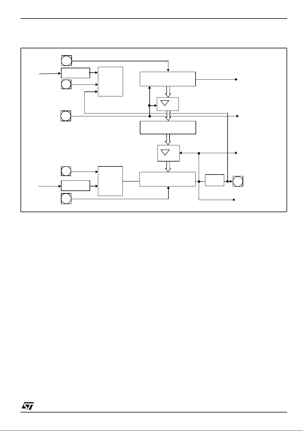
ST10F269 10 - GENERAL PURPOSE TIMER UNIT
Figure 16 : Block Diagram of GPT2
T5EUD
CPU Clock
T5IN
CAPIN
T6IN
CPU Clock
T6EUD
2n n=2...9
n
2
n=2...9
T5
Mode
Control
T6
Mode
Control
Clear
Capture
U/D
GPT2 Timer T5
GPT2 CAPREL
GPT2 Timer T6
U/D
Reload
Toggle FF
T60TL
Interrupt
Request
Interrupt
Request
Interrupt
Request
T6OUT
to CAPCOM
Timers
55/184

11 - PWM MODULE ST10F269
11 - PWM MODULE
The pulse width modulation module can generate
up to four PWM output signals using edge-aligned
or centre-aligned PWM. In addition, the PWM
module can generate PWM burst signals and
Figure 17 : Block Diagram of PWM Module
single shot outputs. Table 16 and Ta ble 17 show
the PWM frequencies for different resolutions. The
level of the output signals is selectable and the
PWM module can generate interrupt requests.
*
*
*
Match
Match
Clear Control
Output Control
Write Control
Up/Down/
POUTx
Enable
Clock 1
Clock 2
User readable / writeable register
*
Input
Control
Run
PPx Period Register
Comparator
PTx
16-bit Up/Down Counter
Comparator
Shadow Register
PWx Pulse Width Register
Table 16 : PWM Unit Frequencies and Resolution at 40MHz CPU Clock (PQFP144 devices)
Mode 0 Resolution 8-bit 10-bit 12-bit 14-bit 16-bit
CPU Clock/1 25ns 156.25kHz 39.1kHz 9.77kHz 2.44Hz 610Hz
CPU Clock/64 1.6 µs 2.44Hz 610Hz 152.6Hz 38.15Hz 9.54Hz
Mode 1 Resolution 8-bit 10-bit 12-bit 14-bit 16-bit
CPU Clock/1 25ns 78.12kHz 19.53kHz 4.88kHz 1.22kHz 305.17Hz
CPU Clock/64 1.6 µs 1.22kHz 305.17Hz 76.29Hz 19.07Hz 4.77Hz
Table 17 : PWM Unit Frequencies and Resolution at 32MHz CPU Clock (TQFP144 devices)
Mode 0 Resolution 8-bit 10-bit 12-bit 14-bit 16-bit
CPU Clock/1 31.25ns 125KHz 31.25KHz 7.81KHz 1.953KHz 976.6Hz
CPU Clock/64 2.00 µs 1.953KHz 488.3Hz 122.1Hz 30.52Hz 7.63Hz
Mode 1 Resolution 8-bit 10-bit 12-bit 14-bit 16-bit
CPU Clock/1 31.25ns 62.5KHz 15.62KHz 3.90KHz 976.6Hz 244.1Hz
CPU Clock/64 2.00 µs 976.6Hz 244.1Hz 61Hz 15.26Hz 3.81Hz
56/184

ST10F269 12 - PARALLEL PORTS
12 - PARALLEL PORTS
12.1 - Introduction
The ST10F269 M CU provides up to 111 I/O lines
with programmable features. These capabilities
bring very flexible adaptation of this MCU t o wide
range of applications.
ST10F269 has 9 groups of I/O lines gathered as
following:
– Port 0 is a 2 time 8-bit port named P 0L (Low as
less significant Byte) and P0H (high as most sig-
nificant Byte)
– Port 1 is a 2 time 8-bit port named P1L and P1H
– Port 2 is a 16-bit port
– Port 3 is a 15-bit port (P3.14 l ine is not imple-
mented)
– Port 4 is a 8-bit port
– Port 5 is a 16-bit port input only
– Port 6, Port 7 and Port 8 are 8-bit port
These ports may be used as general purpose
bidirectional input or output, software controlled
with dedicated registers.
For example the output drivers of six of the por ts
(2, 3, 4, 6, 7, 8) can be configured (bit-wise) for
push-pull or open drain operation using ODPx
registers.
In addition, the sink and the s ource c apability a nd
the rise / fall time of the transition of the signal of
some of the push-pull buffers can be programmed
to fit the driving requirements of the application
and to minimize EM I. T his feature is i mp lem ented
on Port 0, 1, 2, 3 , 4, 6, 7 and 8 with the control
registers POCONx. The output drivers capabilities
of ALE, RD
, WR control lines are programmable
with the dedicated bits of POCON20 control
register.
The input threshold levels are programmable
(TTL/CMOS) for 5 por ts (2, 3, 4, 7, 8). T he logic
level of a pin is clocked into the input latch once
per state time, regardless whether the port is
configured for input or output. The threshold is
selected with the PICON register control bits.
A write operation to a port pin configured as an
input causes the value to be written into the por t
output latch, while a read operation returns the
latched state of the pin itself. A read-modify-write
operation reads the value of the pin, modifies it,
and writes it back to the output latch.
Writing to a pin configured as an output
(DPx.y=‘1’) causes the output latch and the pin t o
have the written value, since the out put buffer is
enabled. Reading this pin returns the value of the
output latch. A read-modify-write operation reads
the value of the output latch, modifies it, and
writes it back to the output latch, thus also
modifying the level at the pin.
I/O lines support an alternate function which is
detailed in the following description of each port.
57/184

12 - PARALLEL PORTS ST10F269
Figure 18 : SFRs and Pins Associated with the Parallel Ports
0
YPOCON0L
1
Y
2
Y
3
Y
4
Y
5
Y
6
Y
7
Y
-
8
-
9
-
10
11
12
13
14
Output Driver Control Register
15
0
1
2
3
4
5
6
7
8
9
10
11
12
13
14
Threshold / Open Drain Control
15
-
-
-
-
E
YPICON
Y
Y
Y
Y
Y
Y
-
-
-
-
-
-
-
E
- - - - YYYYYYYYPOCON0H
- - - - YYYYYYYYPOCON1L
----
----
E
E
----- - - - YYYYYYYYPOCON1H
E
Y YYYYYYYYYYYPOCON2
YYYY
Y-YYY YYYYYYYYYYYPOCON3
E
E
Y YYYYYYYYYYYODP2
--Y-Y YYYYYYYYYYYODP3
YYYY
E
E
- - - - YYYYYYYYPOCON4
---E
----YY------ODP4
Y YYYYYYYYYYYP5DIDIS
----
YYYY
E
- - - -YYYYYYYYPOCON6
- - - - YYYYYYYYPOCON7
----
----
E
E
- - - -YYYYYYYYODP6
- - - -YYYYYYYYODP7
----
----
E
E
- - - -YYYYYYYYPOCON20 *
----- - - -YYYYYYYYPOCON8
E
----- - - -YYYYYYYYODP8
E
----
E
, WR, ALE lines only
* RD
0
YDP0L
1
Y
2
Y
3
Y
4
Y
5
Y
6
Y
7
Y
-
8
-
9
-
10
11
12
13
Direction Control Registers
14
15
0
1
2
3
4
5
6
7
8
9
10
11
12
13
14
Data Input / Output Register
15
-
-
-
-
E
YP0L
Y
Y
Y
Y
Y
Y
Y
-
-
-
-
-
-
-
-
- - - - YYYYYYYYDP0H
- - - - YYYYYYYYDP1L
----
----
E
E
- - - - YYYYYYYYP0H
- - - - YYYYYYYYP1L
----
----
----- - - - YYYYYYYYDP1H
E
----- - - - YYYYYYYYP1H
Y YYYYYYYYYYYDP2
Y-YYY YYYYYYYYYYYDP3
YYYY
Y YYYYYYYYYYYP2
Y-YYY YYYYYYYYYYYP3
YYYY
- - - - YYYYYYYYDP4
----
- - - - YYYYYYYYP4
----
YYYYY YYYYYYYYYYYP5
- - - -YYYYYYYYDP6
- - - - YYYYYYYYDP7
----
----
- - - - YYYYYYYYP6
- - - - YYYYYYYYP7
----
----
----- - - -YYYYYYYYDP8
P3LIN P3HIN
P4LIN
P6LIN (to be implemented)
P7LIN
P8LIN
Register be longs to ESFR areaE:
----- - - - YYYYYYYYP8
PICON: P2LIN P2HIN
Y : Bit has an I/O function
- : Bit has no I/O dedicated function or is not implemented
58/184

ST10F269 12 - PARALLEL PORTS
12.2 - I/O’s Special Features
12.2.1 - Open Drain Mo de
Some of the I/O por ts of ST10F269 support the
open drain capability. This programmable feature
may be used with an externa l pull-up resistor, in
order to get an AND wired logical function.
12.2.2 - Input Threshold Control
The standard inputs of the ST10F269 determine
the status of input signals according to TTL levels.
In order to accept and recognize noisy signals,
CMOS-like input thresholds can be selected
instead of the standard TTL thresholds for all pins
of Port 2, Port 3, Port 4, Port 7 and Port 8. These
special thresholds are defined above the TTL
thresholds and feature a defined hysteresis to
This feature is implemented for ports P2, P3, P4,
P6, P7 and P8 (see respective sections), and is
controlled through the respective Open Drain
Control Registers ODPx. These registers allow
the individual bit-wise selection of the open drain
mode for each por t line. If the respective control
prevent the inputs from toggling while the
respective input signal level is near the thresholds.
The Port Input Control re gister PICON is used to
select these thresholds for each Byte of the
indicated por ts, this means the 8-bit po r ts P4, P7
and P8 are controlled by one bit eac h while por ts
P2 and P3 are controlled by two bits each.
bit ODPx.y is ‘0’ (default after reset), the output
driver is in the push-pull mode. If ODPx.y is ‘1’, the
open drain configuration is selected. Note that all
ODPx registers are located in the ESFR space
(See Figure 19).
All options for indi vidual direction and outpu t mode
control are available for each pin, independent of
the selected input threshold. The input hysteresis
provides stable inputs from noisy or slowly
changing external signals (See Figure 20).
PICON (F1C4h / E2h) ESFR Reset Value: --00h
1514131211109876543210
--------P8LINP7LIN-P4LINP3HINP3LINP2HINP2LIN
RW RW RW RW RW RW RW
Bit Function
PxLIN Port x Low Byte Input Level Selection
0: Pins Px.7...Px.0 switch on standard TTL input levels
1: Pins Px.7...Px.0 switch on special threshold input levels
PxHIN Port x High Byte Input Level Selection
0: Pins Px.15...Px.8 switch on standard TTL input levels
1: Pins Px.15...Px.8 switch on special threshold input levels
Figure 19 : Output Drivers in Push-pull Mode and in Open Drain Mode
Pin
Q
Push-Pull Output Driver
Q
Open Drain Output Driver
External
Pullup
Pin
59/184

12 - PARALLEL PORTS ST10F269
Figure 20 : Hysteresis for Special Input Thresholds
Hysteresis
Input level
Bit state
12.2.3 - Output Driver Control
The port output control registers POCONx allow
to select the por t out put driver cha racteristics of a
port. The aim of these selections is to adapt the
output drivers to the application’s requirements,
and to improve the EMI behaviour of the device.
Two characteristics may be selecte d :
Edge characteristic define s the rise/fall time for
the respective output. Slow edges reduce the
peak currents that are sinked/sourced when
changing the voltage level of an external
capacitive load. For a bus interf ace or pins that are
changing at frequency higher than 1MHz,
however, fast edges may still be required.
Driver characteristic defines either the general
drivin g capability of the respective driver, or if the
driver strength is reduced after the target output
level has been reached or not. Reducing the
driver strength increases the output’s internal
resistance, which attenuates noise that is
imported via the output line. For driving LEDs or
power transistors, however, a stable high output
current may still be required as described below.
This rise / fall time of 4 I/O pads (a nibble) is
selected using 2-bit named PNxEC. That means
Port Nibble (x = nibble number , it could be 3 as for
Port 2.15 to 2.12) Edge Characteristic.
The sink / source capability of the same 4 I/O
pads is selected using 2-bit named PNxDC. That
means Port Nibble (x = nibble number) Drive
Characteristic (See Table 18).
POCONx (F0yyh / zzh) for 8-bit Ports ESFR Reset Value: --00h
1514131211109876543210
--------PN1DC PN1EC PN0DC PN0EC
RW RW RW RW
POCONx (F0yyh / zzh) for 16-bit Ports ESFR Reset Value: 0000h
1514131211109876543210
PN3DC PN3EC PN2DC PN2EC PN1DC PN1EC PN0DC PN0EC
RW RW RW RW RW RW RW RW
Bit Function
PNxEC Port Nibble x Edge Characteristic (rise/fall time)
00: Fast edge mode, rise/fall times depend on the size of the driver.
01: Slow edge mode, rise/fall times ~60 ns
10: Reserved
11: Reserved
PNxDC Port Nibble x Driver Characteristic (output current)
00: High Current mode:
Driver always operates with maximum strength.
01: Dynamic Current mode:
Driver strength is reduced after the target level has been reached.
10: Low Current mode:
Driver always operates with reduced strength.
11: Reserved
Note: In case of reading an 8 bit P0CONX register, high Byte (bit 15..8) is read as 00h
60/184
ST10F269 12 - PARALLEL PORTS
The table lists the defined POCON registers and the allocation of control bit-fields and port pins.
Table 18 : Port Control Register Allocation
Control
Register
POCON0L F080h 40h P0L.7...4 P0L.3...0
POCON0H F082h 41h P0H.7...4 P0H.3...0
POCON1L F084h 42h P1L.7...4 P1L.3...0
POCON1H F086h 43h P1H.7...4 P1H.3...0
POCON2 F088h 44h P2.15...12 P2.11...8 P2.7...4 P2.3...0
POCON3 F08Ah 45h P3.15, 3.13, 3.12 P3.11...8 P3.7...4 P3.3...0
POCON4 F08Ch 46h P4.7...4 P4.3...0
POCON6 F08Eh 47h P6.7...4 P6.3...0
POCON7 F090h 48h P7.7...4 P7.3...0
POCON8 F092h 49h P8.7...4 P8.3...0
Physical
Address
8-bit
Address
3
Controlled Port Nibble
210
Dedicated Pins Output Control
Programmable pad drivers also are supported for the dedicated pins ALE, RD
and WR. For these pads, a
special POCON20 register is provided.
POCON20 (F0AAh / 55h) ESFR Reset Value: --00h
1514131211109876543210
--------PN1DC PN1EC PN0DC PN0EC
RW RW RW RW
PN0EC RD, WR Edge Characteristic (rise/fall time)
00: Fast edge mode, rise/fall times depend on the size of the driver.
01: Slow edge mode, rise/fall times ~60 ns
10: Reserved
11: Reserved
PN0DC RD
, WR Driver Characteristic (output current)
00: High Current mode:
Driver always operates with maximum strength.
01: Dynamic Current mode:
Driver strength is reduced after the target level has been reached.
10: Low Current mode:
Driver always operates with reduced strength.
11: Reserved
PN1EC ALE Edge Characteristic (rise/fall time)
00: Fast edge mode, rise/fall times depend on the size of the driver.
01: Slow edge mode, rise/fall times ~60 ns
10: Reserved
11: Reserved
PN1DC ALE Driver Characteristic (output current)
00: High Current mode:
Driver always operates with maximum strength.
01: Dynamic Current mode:
Driver strength is reduced after the target level has been reached.
10: Low Current mode:
Driver always operates with reduced strength.
11: Reserved
61/184

12 - PARALLEL PORTS ST10F269
12.2.4 - Alternate Port Functions
Each por t line h as one as sociated programmable
alternate input or output function.
– PORT0 and PORT1 may be used as address
and data lines when acces sing external memory .
– Port 2, Port 7 and Port 8 are associated with the
capture inputs or compare outputs of the CAPCOM units and/or with the outputs of the PWM
module.
Port 2 is also used for fast external interrupt inputs and for timer 7 input.
– Port 3 includes the alternate functions of timers,
serial interfaces, the optional bu s control signa l
BHE
and the system clock output (CLKOUT).
– Port 4 outputs the additional segment address
bit A16 to A23 in systems where segm entation
is enabled to access more than 64K Bytes of
memory.
– Port 5 is used as analog input channels of the
A/D converter or as timer c ontrol signals.
– Port 6 provides optional bus arbitration signals
(BREQ
, HLDA, HOLD) and chip select signals.
If an alternate output function of a pin is to be
used, the direction of this pin must be
programmed for output (DPx.y=‘1’), except for
some signals that are used directly after reset and
are configured automatically. Otherwise the pin
remains in the high-impedance state and is not
effected by the alternate output function. The
respective port latch should hold a ‘1’, because its
output is ANDed with the alternate output data
(except for PWM output signals).
If an alter nate input function of a pin is used, the
direction of the pin must be programmed for input
(DPx.y=‘0’) if an external device is dr iving the pin.
The input direction is the default after reset. If no
external device is connected to the pin, however,
one can also set the direction for this pin to output.
In this case, the pin reflects the state of the port
output latch. Thus, the alternate input function
reads the value stored in the port output latch.
This can be us ed for testing purposes to allow a
software trigger of an alternate input function by
writing to the port output latch.
On most of the port lines, the application software
must set the proper direction when using an
alternate input or output function of a pin. This is
done by setting or clearing the direction control bit
DPx.y of the pin before enabling the alternate
function. There are port lines, however, where t he
direction of the port line is switched automatically.
For instance, in the multiplexed external bus
modes of P ORT0, the direction must be switched
several times for an instruction fetch in order to
output the addresses and to input the data.
Obviously, this cannot be done through
instructions. In these cases, the direction of the
port li ne is switched automatically by hardware if
the alternate function of such a pin is enabled.
To determine the appropriate level of the port
output latches check how the alternate data
output is combined with the respective port latch
output.
There is one basic structure for all port lines
support ing only one alternate input function. Port
lines with only one alternate output function,
however, have different structures. It has to be
adapted to suppor t the normal and the alternate
function features.
All port lines that are not used for these alternate
functions may be used as general purpose I/O
lines. When using port pins for general purpose
output, the initial output value should be written to
the port latch prior to enabling the output drivers,
in order to avoid undesired transitions on the
output pins. This applies to single pins as well as
to pin groups (see examples below).
SINGLE_BIT: BSET P4.7 ; Initial output level is "high"
BSET DP4.7 ; Switch on the output driver
BIT_GROUP: BFLDH P4, #24H, #24H ; Initial output level is "high"
BFLDH DP4, #24H, #24H ; Switch on the output drivers
Note: When using several BSET pairs to control more pins of one port, these pairs must be separated by
instructions, which do not ap ply to the respective port (See C hapter : Central Processing Unit
(CPU) on page 35).
62/184

ST10F269 12 - PARALLEL PORTS
12.3 - PORT0
The two 8-bit ports P0H and P0L represent the
higher and lower part of PORT0, respectively.
Both halves of PORT0 can be written (via a PEC
transfer) without effecting the other half.
P0L (FF00h / 80h) SFR Reset Value: --00h
1514131211109876543210
--------P0L.7P0L.6P0L.5P0L.4P0L.3P0L.2P0L.1P0L.0
P0H (FF02h / 81h) SFR Reset Value: --00h
1514131211109876543210
--------P0H.7P0H.6P0H.5P0H.4P0H.3P0H.2P0H.1P0H.0
P0X.y Port Data Register P0H or P0L Bit y
DP0L (F100h / 80h) ESFR Reset Value: --00h
1514131211109876543210
--------DP0L.7DP0L.6DP0L.5DP0L.4DP0L.3DP0L.2DP0L.1DP0L.0
RW RW RW RW RW RW RW RW
If this port is used for general purpose I/O, the
direction of each line can be configured via the
corresponding direction registers DP0H and
DP0L.
RW RW RW RW RW RW RW RW
RW RW RW RW RW RW RW RW
DP0H (F102h / 81h) ESFR Reset Value: --00h
1514131211109876543210
--------DP0H.7DP0H.6DP0H.5DP0H.4DP0H.3DP0H.2DP0H.1DP0H.0
RW RW RW RW RW RW RW RW
DP0X.y Port Direction Register DP0H or DP0L Bit y
DP0X.y = 0: Port line P0X.y is an input (high-impedance)
DP0X.y = 1: Port line P0X.y is an output
63/184

12 - PARALLEL PORTS ST10F269
12.3.1 - Alternate Functions of PORT0
When an exter nal bus is enabled, PORT0 is used
as data bus or address/data bus.
Note that an external 8-bi t demul tiplexed bus only
uses P0L, while P0H is free for I/O (provided that
no other bus mode is enabled).
PORT0 is also used to select t he system sta rt -up
configuration. During res et, PORT0 is configured
to input, and each line is held high through an
internal pull-up device.
Each line can now be individually pulled to a low
level (see Section 21.3 -: DC Characteristics)
through an external pull-down device. A default
configuration is selected when the respective
PORT0 lines are at a high level. Through pulling
individual lines to a low level, this default can be
changed according to the needs of the
applications.
The interna l pull-up devices are designed in s uch
way that an external pull-down resistors (see Data
Sheet specification) can be used to apply a
correct low level.
These external pull-down resistors can remain
connected to the PORT0 p ins also d uring nor mal
operation, however, care has to be taken in order
to not disturb the no rmal function of PORT0 (this
might be the case, for example, if the external
resistor value is too low).
Figure 21 : PORT0 I/O and Alternate Functions
With the end of reset, the selected bus
configuration will be written to the BUSCON0
register.
The configuration of t he high byte of PORT0, will
be copied into the special register RP0H. This
read-only register holds the selection for the
number of chip selects and segment addresses.
Software can read this register in order to react
according to the selected configuration, if
required.
When the reset is termina ted, the internal pull-up
devices are switched off, and PORT0 will be
switched to the appropriate operating mode.
During external accesses in multiplexed bus
modes PORT0 first outputs the 16-bit
intra-segment address as an alternate output
function. PORT0 is then switched to
high-impedance i nput mode to read the incoming
instruction or data. In 8-bit data bus mode, two
memory cycles are required for word accesses,
the first for the low Byte and the seco nd for the
high Byte of the Word.
During write cycles PORT0 outputs the data Byte
or Word after outputting the address. During
external accesses in demultiplexed bus modes
PORT0 reads the incoming instruction or data
Word or outputs the data Byte or Word.
Alternate Function a) b) c) d)
P0H
PORT0
P0L
General Purpose
Input/Output
P0H.7
P0H.6
P0H.5
P0H.4
P0H.3
P0H.2
P0H.1
P0H.0
P0L.7
P0L.6
P0L.5
P0L.4
P0L.3
P0L.2
P0L.1
P0L.0
D7
D6
D5
D4
D3
D2
D1
D0
8-bit
Demultiplexed Bus
Demultipl exed Bus
16-bit
D15
D14
D13
D12
D11
D10
D9
D8
D7
D6
D5
D4
D3
D2
D1
D0
A15
A14
A13
A12
A11
A10
A9
A8
AD7
AD6
AD5
AD4
AD3
AD2
AD1
AD0
8-bit
Multipl exed Bu s
AD15
AD14
AD13
AD12
AD11
AD10
AD9
AD8
AD7
AD6
AD5
AD4
AD3
AD2
AD1
AD0
16-bit
Multipl exed Bus
64/184
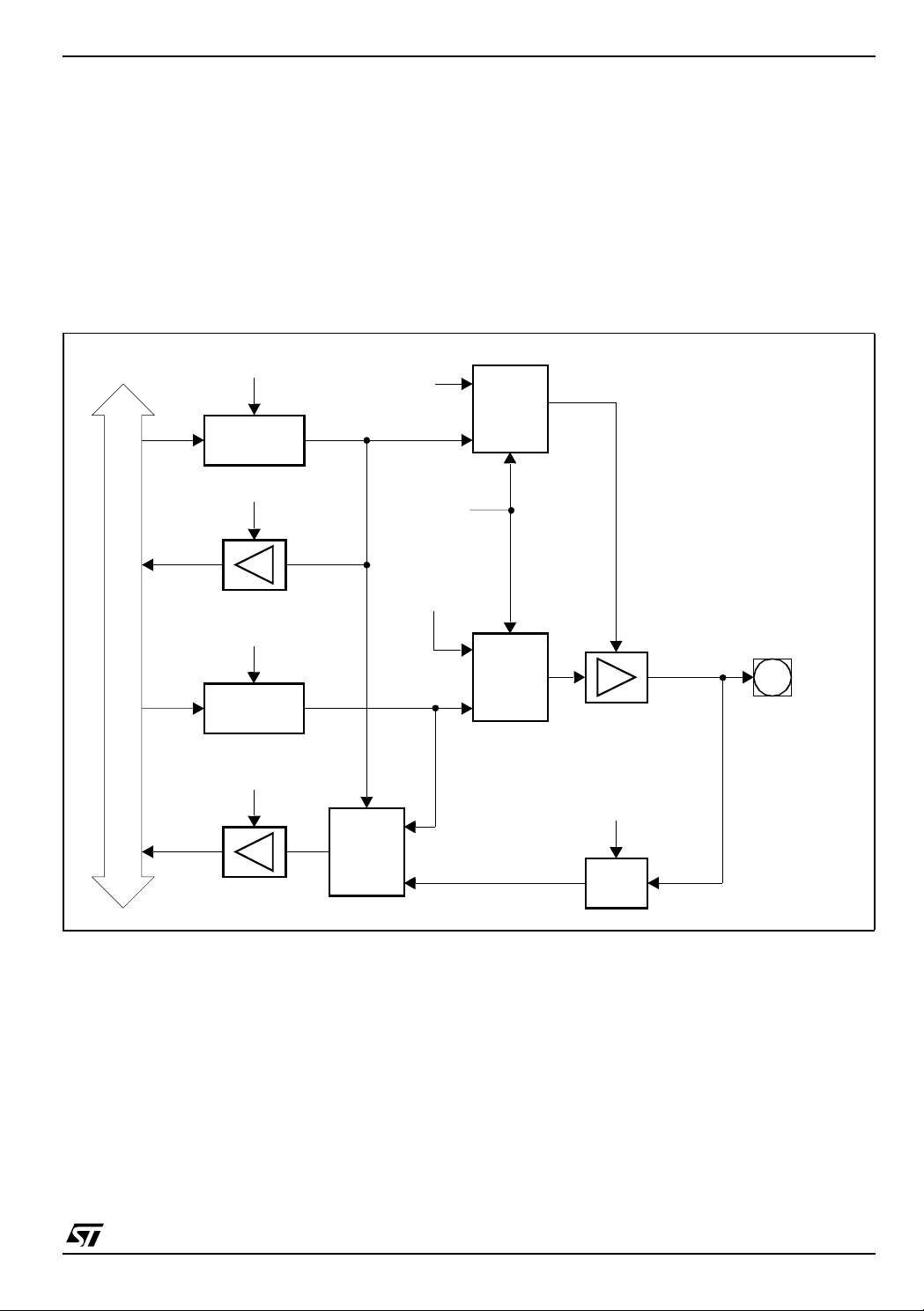
ST10F269 12 - PARALLEL PORTS
When an external bus mode is enabled, the
direction of the port pin and the loading of data
into the port output latch are controlled by the bus
controller hardware.
The input of the port output Buffer is disconnected
from the internal bus and is switched to the line
labeled “Alternate Data Output” via a multiplexer.
The alternate data can be the 16-bit intra-segment
address or the 8/16-bit data information. The
incoming data on PORT0 is read on the line
Figure 22 : Block Diagram of a PORT0 Pin
Write DP0H.y / DP0L.y
Direction
Latch
Read DP0H.y / DP0L.y
Alternate
Direction
Alternate
Function
Enable
Alternate
Data
Output
“Alternate Data Input”. While an external bus
mode is enabled, the user software should not
write to the port output latch, otherwise
unpredictable results may occur.
When the external bus modes are disabled, the
contents of the direction register last written by the
user becomes active.
The Figure 22 shows the structure of a PORT0
pin.
1
MUX
0
Write P0H.y / P0L.y
Internal Bus
Read P0H.y / P0L.y
Port Output
Latch
MUX
Port Data
Output
1
0
1
MUX
0
Clock
Input
Latch
Output
Buffer
P0H.y
P0L.y
y = 7...0
65/184

12 - PARALLEL PORTS ST10F269
12.4 - PORT1
The two 8-bit ports P1H and P1L represent the higher and lower part of PORT1, respectively . Both halves
of PORT1 can be written (via a PEC transfer) without effecting the other half.
If this port is used for general purpose I/O, the direction of each line can be configured via the
corresponding direction registers DP1H and DP1L.
P1L (FF04h / 82h) SFR Reset Value: --00h
1514131211109876543210
--------P1L.7P1L.6P1L.5P1L4P1L.3P1L.2P1L.1P1L.0
RW RW RW RW RW RW RW RW
P1H (FF06h / 83h) SFR Reset Value: --00h
1514131211109876543210
--------P1H.7P1H.6P1H.5P1H.4P1H.3P1H.2P1H.1P1H.0
RW RW RW RW RW RW RW RW
P1X.y Port Data Register P1H or P1L Bit y
DP1L (F104h / 82h) ESFR Reset Value: --00h
1514131211109876543210
- - - - - - - - DP1L.7 DP1L.6 DP1L.5 DP1L.4 DP1L.3 DP1L.2 DP1L.1 DP1L.0
RW RW RW RW RW RW RW RW
DP1H (F106h / 83h) ESFR Reset Value: --00h
1514131211109876543210
- - - - - - - - DP1H.7 DP1H.6 DP1H.5 DP1H.4 DP1H.3 DP1H.2 DP1H.1 DP1H.0
RW RW RW RW RW RW RW RW
DP1X.y Port Direction Register DP1H or DP1L Bit y
DP1X.y = 0: Port line P1X.y is an input (high-impedance)
DP1X.y = 1: Port line P1X.y is an output
12.4.1 - Alternate Functions of PORT1
When a demultiplexed external bus is enabled, PORT1 is used as address bus.
Note: Demultiplexed bus modes use PORT1 as a 16 -bit port. Otherwise all 16 port lines c an be us ed for
general purpose I/O.
The upper 4 pins of PORT1 (P1H.7...P1H.4) are used as capture input lines (CC27IO...CC24IO).
During external access es in demultiplexed bus modes PORT1 outputs the 16-bit intra-segm ent address
as an alternate output function.
During external accesses in multiplexed bus modes, when no BUSCON register selects a demultiplexed
bus mode, PORT1 is not used and is available for general purpose I/O.
66/184
ST10F269 12 - PARALLEL PORTS
Figure 23 : PORT1 I/O and Alternate Functions
Alternate Function a)
P1H.7
P1H.6
P1H.5
P1H
PORT1
P1L
General Purpose Input/Output 8/16-bit Demultiplexed Bus
P1H.4
P1H.3
P1H.2
P1H.1
P1H.0
P1L.7
P1L.6
P1L.5
P1L.4
P1L.3
P1L.2
P1L.1
P1L.0
When an external bus mode is enabled, the
direction of the port pin and the loading of data
into the port output latch are controlled by the bus
controller hardware.
The input of the por t B uffer latch is disconnected
from the internal bus and is switched to the line
labeled “Alternate Data Output” via a multiplexer.
The alternate data is the 16-bit intra-segment
b)
A15
A14
A13
A12
A11
A10
A9
A8
A7
A6
A5
A4
A3
A2
A1
A0
CAPCOM2 Capture Inputs only
CC27IO
CC26IO
CC25IO
CC24IO
address. While an external bus mode is enabled,
the user software should not write to the port
output latch, otherwise unpredictable results may
occur. When the external bus modes are disabled,
the contents of the direction register last written by
the user becomes active.
The Figure 24 shows the structure of a PORT1
pin.
Figure 24 : Block Diagram of a PORT1 Pin
Write DP1H.y / DP1L.y
Direction
Latch
Read DP1H .y / DP1L.y
Write P1H.y / P1L.y
Internal Bus
Port Outpu t
Latch
Read P1H.y / P1L.y
MUX
“1”
Alternate
Function
Enable
Alternate
Data
Output
Port Data
Output
1
0
1
MUX
0
1
MUX
0
Clock
Input
Latch
Output
Buffer
P1H.y
P1L.y
y = 7...0
67/184

12 - PARALLEL PORTS ST10F269
12.5 - Port 2
If this 16-bit por t is used for general purpose I/O, the direction of each line can be configured via the
corresponding direction regi ster DP2. Each por t line can be switched into push/ pull or op en drain mode
via the open drain control register ODP2.
P2 (FFC0h / E0h) SFR Reset Value: 0000h
1514131211109876543210
P2.15 P2.14 P2.13 P2.12 P2.11 P2.10 P2.9 P2.8 P2.7 P2.6 P2.5 P2.4 P2.3 P2.2 P2.1 P2.0
RW RW RW RW RW RW RW RW RW RW RW RW RW RW RW RW
P2.y Port Data Register P2 Bit y
DP2 (FFC2h / E1h) SFR Reset Value: 0000h
1514131211109876543210
DP2
DP2
DP2
DP2
DP2
DP2
DP2.9DP2.8DP2.7DP2.6DP2.5DP2.4DP2.3DP2.2DP2.1DP2
.15
.14
.13
.12
.11
.10
RW RW RW RW RW RW RW RW RW RW RW RW RW RW RW RW
DP2.y Port Direction Register DP2 Bit y
DP2.y = 0: Port line P2.y is an input (high-impedance)
DP2.y = 1: Port line P2.y is an output
.0
ODP2 (F1C2h / E1h) ESFR Reset Value: 0000h
1514131211109876543210
ODP2
ODP2
ODP2
ODP2
ODP2
ODP2
ODP2.9ODP2.8ODP2.7ODP2.6ODP2.5ODP2.4ODP2.3ODP2.2ODP2.1ODP2
.15
.14
.13
.12
.11
.10
RW RW RW RW RW RW RW RW RW RW RW RW RW RW RW RW
.0
ODP2.y Port 2 Open Drain Con trol Register Bit y
ODP2.y = 0: Port line P2.y output driver in push/pull mode
ODP2.y = 1: Port line P2.y output driver in open drain mode
12.5.1 - Alternate Functions of Port 2
All Port 2 lines (P2.15...P2.0) serve as capture
inputs or compa re outputs (CC15IO...CC0IO) for
the CAPCOM1 unit.
When a Port 2 line is used as a capture input, the
state of the input latch, which represents the state
of the port pin, is directed to the CAPCOM unit via
the line “Alternate Pin Data Input”. If an external
capture trigger signal is used, the direction of the
respective pin must be set to input.
If the direction is set to output, the state of the port
output latch will be read since the pin represents
the state of the output latch.
This can be used to trigger a capture event
through software by setting or clearing the port
latch. Note that in the output configuration, no
external device may drive the pin, otherwise
conflicts would occur.
When a Port 2 line is used as a compare output
(compare modes 1 and 3), the co mpare event (or
the timer overflow in compare mode 3) directly
effects the port output latc h. In compare mode 1,
when a valid compare match occurs, the st ate of
the port output latch is read by the CAPCOM
control hardware via the line “Alternate Latch Data
Input”, inverted, and written back to the latch via
the line “Alternate Data Output”.
The port output latch is clocked by the signal
“Compare Trigger” which is generated by the
CAPCOM unit. In compare mode 3, when a match
occurs, the value '1' is written to the port output
latch via the li ne “Alternate Data Output”. When
an overflow of the corresponding timer occurs, a
'0' is written to the port output latch. In both cases,
68/184

ST10F269 12 - PARALLEL PORTS
the output latch is clocked by the signal “Compare
Trigger”.
The direction of the pin should be set to output by
the user, otherwise the pin will be in the
high-impedanc e stat e and will not refl ect the stat e
of the output latch.
As can be seen from the port structure in
Figure 26, the user software always has free
access to the port pin even when it is used a s a
compare output. This is useful for setting up the
initial level of the pin when using compare mode 1
or the double-register mode. In these modes,
unlike in compare m ode 3, the p in is not set to a
specific value when a compare match occurs, but
is toggled instead.
When the user wants to write to the port pin at the
same time a compare trigger tries to clock the
output latch, the write operation of the user
software has priority. Each time a CPU write
access to the por t output latch occurs, the input
multiplexer of the port output latch is switched to
the line connected to the internal bus. The port
output latch will receive the value from the internal
bus and the hardware triggered change will be
lost.
As all other capture inputs, the capture input
function of pins P2.15 ...P2.0 can also be u sed as
external interrupt inputs (200ns sample rate at
40MHz CPU clock on PQFP144 devices and
250ns sample rate at 32MHz CPU clock on
TQFP14 4 devices).
The upper eight Port 2 lines (P2.15...P2.8) also
can serve as Fast External Interru pt inputs from
EX0IN to EX7IN (Fast external interrupt sampling
rate is 25ns at 40MHz CPU cl ock and 31.25ns at
32MHz CPU clock).
P2.15 in addition serves as input for CAPCOM2
timer T7 (T7IN). The Table 19 summarizes the
alternate functions of Port 2.
Table 19 : Alternate Functions of Port 2
Port 2 Pin Alternate Function a) Alternate Function b) Alternate Function c)
P2.0
P2.1
P2.2
P2.3
P2.4
P2.5
P2.6
P2.7
P2.8
P2.9
P2.10
P2.11
P2.12
P2.13
P2.14
P2.15
CC0IO
CC1IO
CC2IO
CC3IO
CC4IO
CC5IO
CC6IO
CC7IO
CC8IO
CC9IO
CC10IO
CC11IO
CC12IO
CC13IO
CC14IO
CC15IO
-
-
-
-
-
-
-
EX0IN Fast External Interrupt 0 Input
EX1IN Fast External Interrupt 1 Input
EX2IN Fast External Interrupt 2 Input
EX3IN Fast External Interrupt 3 Input
EX4IN Fast External Interrupt 4 Input
EX5IN Fast External Interrupt 5 Input
EX6IN Fast External Interrupt 6 Input
EX7IN Fast External Interrupt 7 Input
-
-
-
-
-
-
-
-
-
-
-
-
-
-
T7IN T7 External Count Input
69/184

12 - PARALLEL PORTS ST10F269
Figure 25 : Port 2 I/O and Alternate Functions
Alternate Function a)
P2.15
P2.14
P2.13
P2.12
P2.11
P2.10
P2.9
Port 2
General Purpose
Input / Output
P2.8
P2.7
P2.6
P2.5
P2.4
P2.3
P2.2
P2.1
P2.0
CAPCOM1
Capture Input / Compare Output
CC15IO
CC14IO
CC13IO
CC12IO
CC11IO
CC10IO
CC9IO
CC8IO
CC7IO
CC6IO
CC5IO
CC4IO
CC3IO
CC2IO
CC1IO
CC0IO
b)
Fast Extern al
Interrupt Input
EX7IN
EX6IN
EX5IN
EX4IN
EX3IN
EX2IN
EX1IN
EX0IN
Timer T7 Input
c)
T7IN
CAPCOM2
70/184

ST10F269 12 - PARALLEL PORTS
The pins of Port 2 combine internal bus data with alternate data output before the port latch input.
Figure 26 : Block Diagram of a Port 2 Pin
Write ODP2.y
Open Drain
Latch
Read ODP2.y
Write DP2.y
Direction
Latch
Internal Bu s
Alternate
Data
Output
Write Po rt P 2 .y
Compare Trigger
Read DP2.y
1
MUX
0
Read P2.y
Output
Latch
≥
1
MUX
Alternate Data Input
Fast External Interrupt Input
P2.y
Output
Buffer
Clock
1
0
Input
Latch
CCyIO
EXxIN
x = 7...0
y = 15...0
12.6 - Port 3
If this 15-bit por t is used for general purpose I/O,
the direction of each line can be configured by the
corresponding direction register DP3. Most port
lines can be switched into pus h-pull or open drain
mode by the open drain control register ODP2
71/184

12 - PARALLEL PORTS ST10F269
(pins P3.15, P3.14 and P3.12 do not support open
drain mode).
Due to pin limitations register bit P3.14 is not
connected to an output pi n.
P3 (FFC4h / E2h) SFR Reset Value: 0000h
1514131211109876543210
P3.15 - P3.13 P3.12 P3.11 P3.10 P3.9 P3.8 P3.7 P3.6 P3.5 P3.4 P3.3 P3.2 P3.1 P3.0
RW RW RW RW RW RW RW RW RW RW RW RW RW RW RW RW
P3.y P o rt Data Register P3 Bit y
DP3 (FFC6h / E3h) SFR Reset Value: 0000h
1514131211109876543210
DP3
.15
RW RW RW RW RW RW RW RW RW RW RW RW RW RW RW RW
-DP3
.13
DP3
.12
DP3
.11
DP3
DP3.9DP3.8DP3.7DP3.6DP3.5DP3.4DP3.3DP3.2DP3.1DP3
.10
.0
DP3.y Port Direction Register DP3 Bit y
DP3.y = 0: Port line P3.y is an input (high-impedance)
DP3.y = 1: Port line P3.y is an output
ODP3 (F1C6h / E3h) ESFR Reset Value: 0000h
1514131211109876543210
--ODP3
.13
RW RW RW RW RW RW RW RW RW RW RW RW RW RW RW RW
-ODP3
ODP3
.11
ODP3.9ODP3.8ODP3.7ODP3.6ODP3.5ODP3.4ODP3.3ODP3.2ODP3.1ODP3
.10
.0
ODP3.y Port 3 Open Drain Control Register Bit y
ODP3.y = 0: Port line P3.y output driver in push-pull mode
ODP3.y = 1: Port line P3.y output driver in open drain mode
72/184

ST10F269 12 - PARALLEL PORTS
12.6.1 - Alternate Functions of Port 3
The pins of Port 3 serve for various functions which include external timer control lines, the two serial
interfaces and the control lines BHE
Table 20 : Port 3 Alternat ive Functions
Port 3 Pin Alternate Function
/WRH and CLKOUT.
P3.0
P3.1
P3.2
P3.3
P3.4
P3.5
P3.6
P3.7
P3.8
P3.9
P3.10
P3.11
P3.12
P3.13
P3.14
P3.15
T0IN CAPCOM1 Timer 0 Count Input
T6OUT Timer 6 Toggle Output
CAPIN GPT2 Capture Input
T3OUT Timer 3 Toggle Output
T3EUD Timer 3 External Up/Down Input
T4IN Timer 4 Count Input
T3IN Timer 3 Count Input
T2IN Timer 2 Count Input
MRST SSC Master Receive / Slave Transmit
MTSR SSC Master Transmit / Slave Receive
TxD0 ASC0 Transmit Data Output
RxD0 ASC0 Receive Data Input (Output in synchronous mode)
BHE
/WRH Byte High Enable / Write High Output
SCLK SSC Shift Clock Input/Output
--- No pin assigned
CLKOUT System Clock Output
Figure 27 : Port 3 I/O and Alternate Functions
Alternate Function a) b)
No Pin
Port 3
General Purpose Input/Output
P3.15
P3.13
P3.12
P3.11
P3.10
P3.9
P3.8
P3.7
P3.6
P3.5
P3.4
P3.3
P3.2
P3.1
P3.0
CLKOUT
SCLK
BHE
RxD0
TxD0
MTSR
MRST
T2IN
T3IN
T4IN
T3EUD
T3OUT
CAPIN
T6OUT
T0IN
WRH
The structure of the Port 3 p ins depends on their
alternate function (see figures Figure 28 and
Figure 29). When the on-chip peripheral
associated with a Port 3 pin is configured to use
the alternate input function, it reads the input
latch, which represents the state of the pin, via the
line labeled “Alternate Data Input”. Port 3 pins with
alternate input functions are: T0IN, T2IN, T3IN,
T4IN, T3EUD and CAPIN.
When the on-chip peripheral associated with a
Port 3 pin is configured to use the alternate output
function, its “Alternate Data Output” line is ANDed
with the port output latch line. When using these
alternate functions, the user must set the direction
of the port line to output (DP3.y=1) and must set
the port output latch (P3.y=1). Otherwise the pin is
in its high-impedance st ate (when configured as
input) or the pin is stuck at '0' (when the port
output latch is cleared). When the alternate output
functions are not used, the “Alternate Data
Output” line is in its inactive state, which is a high
level ('1').
Port 3 pins with alternate output functions are:
T6OUT, T3OUT, TxD0, BH E
and CLKOUT.
73/184

12 - PARALLEL PORTS ST10F269
When the on-chip peripheral associated with
a Port 3 pin is configured to use both the alternate
input and output function, the de scriptions above
apply to the respective current operating mode.
The direction must be set accordingly. Port 3 pins
with alternate input/output functions are: MTSR,
MRST, RxD0 and SCLK.
Note: Enabling the CLKOUT function automati-
cally enables the P3.15 output driver. Setting bit DP3.15=’1’ is not required.
Figure 28 : Block Diagram of Port 3 Pin with Alternate Input or Alternate Output Function
Write ODP3.y
Open Drain
Latch
Read ODP3.y
Write DP3.y
Internal Bus
Direction
Latch
Read DP3.y
Write DP3.y
Port Output
Latch
Read P3.y
MUX
Alternate
Data
Input
Alternate
Data Output
Port Data
Output
1
0
&
Output
Buffer
Clock
Input
Latch
y = 13, 11...0
P3.y
74/184

ST10F269 12 - PARALLEL PORTS
Pin P3.12 (BHE/WRH) is another pin with an
alternate output function, however, its structure is
slightly different.
After reset the BHE
or WRH function must be
used depending on the system start-up
configuration. In either of thes e ca ses, there is no
possibility to program any port latches before.
Thus, the appropriate alternate function is
selected automatically. If BHE
the system, this pin can be used for general
purpose I/O by disabling the alternate function
(BYTDIS = ‘1’ / WRCFG=’0’).
Figure 29 : Block Diagram of Pins P3.15 (CLKOUT) and P3.12 (BHE
Write DP3.x
“1”
Direction
Latch
Read DP3.x
Alternate
Function
Enable
Write P3.x
Internal Bus
Port Output
Latch
Alternate
Data
Output
1
MUX
0
1
MUX
0
/WRH)
Output
Buffer
/WRH is not used in
P3.12/BHE
P3.15/CLKOUT
Read P3.x
Note: Enabling the BHE
DP3.12=’1’ is not required.
During bus hold pin P3.12 is switched back to its standard function and is then controlled by
DP3.12 and P3.12. Keep DP3.12 = ’0’ in this case to ensure floating in hold mode.
Clock
1
MUX
0
Input
Latch
x = 15, 12
or WRH function automatically enables the P3.12 output driver. Setting bit
75/184

12 - PARALLEL PORTS ST10F269
12.7 - Port 4
If this 8-bit por t is used for general purpose I/O, the direction of eac h line can be configured via the
corresponding direction register DP4.
P4 (FFC8h / E4h) SFR Reset Value: --00h
1514131211109876543210
- - - - - - - - P4.7 P4.6 P4.5 P4.4 P4.3 P4.2 P4.1 P4.0
RW RW RW RW RW RW RW RW
P4.y P o rt Data Register P4 Bit y
DP4 (FFCAh / E5h) SFR Reset Value: --00h
1514131211109876543210
--------DP4.7DP4.6DP4.5DP4.4DP4.3DP4.2DP4.1DP4.0
RW RW RW RW RW RW RW RW
DP4.y Port Direction Register DP4 Bit y
DP4.y = 0: Port line P4.y is an input (high-impedance)
DP4.y = 1: Port line P4.y is an output
For CAN configuration support (see sec tion 15), Port 4 has an open drain function, controlled with the
ODP4 r egister:
ODP4 (F1CAh / E5h) ESFR Reset Value: --00h
15 14 13 12 11 10 9 8 7 6 5 4 3 2 1 0
- - - - - - - - ODP4.7 ODP4.6 - - - - - RW RW
ODP4.y Port 4 Open Drain Control Register Bit y
ODP4.y = 0: Port line P4.y output driver in push/pull mode
ODP4.y = 1: Por t line P4. y ou tput driver in open d rain mode if P4.y is not a seg ment
address line output
Note: Only bit 6 and 7 are implemented, all other bit will be read as “0”.
76/184

ST10F269 12 - PARALLEL PORTS
12.7.1 - Alternate Functions of Port 4
During external bus cycles that use segmentation
(address space above 64K Bytes) a number of
Port 4 pins may output the segment address lines.
The number of pins that is used for segment
address output determines the external address
space which is direct ly a ccessible. The ot her p ins
of Port 4 may be used for general pur pose I/O. If
segment address lines are sel ec ted, the alternate
function of Port 4 may be necessary to access
external memory directly after reset. For this
reason Port 4 will be switched to this alternate
function automatically.
Table 21 : Port 4 Alternat e Funct ions
Port 4
P4.0
P4.1
P4.2
P4.3
P4.4
P4.5
P4.6
P4.7
Standard Function
SALSEL = 01
64K Bytes
GPIO
GPIO
GPIO
GPIO
GPIO/CAN2_RxD
GPIO/CAN1_RxD
GPIO/CAN1_TxD
GPIO/CAN2_TxD
Alternate Function
SALSEL = 11
256K Bytes
Segment Address A16
Segment Address A17
GPIO
GPIO
GPIO/CAN2_RxD
GPIO/CAN1_RxD
GPIO/CAN1_TxD
GPIO/CAN2_TxD
The number of segment address lines is select ed
via PORT0 during reset. The sele cted value can
be read from bitfield SALSEL in register RP0H
(read only) in order to check the configuration
during run t i me.
The CAN interfaces use 2 or 4 pins of Port 4 t o
interface each CAN Modules to an exter nal CAN
transceiver. In this case the number of possible
segment address lines is reduced.
The Table 21 summar izes the alternate functions
of Port 4 depending on the number of selected
segment address lines (coded via bitfield
SALSEL)
Alternate Function
SALSEL = 00
1M Byte
Segment. Address A16
Segment Address A17
Segment Address A18
Segment Address A19
GPIO/CAN2_RxD
GPIO/CAN1_RxD
GPIO/CAN1_TxD
GPIO/CAN2_TxD
Alternate Function
SALSEL = 10
16M Bytes
Segment Address A16
Segment Address A17
Segment Address A18
Segment Address A19
Segment Address A20
Segment Address A21
Segment Address A22
Segment Address A23
Figure 30 : Port 4 I/O and Alternate Functions
Alternate Function
Port 4
General Purpose
Input / Output
P4.7
P4.6
P4.5
P4.4
P4.3
P4.2
P4.1
P4.0
Segment Address
a)
Lines
A23
A22
A21
A20
A19
A18
A17
A16
b)
CAN2_TxD
CAN1_TxD
CAN1_RxD
CAN2_RxD
-
-
-
-
Cans I/O and General Purpose
Input / Output
77/184

12 - PARALLEL PORTS ST10F269
Figure 31 : Block Diagram of a Port 4 Pin
Write DP4.y
“1”
Direction
Latch
Read DP4.y
Alternate
Function
Enable
1
MUX
0
Write P4.y
Internal Bus
Port Output
Latch
Read P4.y
MUX
Alternate
Data
Output
1
0
1
MUX
0
Clock
Input
Latch
P4.y
Output
Buffer
y = 7...0
78/184

ST10F269 12 - PARALLEL PORTS
Figure 32 : Block Diagram of P4.4 and P4.5 Pins
Write DP4.x
Direction
Latch
Read DP4.x
“1”
1
MUX
0
“0”
1
MUX
0
Internal Bus
Port Output
CANy.RxD
XPERCON.a
(CANyEN)
XPERCON.b
(CANzEN)
Write P4.x
Latch
Read P4.x
MUX
&
≤ 1
“0”
Alternate
Function
Enable
1
0
Alternate
Data
Output
1
MUX
0
1
MUX
0
P4.x
Output
Buffer
Clock
Input
Latch
x = 5, 4
y = 1, 2 (CAN Channel)
z = 2, 1
a = 0, 1
b = 1, 0
79/184

12 - PARALLEL PORTS ST10F269
Figure 33 : Block Diagram of P4.6 and P4.7 Pins
Write ODP4.x
Internal Bus
CANy.TxD
Data output
Open Drain
Latch
Read ODP4.x
Write DP4.x
Direction
Latch
Read DP4.x
Write P4.x
Port Outpu t
Latch
Read P4.x
MUX
Alternate
Function
Enable
Alternate
Data
Output
1
0
"1"
"0"
1
0
1
0
1
0
MUX
MUX
MUX
"0"
1
0
MUX
MUX
"1"
1
0
MUX
MUX
1
0
MUX
MUX
Buffer
P4.xOutput
Clock
Input
Latch
XPERCON.a
(CANyEN)
x = 6, 7
y = 1, 2 (CAN Channel)
z = 2, 1
a = 0, 1
b = 1, 0
XPERCON.b
(CANzEN)
≤ 1
12.8 - Port 5
This 16-bit input port can only read data. There is no output latch and no direction register. Data written to
P5 will be lost.
P5 (FFA2h / D1h) SFR Reset Val ue: XXXXh
1514131211109876543210
P5.15 P5.14 P5.13 P5.12 P5.11 P5.10 P5.9 P5.8 P5.7 P5.6 P5.5 P5.4 P5.3 P5.2 P5.1 P5.0
RRRRRRRRRRRRRRRR
P5.y Port Data Register P5 Bit y (Read only)
80/184

ST10F269 12 - PARALLEL PORTS
12.8.1 - Alternate Functions of Port 5
Each line of Port 5 is also connected to one of the
multiplexer of the Analog/Digital Converter. All
shall be used as analog inputs. Some pins of Port
5 also serve as external timer control lines for
GPT1 and GPT2.
port lines (P5.15...P5.0) can accept analog
signals (AN15...AN0) to be converted by the ADC.
No special programming is required for pins that
The Table 22 summar izes the alternate functions
of Port 5.
Table 22 : Port 5 Alternat e Funct ions
Port 5 Pin Alternate Function a) Alternate Function b)
P5.0
P5.1
P5.2
P5.3
P5.4
P5.5
P5.6
P5.7
P5.8
P5.9
P5.10
P5.11
P5.12
P5.13
P5.14
P5.15
Analog Input AN0
Analog Input AN1
Analog Input AN2
Analog Input AN3
Analog Input AN4
Analog Input AN5
Analog Input AN6
Analog Input AN7
Analog Input AN8
Analog Input AN9
Analog Input AN10
Analog Input AN11
Analog Input AN12
Analog Input AN13
Analog Input AN14
Analog Input AN15
-
-
-
-
-
-
-
-
-
T6EUD Timer 6 external Up/Down Input
T5EUD Timer 5 external Up/Down Input
T6IN Timer 6 Count Input
T5IN Timer 5 Count Input
T4EUD Timer 4 external Up/Down Input
T2EUD Timer 2 external Up/Down Input
Figure 34 : Port 5 I/O and Alternate Functions
Alternate Function a)
P5.15
P5.14
P5.13
P5.12
P5.11
P5.10
P5.9
Port 5
General Purpose Inputs
P5.8
P5.7
P5.6
P5.5
P5.4
P5.3
P5.2
P5.1
P5.0
A/D Converter Inputs
AN15
AN14
AN13
AN12
AN11
AN10
AN9
AN8
AN7
AN6
AN5
AN4
AN3
AN2
AN1
AN0
b)
T2EUD
T4EUD
T5IN
T6IN
T5EUD
T6EUD
Timer Inputs
81/184
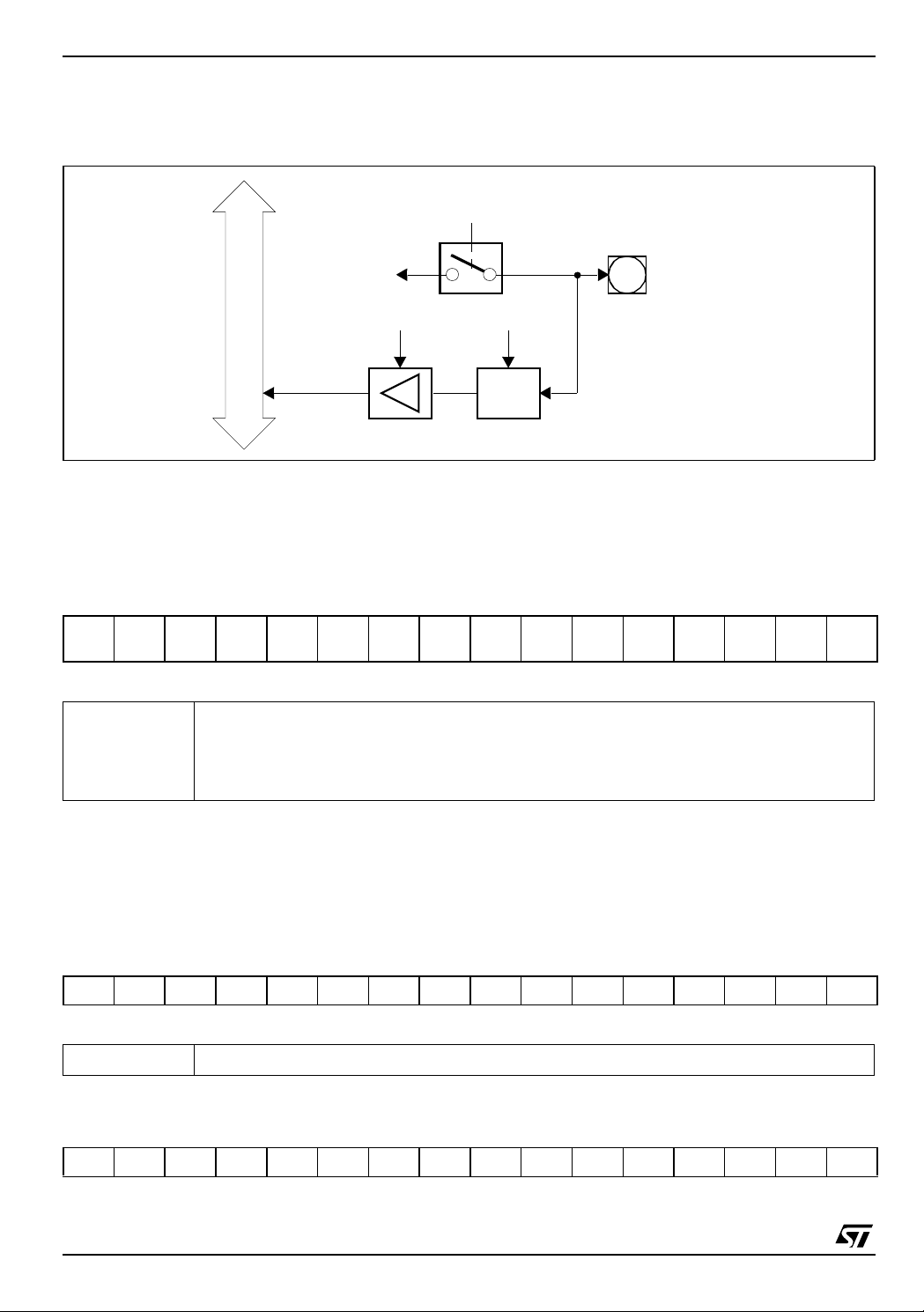
12 - PARALLEL PORTS ST10F269
Port 5 pins have a special port structure (see Figure 35), first because it is an input only port, and second
because the analog input channels are directly connected to the pins rather than to the input latches.
Figure 35 : Block Diagram of a Port 5 Pin
Channel
Select
Analog
to Sample + Hold
Circuit
Switch
P5.y/ANy
Read Port P5.y
Internal Bus
Read
Buffer
Clock
Input
Latch
y = 15...0
12.8.2 - Port 5 Schmitt Trigger Analog Inputs
A Schmitt trigger protection can be ac tivated on each pin of Port 5 by setting the dedicated bit of register
P5DIDIS.
P5DIDIS (FFA4h / D2h) SFR Reset Value: 0000h
1514131211109876543210
P5DI
P5DI
P5DI
P5DI
P5DI
P5DI
P5DI
P5DI
P5DI
P5DI
P5DI
P5DI
DIS.15
DIS.14
DIS.13
DIS.12
DIS.11
DIS.10
RW RW RW RW RW RW RW RW RW RW RW RW RW RW RW RW
DIS.9
DIS.8
DIS.7
DIS.6
DIS.5
DIS.4
P5DI
DIS.3
P5DI
DIS.2
P5DI
DIS.1
P5DI
DIS.0
P5DIDIS.y Port 5 Digital Disable Register Bit y
P5DIDIS.y = 0: Port line P5.y digital input is enabled (Schmitt trigger enabled)
P5DIDIS.y = 1: Port line P5.y digital input is disabled (Schmitt trigger disabled,
necessary for input leakage current reduction)
12.9 - Port 6
If this 8-bit por t is used for general purpose I/O, the direction of eac h line can be configured via the
corresponding direction regi ster DP6. Each por t line can be switched into push/ pull or op en drain mode
via the open drain control register ODP6.
P6 (FFCCh / E6h) SFR Reset Value: --00h
1514131211109876543210
- - - - - - - - P6.7 P6.6 P6.5 P6.4 P6.3 P6.2 P6.1 P6.0
RW RW RW RW RW RW RW RW
P6.y Port Data Register P6 Bit y
DP6 (FFCEH / E7H) SFR Reset Value: --00h
1514131211109876543210
--------DP6.7DP6.6DP6.5DP6.4DP6.3DP6.2DP6.1DP6.0
RW RW RW RW RW RW RW RW
82/184

ST10F269 12 - PARALLEL PORTS
DP6.y Port Direction Register DP6 Bit y
DP6.y = 0: Port line P6.y is an input (high impedance)
DP6.y = 1: Port line P6.y is an output
ODP6 (F1CEH / E7H) ESFR Reset Value: --00h
1514131211109876543210
--------ODP6.7ODP6.6ODP6.5ODP6.4ODP6.3ODP6.2ODP6.1ODP6.0
RW RW RW RW RW RW RW RW
ODP6.y Port 6 Open Drain Control Register Bit y
ODP6.y = 0: Port line P6.y output driver in push-pull mode
ODP6.y = 1: Port line P6.y output driver in open drain mode
12.9.1 - Alternate Functions of Port 6
A programmable number of chip select signals (CS4
(BUSCON4...BUSCON0) can be output on 5 pins of Port 6.
The number of chip select signa ls is selected via PORT0 during reset . The selected value can be read
from bit-field CSSEL in register RP0H (read only) in order to check the configuration during run time.
The Table 23 summari zes the alternat e functions of Port 6 depending on the number of selected chip
select lines (coded via bit-field CSSEL).
Table 23 : Port 6 Alternat e Funct ions
...CS0) derived from the bus control registers
Port 6
P6.0
P6.1
P6.2
P6.3
P6.4
P6.5
P6.6
P6.7
Alternate Function
CSSEL = 10
General purpose I/O
General purpose I/O
General purpose I/O
General purpose I/O
General purpose I/O
HOLD
External hold request input
HLDA
Hold acknowledge output
BREQ
Bus request output
Alternate Function
CSSEL = 01
Chip select CS0
Chip select CS1
General purpose I/O
General purpose I/O
General purpose I/O
Figure 36 : Port 6 I/O and Alternate Functions
Alternate Function a)
Port 6
P6.7
P6.6
P6.5
P6.4
P6.3
P6.2
P6.1
P6.0
Alternate Function
CSSEL = 00
Chip select CS0
Chip select CS1
Chip select CS2
General purpose I/O
General purpose I/O
BREQ
HLDA
HOLD
CS4
CS3
CS2
CS1
CS0
Alternate Function
CSSEL = 11
Chip select CS0
Chip select CS1
Chip select CS2
Chip select CS3
Chip select CS4
General Purpose Input/Output
83/184

12 - PARALLEL PORTS ST10F269
The chip select lines of Port 6 have an internal
weak pull-up device. This device is switched on
alternate function (CS
this case.
during reset. This feature is implemented to drive
the chip select lines high during res et in order to
avoid multiple chip selection.
After reset the CS
function must be used, if
selected so. In this case there is no possibility to
program any port latches before. Thus the
Note: The ope n drain output option can only be
selected via software earliest during the
initialization routine; at least signal CS0
will be in push/pull output driver mode
directly afte r r ese t.
Figure 37 : Block Diagram of Port 6 Pins with an Alternate Output Function
Write ODP6.y
Open Drain
Latch
Read ODP6.y
Write DP6.y
Direction
Latch
"0"
"1"
1
0
MUX
1
0
MUX
MUX
) is selected automatically in
Read DP6.y
MUX
Alternate
Function
Enable
Alternate
Data
Output
1
0
1
0
MUX
Clock
Input
Latch
Output
Buffer
P6.y
y = (0...4, 6, 7)
Internal Bus
Write DP6.y
Port Output
Latch
Read P6.y
84/184

ST10F269 12 - PARALLEL PORTS
Figure 38 : Block Diagram of Pin P6.5 (HOLD)
Write ODP6.5
Open Drain
Latch
Read ODP6.5
Write DP6.5
Direction
Latch
Read DP6.5
Internal Bus
Write P6.5
Port Output
Latch
Read P6.5
Alternate Data Input
MUX
Output
Buffer
1
0
Clock
Input
Latch
P6.5/HOLD
85/184

12 - PARALLEL PORTS ST10F269
12.10 - Port 7
If this 8-bit por t is used for general purpose I/O, the direction of eac h line can be configured via the
corresponding direction register DP 7. Each port line can be switched into pu sh-pull or open d rain mode
via the open drain control register ODP7.
P7 (FFD0h / E8h) SFR Reset Value: --00h
1514131211109876543210
- - - - - - - - P7.7 P7.6 P7.5 P7.4 P7.3 P7.2 P7.1 P7.0
RW RW RW RW RW RW RW RW
P7.y Port Data Register P7 Bit y
DP7 (FFD2h / E9h) SFR Reset Value: --00h
1514131211109876543210
--------DP7.7DP7.6DP7.5DP7.4DP7.3DP7.2DP7.1DP7.0
RW RW RW RW RW RW RW RW
DP7.y Port Direction Register DP7 Bit y
DP7.y = 0: Port line P7.y is an input (high impedance)
DP7.y = 1: Port line P7.y is an output
ODP7 (F1D2h / E9h) ESFR Reset Value: --00h
1514131211109876543210
--------ODP7.7ODP7.6ODP7.5ODP7.4ODP7.3ODP7.2ODP7.1ODP7.0
RW RW RW RW RW RW RW RW
ODP7.y Po rt 7 Open Drain Control Register Bit y
ODP7.y = 0: Port line P7.y output driver in push-pull mode
ODP7.y = 1: Port line P7.y output driver in open drain mode
86/184

ST10F269 12 - PARALLEL PORTS
12.10.1 - Alternate Functions of Port 7
The upper 4 lines of Port 7 (P7.7...P7.4) serve as
capture inputs or compare outputs
(CC31IO...CC28IO) for the CAPCOM2 unit.
The usage of the por t lines by the CAPCO M unit,
its ac cessibility v ia software a nd the pr ecautions
are the same as described for the Port 2 lines.
As all other capture inputs, the capture input
function of pins P7.7...P7.4 can also be used as
external interrupt inputs (200ns sample rate at
40MHz CPU clock on PQFP144 devices and
250ns sample rate at 32MHz CPU clock on
TQFP14 4 d evices).
The lower 4 lines of Port 7 (P7.3...P7.0) serve as
outputs from the PWM module
(POUT3...POUT0).
At these pins the value of the respective port
output latch is EXORed with the value of the PWM
output rather than ANDed, as the other pins do.
This allows to use the alternate output value either
as it is (port latch holds a ‘0’) or to invert its level at
the pin (port latch holds a ‘1’).
Note that the PWM outputs must be enabled via
the respective PENx bit in PWMCON1.
The Table 24 summar izes the alternate functions
of Port 7.
Table 24 : Port 7 Alternat e Funct ions
Port 7 Alternate Function
P7.0
P7.1
P7.2
P7.3
P7.4
P7.5
P7.6
P7.7
POUT0 PWM mode channel 0 output
POUT1 PWM mode channel 1 output
POUT2 PWM mode channel 2 output
POUT3 PWM mode channel 3 output
CC28IO Capture input / com pare outpu t channel 28
CC29IO Capture input / com pare outpu t channel 29
CC30IO Capture input / com pare outpu t channel 30
CC31IO Capture input / com pare outpu t channel 31
Figure 39 : Port 7 I/O and Alternate Functions
Port 7
General Purpose Input/Output
P7.7
P7.6
P7.5
P7.4
P7.3
P7.2
P7.1
P7.0
CC31IO
CC30IO
CC29IO
CC28IO
POUT3
POUT2
POUT1
POUT0
Alternate Function
87/184

12 - PARALLEL PORTS ST10F269
The structure of Port 7 differs in the way t heoutput
latches are connected to the internal bus and to
the pin driver. Pins P7.3...P7.0 (POUT3...POUT0)
Figure 40 : Block Diagram of Port 7 Pins P7.3...P7.0
Write ODP7.y
Open Drain
Latch
Read ODP7.y
Write DP7.y
Direction
Latch
EXOR the alternate data output with the port latch
output, which allows to use the alternate data
directly or inverted at the pin driver.
Internal Bus
Read DP7.y
Write DP7.y
Port Output
Latch
Read P7.y
MUX
Port Data
Output
1
0
Alternate
Data
Output
=1
EXOR
Clock
Input
Latch
Output
Buffer
P7.y/POUTy
y = 0...3
88/184

ST10F269 12 - PARALLEL PORTS
Figure 41 : Block Diagram of Port 7 Pins P7.7...P7.4
Write ODP7.y
Open Drain
Latch
Read ODP7.y
Write DP7.y
Direction
Latch
Internal Bus
Alternate
Data
Output
Write Port P7.y
Compare Trigger
Read DP7.y
1
MUX
0
Read P7.y
≥ 1
Output
Latch
Alte rnate Latc h
Data Input
MUX
P7.y
Output
Buffer
Clock
1
0
Alternate Pin
Data Input
Input
Latch
y = (4...7)
z = (28...31)
CCzIO
89/184

12 - PARALLEL PORTS ST10F269
12.11 - Port 8
If this 8-bit port is used for general purpose I/O,
the direction of each line can be configured via the
corresponding direction register DP8. Each port
line can be switched into push/pull or open drain
mode via the open drain control register ODP8.
P8 (FFD4h / EAh) SFR Reset Value: --00h
1514131211109876543210
- - - - - - - - P8.7 P8.6 P8.5 P8.4 P8.3 P8.2 P8.1 P8.0
RW RW RW RW RW RW RW RW
P8.y Port Data Register P8 Bit y
DP8 (FFD6h / EBh) SFR Reset Value: --00h
1514131211109876543210
--------DP8.7DP8.6DP8.5DP8.4DP8.3DP8.2DP8.1DP8.0
RW RW RW RW RW RW RW RW
DP8.y Port Direction Register DP8 Bit y
DP8.y = 0: Port line P8.y is an input (high impedance)
DP8.y = 1: Port line P8.y is an output
ODP8 (F1D6h / EBh) ESFR Reset Value: --00h
1514131211109876543210
--------ODP8.7ODP8.6ODP8.5ODP8.4ODP8.3ODP8.2ODP8.1ODP8.0
RW RW RW RW RW RW RW RW
ODP8.y Po rt 8 Open Drain Control Register Bit y
ODP8.y = 0: Port line P8.y output driver in push-pull mode
ODP8.y = 1: Port line P8.y output driver in open drain mode
90/184

ST10F269 12 - PARALLEL PORTS
12.11.1 - Alternate Functions of Port 8
The 8 lines of Port 8 serve as capture inputs or as
compare outputs (CC23IO...CC16IO) for the
CAPCOM2 unit.
The usage of the por t lines by the CAPCO M unit,
its ac cessibility v ia software a nd the pr ecautions
are the same as described for the Port 2 lines.
As all other capture inputs, the capture input
function of pins P8.7...P8.0 can also be used as
external interrupt inputs (200ns sample rate at
40MHz CPU clock on PQFP144 devices and
250ns sample rate at 32MHz CPU clock on
TQFP14 4 d evices).
The Table 25 summar izes the alternate functions
of Port 8.
Table 25 : Port 8 Alternat e Funct ions
Port 7 Alternate Function
P8.0
P8.1
P8.2
P8.3
P8.4
P8.5
P8.6
P8.7
CC16IO Capture input / compare output channel 16
CC17IO Capture input / compare output channel 17
CC18IO Capture input / compare output channel 18
CC19IO Capture input / compare output channel 19
CC20IO Capture input / compare output channel 20
CC21IO Capture input / compare output channel 21
CC22IO Capture input / compare output channel 22
CC23IO Capture input / compare output channel 23
Figure 42 : Port 8 I/O and Alternate Functions
Port 8
P8.7
P8.6
P8.5
P8.4
P8.3
P8.2
P8.1
P8.0
CC23IO
CC22IO
CC21IO
CC20IO
CC19IO
CC18IO
CC17IO
CC16IO
Alternate FunctionGeneral Purpose Input / Output
91/184
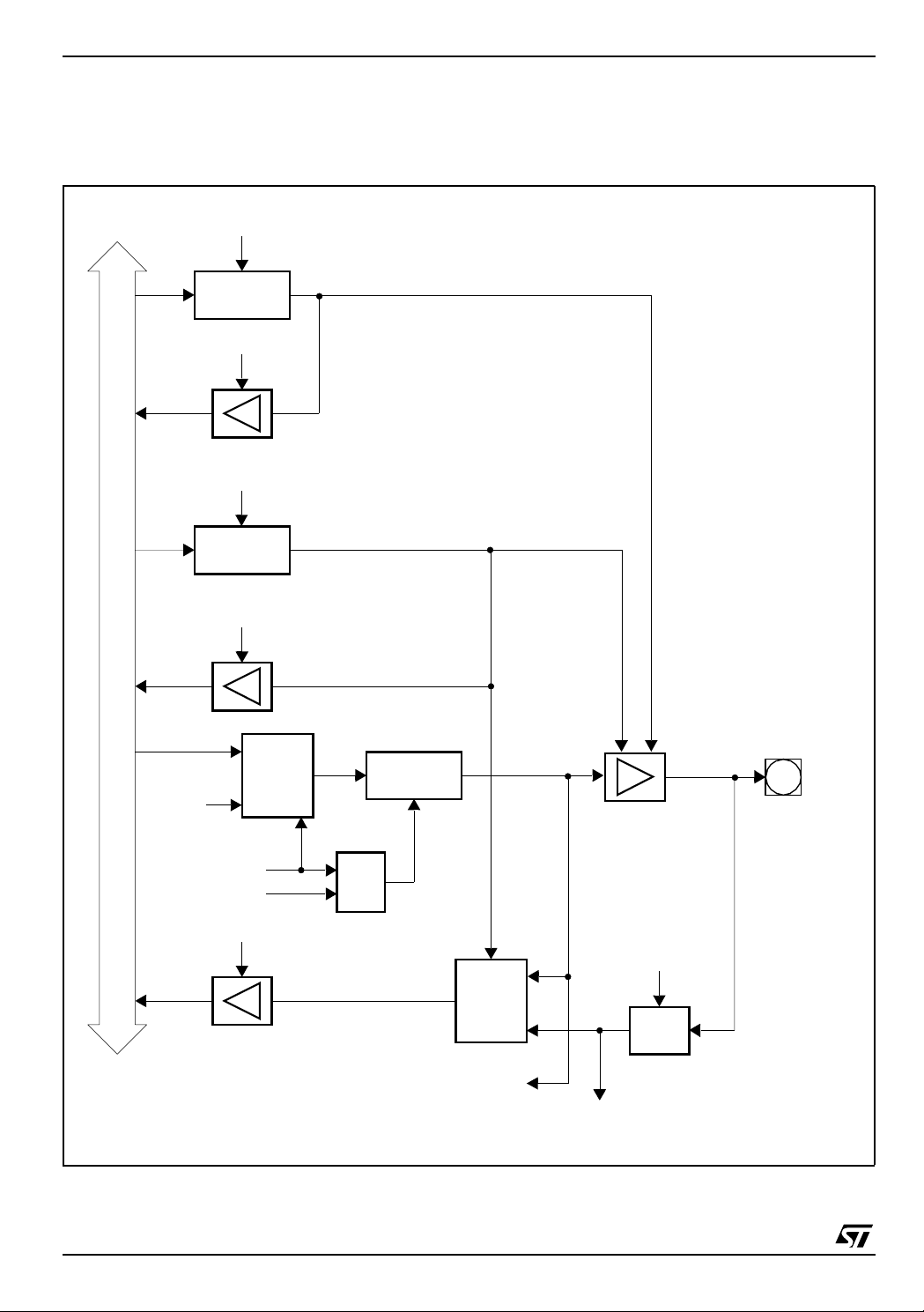
12 - PARALLEL PORTS ST10F269
The structure of Port 8 differs in the way the output
latches are connected to the internal bus and to
the pin driver (see Figure 43). Pins P8.7...P8.0
Figure 43 : Block Diagram of Port 8 Pins P8.7...P8.0
Write ODP8.y
Open Drain
Latch
Read ODP8.y
Write DP8.y
Direction
Latch
(CC23IO...CC16IO) combine internal bus data
and alternate data output before the port latch
input, as do the Port 2 pins.
Inter n a l Bus
Alternate
Data
Output
Write Port P8.y
Compare Trigger
Read DP8.y
1
MUX
0
Read P8.y
≥ 1
Output
Latch
Alternate Latch
Data Input
MUX
P8.y
Output
Buffer
Clock
1
0
Alternate Pin
Data Input
Input
Latch
y = (7...0)
z = (16...23)
CCzIO
92/184

ST10F269 13 - A/D CONVERTER
13 - A/D CONVERTER
A 10-bit A/D convert er with 16 multiplexed input
channels and a sample and hold circuit is
integrated on-chip. The sample time (for loading
the capacitors) and the conversion time is
programmable and can be adjusted to the
external circuitry.
To remove high frequency c omponents from the
analog input signal, a low-pass filter must be c onnected at the ADC input.
Overrun error detection / protection is cont rolled
by the ADDAT register. Either an interrupt request
is generated when the result of a previous
conversion has not been read from the result
register at the time the next conversion is
complete, or the next conversion is suspended
until the previous result has been read. For
applications which require less than 16 analog
input channels, the remaining channel inpu ts can
be used as digital input port pins. The A/D
converter of the ST10F269 supports different
conversion modes:
– Single channel single conversi on : the anal og
level of the selected channel is sam pled once
and converted. The resul t of the conversion is
stored in the ADDAT register.
– Single channel continuous conversion: the
analog level of the selected channel is repeatedly sampled and converted. The result of the conversion is stored in the ADDAT register.
converted. After each conversion the result is
stored in the ADDAT register. The data can be
transferred to the RAM by interrupt software
management or using the powerful Peripheral
Event Controller (PEC) data transfer.
– Auto scan continuous conversion: the analog
level of the selected channels are repeatedly
sampled and converted. The result of the conversion is stored in the ADDAT register. The
data can be transferred to the RA M by interrupt
software management or using the PEC data
transfer.
– Wait for ADDAT read mode: when using con-
tinuous modes, in order to avoid to overwrite
the result of the current conversion by the next
one, the ADWR bit of ADCON control register
must be activated. Then, until the ADDAT register is read, the new result is stored in a temporary buffer and the conversion is on hold.
– Channel injection mode: when using
continuous modes, a selected channe l can be
converted in between without changing the
current operating mode. The 10-bit data of the
conversion are stored in ADRES field of
ADDAT2. The current continuous mode remains
active after the single conversion is completed
– Auto scan single conversion: the analog level
of the selected channels are sampl ed onc e and
Table 26 : ADC Sample Clock and Conversion Clock (PQFP144 devices)
Conversion Clock t
ADCTC
TCL1 = 1/2 x f
00 TCL x 24 0.3µs00 t
01 Reserved, do not use Reserved 01 t
10 TCL x 96 1.2 µs10t
11 TCL x 48 0.6 µs11t
Notes: 1. Section 21.4.5 -: Direct Drive for TCL definition.
= TCL x 24
2. t
CC
XTAL
CC
ADSTC
At f
= 40MHz tSC =At f
CPU
Sample Clock t
CC
x 2
CC
x 4
CC
x 8
CC
SC
CPU
0.3µs
0.6µs
1.2µs
2.4µs
= 40MHz
2
2
2
2
93/184

13 - A/D CONVERTER ST10F269
Table 27 : ADC Sample Clock and Conversion Clock (TQFP144 devices)
ADCON 15/14
ADCTC
Conversion Clock t
TCL1 = 1/2 x f
XTAL
CC
At f
= 32MHz tSC =At f
CPU
ADCON 13/12
ADSTC
00 TCL x 24 0.375µs00 t
01 Reserved, do not use Reserved 01 t
10 TCL x 96 1.5 µs10t
11 TCL x 48 0.75 µs11t
Notes: 1. Section 21.4.5 -: Direct Drive for TCL definition.
2. t
CC
= TCL x 24
Sample Clock t
CC
x 2
CC
x 4
CC
x 8
CC
SC
= 32MHz
CPU
0.375µs
0.75µs
1.50µs
3.00µs
2
2
2
2
94/184

ST10F269 14 - SERIAL CHANNELS
14 - SERIAL CHANNELS
Serial communication with other microcontrollers,
microprocessors, terminals or external peripheral
components is provided by two serial interfaces:
the asynchronous / synchronous serial channel
(ASCO) and the high-speed synchronous serial
channel (SSC). Two dedicated Baud rate
generators set up all standard Baud rates without
the requirement of oscillator tuning. For
transmission, reception and erroneous recept ion,
3 separate interrupt vectors are provided for eac h
serial channel.
14.1 - Asynchronous / Synchronous Serial Interface (ASCO)
The asynchronous / synchronous serial interface
(ASCO) provides serial communication between
the ST10F269 and other microcontrollers,
microprocessors or external peripherals.
A set of registers is used to configure and to
control the ASCO serial interface:
– P3, DP3, ODP3 for pin configuration
– SOBG for Baud rate generator
– SOTBUF for transmit buffer
– SOTIC for transmit interrupt control
– SOTBIC for transmit buffer interrupt control
– SOCON for control
– SORBUF for receive buffer (read only)
– SORIC for receive interrupt control
– SOEIC for error interrupt control
14.1.1 - ASCO in Asynchronous Mode
In asynchronous mode, 8 or 9-bit data transfer,
parity generation an d the number of stop bi t can
be selected. Parity framing and overrun error
detection is provided to increase the reliability of
data transfers. Transmission and reception of data
is double-buffered. Full-duplex communication up
to 1.25M Bauds (at 40MHz f
devices) and up to 1MBaud (at 32MHz f
TQFP144 devices) is suppor ted in this mode.
Figure 44 : Asynchronous Mode of Ser ial Channel ASC0
Reload Register
on PQFP144
CPU
CPU
on
CPU
Clock
Input
RXD0/P3.11
Pin
2
S0R
S0REN
S0FEN
S0PEN
S0OEN
S0LB
0
1
SamplingMUX
Baud Rate Timer
S0M S0STP S0FE S0OE
Clock
Serial Port Control
Shift Clock
Receive Shift
Register
Receive Buffer
Registe r S0 RBUF
Internal Bus
Register S0TBUF
16
S0PE
Transmit Shift
Register
Transmit B uf fer
S0RIR
S0TIR
S0EIR
Pin
TXD0 / P3.10
Output
Receive In t errupt
Request
Transmit Interrupt
Request
Error Interrupt
Request
95/184

14 - SERIAL CHANNELS ST10F269
Asynchronous Mode Baud rates
For asynchronous operation, the Baud rate
generator provides a clock with 16 tim es the rate
of the established Baud rate. Every received bit is
sampled at the 7th, 8th and 9th cycle of this clock.
The Baud rate for asynchronous operation of
B
=
Async
S0BRL = (
16 x [2 + (S0BRS)] x [(S0BRL) + 1]
16 x [2 + (S0BRS)] x B
f
f
CPU
CPU
Async
serial channel ASC0 and the required reload
value for a given Baud rate can be determined by
the following formulas:
Using the above equation, the maximum Baud
rate can be calculated for any given clock speed.
(S0BRL) represents the content of the reload
register, taken as unsigned 13-bit integer,
(S0BRS) represents the value of bit S0BRS (‘0’ or
‘1’), taken as integer.
Baud rate versus reload register value (SOBRS=0
and SOBRS=1) is described in Table 28. and
Table 29
Table 28 : Commonly Used Baud Rates by Reload Value and Deviation Errors (PQFP144 devices)
S0BRS = ‘0’, f
Baud Rate (Baud) Deviation Error
1 250 000 0.0% / 0.0% 0000 / 0000 833 333 0.0% / 0.0% 0000 / 0000
112 000 +1.5% / -7.0% 000A / 000B 112 000 +6.3% / -7.0% 0006 / 0007
56 000 +1.5% / -3.0% 0015 / 0016 56 000 +6.3% / -0.8% 000D / 000E
38 400 +1.7% / -1.4% 001F / 0020 38 400 +3.3% / -1.4% 0014 / 0015
19 200 +0.2% / -1.4% 0040 / 0041 19 200 +0.9% / -1.4% 002A / 002B
9 600 +0.2% / -0.6% 0081 / 0082 9 600 +0.9% / -0.2% 0055 / 0056
4 800 +0.2% / -0.2% 0103 / 0104 4 800 +0.4% / -0.2% 00AC / 00AD
2 400 +0.2% / -0.0% 0207 / 0208 2 400 +0.1% / -0.2% 015A / 015B
1 200 0.1% / 0.0% 0410 / 0411 1 200 +0.1% / -0.1% 02B5 / 02B6
600 0.0% / 0.0% 0822 / 0823 600 +0.1% / -0.0% 056B / 056C
300 0.0% / 0.0% 1045 / 1046 300 0.0% / 0.0% 0AD8 / 0AD9
153 0.0% / 0.0% 1FE8 / 1FE9 102 0.0% / 0.0% 1FE8 / 1FE9
= 40MHz S0BRS = ‘1’, f
CPU
Reload Value
(hexa)
Baud Rate (Baud) Deviation Error
CPU
= 40MHz
Reload Value
(hexa)
) - 1
Note: The deviation errors given in the Table 28 are rounded. To avoid deviation errors use a Baud rate
crystal (providing a multiple of the ASC0/SSC sampling frequency).
96/184
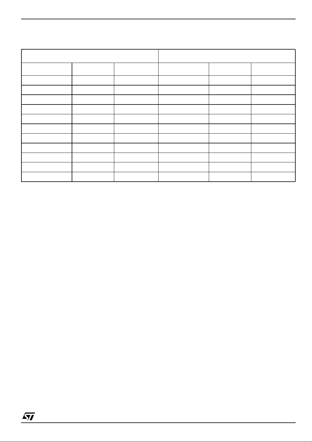
ST10F269 14 - SERIAL CHANNELS
Table 29 : Commonly Used Baud Rates by Reload Value and Deviation Errors (TQFP144 devices)
S0BRS = ‘0’, f
Baud Rate (Baud) Deviation Error Reload Value Baud Rate (Baud) Deviation Error Reload Value
1000 000 ±0.0% 0000h 666 667 ±0.0% 0000h
56000 +5.0% / -0.8% 0010h / 001h 56000 +8.2% / -0.8% 000Ah / 000Bh
38400 +0.2% / -3.5% 0019h / 0020h 38400 +2.1% / -3.5% 0010h / 0011h
19200 +0.2% / -1.7% 0033h / 0034h 19200 +2.1% / -0.8% 0021h / 0022h
9600 +0.2% / -0.8% 0067h/ 0068h 9600 +0.6% / -0.8% 0044h / 0045h
4800 +0.5% / -0.3% 00CFh / 00CEh 4800 +0.6% / -0.1% 0089h / 008Ah
2400 +0.2% / -0.1% 019Fh / 01A0h 2400 +0.3% / -0.1% 0114h / 0115h
1200 +0.1% / -0.1% 0340h / 0341h 1200 +0.1% / -0.1% 022Ah / 022Bh
600 +0.1% / -0.1% 0681h / 0682h 600 +0.1% / -0.1% 0456h / 0457h
95 +0.1% / -0.1% 291Dh / 291Eh 75 +0.1% / 0.1% 22B7h / 22B8h
= 32MHz S0BRS = ‘1’, f
CPU
63 +0.1% / -0.1% 2955h / 2956h
CPU
= 32MHz
Note: The deviation errors given in the Table 29 are rounded. To avoid deviation errors use a Baud rate
crystal (providing a multiple of the ASC0/SSC sampling frequency).
97/184

14 - SERIAL CHANNELS ST10F269
14.1.2 - ASCO in Synchronous Mode
In synchronous mode, data are transmitted or received synchronously to a shift clock which is generated
by the ST10F269. Half-duplex communication up to 5M Baud (at 40MHz f
possible in this mode.
Figure 45 : Synchronous Mode of Serial Channel ASC0
Reload Register
) or 4M Baud (at 32MHz) is
CPU
CPU
Clock
Output
TDX0/P3.10
Pin
Input/Output
RXD0/P3.11
Pin
Receive
Transmit
S0R
0
1
S0REN
S0OEN
S0LB
MUX
2
Baud Rate Timer
S0M = 000B S0OE
Clock
Serial Port Control
Shift Clock
Receive S h ift
Register
Receive Buffer
Register S0RBUF
Internal Bus
4
Transmit Shift
Register
Transmit Buffer
Register S0TBUF
S0RIR
S0TIR
S0EIR
Receive Inte r r upt
Request
Transmit Interrupt
Request
Error Interrupt
Request
98/184

ST10F269 14 - SERIAL CHANNELS
Synchronous Mode Baud Rates
f
For synchronous operation, the Baud rate
generator provides a clock with 4 times the rate of
the established Baud rate. The Baud rate for
B
Sync
=
4 x [2 + (S0BRS)] x [(S0BRL) + 1]
synchronous operation of serial channel ASC0
can be determined by the following formula:
(S0BRL) represents the content of the reload
register, taken as unsigned 13-bit integers,
(S0BRS) represents the value of bit S0BRS (‘0’ or
‘1’), taken as integer.
S0BRL = (
4 x [2 + (S0BRS)] x B
Using the above equation, the maximum Baud
rate can be calculated for any clock speed as
given in Table 30.and Table 31
Table 30 : Commonly Used Baud Rates by Reload Value and Deviation Errors (PQFP144 devices)
CPU
f
CPU
) - 1
Sync
S0BRS = ‘0’, f
Baud Rate (Baud) Deviation Error
5 000 000 0.0% / 0.0% 0000 / 0000 3 333 333 0.0% / 0.0% 0000 / 0000
112 000 +1.5% / -0.8% 002B / 002C 112 000 +2.6% / -0.8% 001C / 001D
56 000 +0.3% / -0.8% 0058 / 0059 56 000 +0.9% / -0.8% 003A / 003B
38 400 +0.2% / -0.6% 0081 / 0082 38 400 +0.9% / -0.2% 0055 / 0056
19 200 +0.2% / -0.2% 0103 / 0104 19 200 +0.4% / -0.2% 00AC / 00AD
9 600 +0.2% / -0.0% 0207 / 0208 9 600 +0.1% / -0.2% 015A / 015B
4 800 +0.1% / -0.0% 0410 / 0411 4 800 +0.1% / -0.1% 02B5 / 02B6
2 400 0.0% / 0.0% 0822 / 0823 2 400 +0.1% / -0.0% 056B / 056C
1 200 0.0% / 0.0% 1045 / 1046 1 200 0.0% / 0.0% 0AD8 / 0AD9
900 0.0% / 0.0% 15B2 / 15B3 600 0.0% / 0.0% 15B2 / 15B3
612 0.0% / 0.0% 1FE8 / 1FE9 407 0.0% / 0.0% 1FFD / 1FFE
= 40MHz S0BRS = ‘1’, f
CPU
Reload Value
(hexa)
Baud Rate (Baud) Deviation Error
CPU
= 40MHz
Reload Value
(hexa)
Note: The deviation errors given in the Table 30 are rounded. To avoid deviation errors use a Baud rate
crystal (providing a multiple of the ASC0/SSC sampling frequency)
99/184

14 - SERIAL CHANNELS ST10F269
Table 31 : Commonly Used Baud Rates by Reload Value and Deviation Errors (TQFP144 devices)
S0BRS = ‘0’, f
Baud Rate (Baud) Deviation Error Reload Value Baud Rate (Baud) Deviation Error Reload Value
4 000 000 ±0.0% 0000h 2 666 667 ±0.0% 0000h
224 000 +5.0% / -0.8% 0011h / 0012h 224 000 +8.2% / -0.8% 000Bh / 000Ch
112 000 +2.0% / -0.8% 0023h / 0024h 112 000 +3.5% / -0.8% 0017h / 0018h
56 000 +0.6% / -0.8% 0046h / 0047h 56 000 +1.3% / -0.8% 002Fh / 0030h
38 400 +0.2% / -0.85% 0077h / 0078h 38 400 +0.6% / -0.8% 0044h / 0045h
19 200 +0.2% / -0.3% 00BFh / 00C0h 19 200 +0.6% / -0.1% 008Ah / 008Bh
9 600 +0.2% / -0.1% 01A0h/ 01A1h 9 600 +0.3% / -0.1% 0115h / 0116h
4 800 +0.0% / -0.1% 0340h / 0341h 4 800 +0.1% / -0.1% 022Bh / 022Ch
2 400 +0.0% / -0.0% 0682h / 0683h 2 400 +0.0% / -0.1% 0456h / 0457h
1 200 +0.0% / -0.0% 004h / 0D05h 1 200 +0.0% / -0.0% 08ACh / 08ADh
600 +0.0% / -0.0% 1A0Ah / 1A0Bh 600 +0.0% / -0.0% 115Bh / 115C7h
490 +0.0% / -0.0% 1FE2h / 1FE3h 320 +0.2% 1FFFh
= 32MHz S0BRS = ‘1’, f
CPU
CPU
= 32MHz
Note: The deviation errors given in the Table 31 are rounded. To avoid deviation errors use a Baud rate
crystal (providing a multiple of the ASC0/SSC sampling frequency)
100/184
 Loading...