

SPC564A74B4, SPC564A74L7,
SPC564A80B4, SPC564A80L7
32-bit MCU family built on the embedded Power Architecture
Features
■ 150 MHz e200z4 Power Architecture
– Variable length instruction encoding (VLE)
– Superscalar architecture with 2 execution
units
– Up to 2 integer or floating point instructions
per cycle
– Up to 4 multiply and accumulate operations
per cycle
■ Memory organization
– 4 MB on-chip flash memory with ECC and
Read While Write (RWW)
– 192 KB on-chip RAM with standby
functionality (32 KB) and ECC
– 8 KB instruction cache (with line locking),
configurable as 2- or 4-way
– 14 + 3 KB eTPU code and data RAM
–5× 4 crossbar switch (XBAR)
– 24-entry MMU
– External Bus Interface (EBI) with slave and
master port
■ Fail Safe Protection
– 16-entry Memory Protection Unit (MPU)
– CRC unit with 3 sub-modules
– Junction temperature sensor
■ Interrupts
– Configurable interrupt controller (with NMI)
– 64-channel DMA
■ Serial channels
–3× eSCI
–3× DSPI (2 of which support downstream
Micro Second Channel [MSC])
Table 1. Device summary
Memory Flash
size
Package LQFP176 Package: LBGA208 Package: PBGA324 KGD
®
core
®
LBGA208
–3× FlexCAN with 64 messages each
–1× FlexRay module (V2.1) up to 10 Mbit/s
with dual or single channel and 128
message objects and ECC
■ 1 × eMIOS
■ 1 × eTPU2 (second generation eTPU)
■ 2 enhanced queued analog-to-digital
converters (eQADCs)
■ On-chip CAN/SCI/FlexRay Bootstrap loader
with Boot Assist Module (BAM)
■ Nexus: Class 3+ for core; Class 1 for the eTPU
■ JTAG (5-pin)
■ Development Trigger Semaphore (DTS)
■ Clock generation
– On-chip 4–40 MHz main oscillator
– On-chip FMPLL (frequency-modulated
phase-locked loop)
■ Up to 120 general purpose I/O lines
■ Power reduction mode: slow, stop and stand-
by modes
■ Flexible supply scheme
– 5 V single supply with external ballast
– Multiple external supply: 5 V, 3.3 V and
1.2 V
■ Designed for LQFP176, LBGA208, PBGA324
and Known Good Die (KGD)
Part number
PBGA324
LQFP176
4MB SPC564A80L7 - SPC564A80B4 -
3MB SPC564A74L7 - SPC564A74B4 -
March 2012 Doc ID 15399 Rev 8 1/157
www.st.com
1

Contents SPC564A74B4, SPC564A74L7, SPC564A80B4, SPC564A80L7
Contents
1 Introduction . . . . . . . . . . . . . . . . . . . . . . . . . . . . . . . . . . . . . . . . . . . . . . . . 8
1.1 Document Overview . . . . . . . . . . . . . . . . . . . . . . . . . . . . . . . . . . . . . . . . . . 8
1.2 Description . . . . . . . . . . . . . . . . . . . . . . . . . . . . . . . . . . . . . . . . . . . . . . . . . 8
1.3 Device comparison . . . . . . . . . . . . . . . . . . . . . . . . . . . . . . . . . . . . . . . . . . . 9
1.4 SPC564A80 feature list . . . . . . . . . . . . . . . . . . . . . . . . . . . . . . . . . . . . . . 11
1.5 Feature details . . . . . . . . . . . . . . . . . . . . . . . . . . . . . . . . . . . . . . . . . . . . . 13
1.5.1 e200z4 core . . . . . . . . . . . . . . . . . . . . . . . . . . . . . . . . . . . . . . . . . . . . . . 13
1.5.2 Crossbar Switch (XBAR) . . . . . . . . . . . . . . . . . . . . . . . . . . . . . . . . . . . . 13
1.5.3 eDMA . . . . . . . . . . . . . . . . . . . . . . . . . . . . . . . . . . . . . . . . . . . . . . . . . . . 14
1.5.4 Interrupt controller . . . . . . . . . . . . . . . . . . . . . . . . . . . . . . . . . . . . . . . . . 14
1.5.5 Memory protection unit (MPU) . . . . . . . . . . . . . . . . . . . . . . . . . . . . . . . . 15
1.5.6 FMPLL . . . . . . . . . . . . . . . . . . . . . . . . . . . . . . . . . . . . . . . . . . . . . . . . . . 16
1.5.7 SIU . . . . . . . . . . . . . . . . . . . . . . . . . . . . . . . . . . . . . . . . . . . . . . . . . . . . . 16
1.5.8 Flash memory . . . . . . . . . . . . . . . . . . . . . . . . . . . . . . . . . . . . . . . . . . . . 17
1.5.9 BAM . . . . . . . . . . . . . . . . . . . . . . . . . . . . . . . . . . . . . . . . . . . . . . . . . . . . 18
1.5.10 eMIOS . . . . . . . . . . . . . . . . . . . . . . . . . . . . . . . . . . . . . . . . . . . . . . . . . . 19
1.5.11 eTPU2 . . . . . . . . . . . . . . . . . . . . . . . . . . . . . . . . . . . . . . . . . . . . . . . . . . 19
1.5.12 Reaction module . . . . . . . . . . . . . . . . . . . . . . . . . . . . . . . . . . . . . . . . . . 21
1.5.13 eQADC . . . . . . . . . . . . . . . . . . . . . . . . . . . . . . . . . . . . . . . . . . . . . . . . . 21
1.5.14 DSPI . . . . . . . . . . . . . . . . . . . . . . . . . . . . . . . . . . . . . . . . . . . . . . . . . . . 23
1.5.15 eSCI . . . . . . . . . . . . . . . . . . . . . . . . . . . . . . . . . . . . . . . . . . . . . . . . . . . . 24
1.5.16 FlexCAN . . . . . . . . . . . . . . . . . . . . . . . . . . . . . . . . . . . . . . . . . . . . . . . . . 24
1.5.17 FlexRay . . . . . . . . . . . . . . . . . . . . . . . . . . . . . . . . . . . . . . . . . . . . . . . . . 26
1.5.18 System timers . . . . . . . . . . . . . . . . . . . . . . . . . . . . . . . . . . . . . . . . . . . . 26
1.5.19 Software watchdog timer (SWT) . . . . . . . . . . . . . . . . . . . . . . . . . . . . . . 27
1.5.20 Cyclic redundancy check (CRC) module . . . . . . . . . . . . . . . . . . . . . . . . 27
1.5.21 Error correction status module (ECSM) . . . . . . . . . . . . . . . . . . . . . . . . . 27
1.5.22 External bus interface (EBI) . . . . . . . . . . . . . . . . . . . . . . . . . . . . . . . . . . 28
1.5.23 Calibration EBI . . . . . . . . . . . . . . . . . . . . . . . . . . . . . . . . . . . . . . . . . . . . 28
1.5.24 Power management controller (PMC) . . . . . . . . . . . . . . . . . . . . . . . . . . 29
1.5.25 Nexus port controller . . . . . . . . . . . . . . . . . . . . . . . . . . . . . . . . . . . . . . . 29
1.5.26 JTAG . . . . . . . . . . . . . . . . . . . . . . . . . . . . . . . . . . . . . . . . . . . . . . . . . . . 29
1.5.27 Development Trigger Semaphore (DTS) . . . . . . . . . . . . . . . . . . . . . . . . 29
1.6 SPC564A80 series architecture . . . . . . . . . . . . . . . . . . . . . . . . . . . . . . . . 30
2/157 Doc ID 15399 Rev 8

SPC564A74B4, SPC564A74L7, SPC564A80B4, SPC564A80L7 Contents
1.6.1 Block diagram . . . . . . . . . . . . . . . . . . . . . . . . . . . . . . . . . . . . . . . . . . . . 30
1.6.2 Block summary . . . . . . . . . . . . . . . . . . . . . . . . . . . . . . . . . . . . . . . . . . . 32
2 Pinout and signal description . . . . . . . . . . . . . . . . . . . . . . . . . . . . . . . . 34
2.1 LQFP176 pinout . . . . . . . . . . . . . . . . . . . . . . . . . . . . . . . . . . . . . . . . . . . . 35
2.2 LBGA208 ballmap . . . . . . . . . . . . . . . . . . . . . . . . . . . . . . . . . . . . . . . . . . 36
2.3 PBGA324 ballmap . . . . . . . . . . . . . . . . . . . . . . . . . . . . . . . . . . . . . . . . . . 37
2.4 Signal summary . . . . . . . . . . . . . . . . . . . . . . . . . . . . . . . . . . . . . . . . . . . . 41
2.5 Signal details . . . . . . . . . . . . . . . . . . . . . . . . . . . . . . . . . . . . . . . . . . . . . . 73
3 Electrical characteristics . . . . . . . . . . . . . . . . . . . . . . . . . . . . . . . . . . . . 81
3.1 Parameter classification . . . . . . . . . . . . . . . . . . . . . . . . . . . . . . . . . . . . . . 81
3.2 Maximum ratings . . . . . . . . . . . . . . . . . . . . . . . . . . . . . . . . . . . . . . . . . . . 82
3.3 Thermal characteristics . . . . . . . . . . . . . . . . . . . . . . . . . . . . . . . . . . . . . . 83
3.3.1 General notes for specifications at maximum junction temperature . . . 85
3.4 EMI (electromagnetic interference) characteristics . . . . . . . . . . . . . . . . . 88
3.5 Electrostatic discharge (ESD) characteristics . . . . . . . . . . . . . . . . . . . . . 88
3.6 Power management control (PMC) and power on reset (POR) electrical
specifications . . . . . . . . . . . . . . . . . . . . . . . . . . . . . . . . . . . . . . . . . . . . . . 89
3.6.1 Regulator Example . . . . . . . . . . . . . . . . . . . . . . . . . . . . . . . . . . . . . . . . 92
3.6.2 Recommended power transistors . . . . . . . . . . . . . . . . . . . . . . . . . . . . . 94
3.7 Power up/down sequencing . . . . . . . . . . . . . . . . . . . . . . . . . . . . . . . . . . . 94
3.8 DC electrical specifications . . . . . . . . . . . . . . . . . . . . . . . . . . . . . . . . . . . 95
3.9 I/O pad current specifications . . . . . . . . . . . . . . . . . . . . . . . . . . . . . . . . . 101
3.9.1 I/O pad V
3.9.2 LVDS pad specifications . . . . . . . . . . . . . . . . . . . . . . . . . . . . . . . . . . . 103
current specifications . . . . . . . . . . . . . . . . . . . . . . . . . . 102
RC33
3.10 Oscillator and PLLMRFM electrical characteristics . . . . . . . . . . . . . . . . 104
3.11 Temperature sensor electrical characteristics . . . . . . . . . . . . . . . . . . . . 106
3.12 eQADC electrical characteristics . . . . . . . . . . . . . . . . . . . . . . . . . . . . . . 106
3.13 Configuring SRAM wait states . . . . . . . . . . . . . . . . . . . . . . . . . . . . . . . . 109
3.14 Platform flash controller electrical characteristics . . . . . . . . . . . . . . . . . 109
3.15 Flash memory electrical characteristics . . . . . . . . . . . . . . . . . . . . . . . . . 109
3.16 AC specifications . . . . . . . . . . . . . . . . . . . . . . . . . . . . . . . . . . . . . . . . . . 111
3.16.1 Pad AC specifications . . . . . . . . . . . . . . . . . . . . . . . . . . . . . . . . . . . . . 111
3.17 AC timing . . . . . . . . . . . . . . . . . . . . . . . . . . . . . . . . . . . . . . . . . . . . . . . . 114
Doc ID 15399 Rev 8 3/157

Contents SPC564A74B4, SPC564A74L7, SPC564A80B4, SPC564A80L7
3.17.1 Reset and configuration pin timing . . . . . . . . . . . . . . . . . . . . . . . . . . . 114
3.17.2 IEEE 1149.1 interface timing . . . . . . . . . . . . . . . . . . . . . . . . . . . . . . . . 115
3.17.3 Nexus timing . . . . . . . . . . . . . . . . . . . . . . . . . . . . . . . . . . . . . . . . . . . . 118
3.17.4 External Bus Interface (EBI) and calibration bus interface timing . . . . 122
3.17.5 External interrupt timing (IRQ pin) . . . . . . . . . . . . . . . . . . . . . . . . . . . . 126
3.17.6 eTPU timing . . . . . . . . . . . . . . . . . . . . . . . . . . . . . . . . . . . . . . . . . . . . . 126
3.17.7 eMIOS timing . . . . . . . . . . . . . . . . . . . . . . . . . . . . . . . . . . . . . . . . . . . . 127
3.17.8 DSPI timing . . . . . . . . . . . . . . . . . . . . . . . . . . . . . . . . . . . . . . . . . . . . . 127
3.17.9 eQADC SSI timing . . . . . . . . . . . . . . . . . . . . . . . . . . . . . . . . . . . . . . . . 135
3.17.10 FlexCAN system clock source . . . . . . . . . . . . . . . . . . . . . . . . . . . . . . . 136
4 Packages . . . . . . . . . . . . . . . . . . . . . . . . . . . . . . . . . . . . . . . . . . . . . . . . 137
4.1 ECOPACK
4.2 Package mechanical data . . . . . . . . . . . . . . . . . . . . . . . . . . . . . . . . . . . 138
4.2.1 LQFP176 . . . . . . . . . . . . . . . . . . . . . . . . . . . . . . . . . . . . . . . . . . . . . . . 138
4.2.2 BGA208 . . . . . . . . . . . . . . . . . . . . . . . . . . . . . . . . . . . . . . . . . . . . . . . . 141
‚ . . . . . . . . . . . . . . . . . . . . . . . . . . . . . . . . . . . . . . . . . . . . . . . . . . . . . . . . . . . . 137
4.2.3 PBGA324 . . . . . . . . . . . . . . . . . . . . . . . . . . . . . . . . . . . . . . . . . . . . . . . 142
5 Ordering information . . . . . . . . . . . . . . . . . . . . . . . . . . . . . . . . . . . . . . 145
6 Document revision history . . . . . . . . . . . . . . . . . . . . . . . . . . . . . . . . . . 147
4/157 Doc ID 15399 Rev 8

SPC564A74B4, SPC564A74L7, SPC564A80B4, SPC564A80L7 List of tables
List of tables
Table 1. Device summary . . . . . . . . . . . . . . . . . . . . . . . . . . . . . . . . . . . . . . . . . . . . . . . . . . . . . . . . . . 1
Table 2. SPC564A80, SPC563M64 and SPC564A70 comparison . . . . . . . . . . . . . . . . . . . . . . . . . . 9
Table 3. SPC564A80 series block summary . . . . . . . . . . . . . . . . . . . . . . . . . . . . . . . . . . . . . . . . . . 32
Table 4. SPC564A80 signal properties. . . . . . . . . . . . . . . . . . . . . . . . . . . . . . . . . . . . . . . . . . . . . . . 41
Table 5. Pad types . . . . . . . . . . . . . . . . . . . . . . . . . . . . . . . . . . . . . . . . . . . . . . . . . . . . . . . . . . . . . . 73
Table 6. Signal details . . . . . . . . . . . . . . . . . . . . . . . . . . . . . . . . . . . . . . . . . . . . . . . . . . . . . . . . . . . 73
Table 7. Power/ground segmentation . . . . . . . . . . . . . . . . . . . . . . . . . . . . . . . . . . . . . . . . . . . . . . . . 79
Table 8. Parameter classifications . . . . . . . . . . . . . . . . . . . . . . . . . . . . . . . . . . . . . . . . . . . . . . . . . . 81
Table 9. Absolute maximum ratings . . . . . . . . . . . . . . . . . . . . . . . . . . . . . . . . . . . . . . . . . . . . . . . . . 82
Table 10. Thermal characteristics for 176-pin QFP . . . . . . . . . . . . . . . . . . . . . . . . . . . . . . . . . . . . . . 83
Table 11. Thermal characteristics for 208-pin LBGA . . . . . . . . . . . . . . . . . . . . . . . . . . . . . . . . . . . . . 84
Table 12. Thermal characteristics for 324-pin PBGA . . . . . . . . . . . . . . . . . . . . . . . . . . . . . . . . . . . . . 85
Table 13. EMI Testing Specifications . . . . . . . . . . . . . . . . . . . . . . . . . . . . . . . . . . . . . . . . . . . . . . . . . 88
Table 14. ESD ratings, . . . . . . . . . . . . . . . . . . . . . . . . . . . . . . . . . . . . . . . . . . . . . . . . . . . . . . . . . . . . 88
Table 15. PMC Operating Conditions and External Regulators Supply Voltage . . . . . . . . . . . . . . . . 89
Table 16. PMC Electrical Characteristics . . . . . . . . . . . . . . . . . . . . . . . . . . . . . . . . . . . . . . . . . . . . . . 89
Table 17. SPC564A80 External network specification . . . . . . . . . . . . . . . . . . . . . . . . . . . . . . . . . . . . 93
Table 18. Recommended operating characteristics . . . . . . . . . . . . . . . . . . . . . . . . . . . . . . . . . . . . . . 94
Table 19. Power sequence pin states (fast pads). . . . . . . . . . . . . . . . . . . . . . . . . . . . . . . . . . . . . . . . 94
Table 20. Power sequence pin states (medium, slow, and multi-voltage pads) . . . . . . . . . . . . . . . . . 94
Table 21. DC electrical specifications . . . . . . . . . . . . . . . . . . . . . . . . . . . . . . . . . . . . . . . . . . . . . . . . . 95
Table 22. I/O pad average I
Table 23. I/O pad V
Table 24. V
pad average DC current. . . . . . . . . . . . . . . . . . . . . . . . . . . . . . . . . . . . . . . . . . . . . 103
RC33
RC33
average I
Table 25. DSPI LVDS pad specification . . . . . . . . . . . . . . . . . . . . . . . . . . . . . . . . . . . . . . . . . . . . . . 103
Table 26. PLLMRFM electrical specifications . . . . . . . . . . . . . . . . . . . . . . . . . . . . . . . . . . . . . . . . . . 104
Table 27. Temperature sensor electrical characteristics . . . . . . . . . . . . . . . . . . . . . . . . . . . . . . . . . 106
Table 28. eQADC conversion specifications (operating) . . . . . . . . . . . . . . . . . . . . . . . . . . . . . . . . . 106
Table 29. eQADC single ended conversion specifications (operating). . . . . . . . . . . . . . . . . . . . . . . 107
Table 30. eQADC differential ended conversion specifications (operating) . . . . . . . . . . . . . . . . . . . 107
Table 31. Cutoff frequency for additional SRAM wait state . . . . . . . . . . . . . . . . . . . . . . . . . . . . . . . 109
Table 32. APC, RWSC, WWSC settings vs. frequency of operation
Table 33. Flash program and erase specifications . . . . . . . . . . . . . . . . . . . . . . . . . . . . . . . . . . . . . . 109
Table 34. Flash module life. . . . . . . . . . . . . . . . . . . . . . . . . . . . . . . . . . . . . . . . . . . . . . . . . . . . . . . . 110
Table 35. Pad AC specifications (5.0 V) . . . . . . . . . . . . . . . . . . . . . . . . . . . . . . . . . . . . . . . . . . . . . . 111
Table 36. Pad AC specifications (V
Table 37. Reset and Configuration Pin Timing . . . . . . . . . . . . . . . . . . . . . . . . . . . . . . . . . . . . . . . . . 114
Table 38. JTAG pin AC electrical characteristics . . . . . . . . . . . . . . . . . . . . . . . . . . . . . . . . . . . . . . . 115
Table 39. Nexus debug port timing . . . . . . . . . . . . . . . . . . . . . . . . . . . . . . . . . . . . . . . . . . . . . . . . . . 118
Table 40. Nexus debug port operating frequency. . . . . . . . . . . . . . . . . . . . . . . . . . . . . . . . . . . . . . . 121
Table 41. External Bus Interface maximum operating frequency . . . . . . . . . . . . . . . . . . . . . . . . . . . 122
Table 42. Calibration bus interface maximum operating frequency . . . . . . . . . . . . . . . . . . . . . . . . . 122
Table 43. External bus interface (EBI) and calibration bus operation timing . . . . . . . . . . . . . . . . . 122
Table 44. External interrupt timing . . . . . . . . . . . . . . . . . . . . . . . . . . . . . . . . . . . . . . . . . . . . . . . . . . 126
Table 45. eTPU timing . . . . . . . . . . . . . . . . . . . . . . . . . . . . . . . . . . . . . . . . . . . . . . . . . . . . . . . . . . . 126
Table 46. eMIOS timing . . . . . . . . . . . . . . . . . . . . . . . . . . . . . . . . . . . . . . . . . . . . . . . . . . . . . . . . . . 127
Table 47. DSPI channel frequency support . . . . . . . . . . . . . . . . . . . . . . . . . . . . . . . . . . . . . . . . . . . 127
Table 48. DSPI timing
,
. . . . . . . . . . . . . . . . . . . . . . . . . . . . . . . . . . . . . . . . . . . . . . . . . . . . . . . . . . . 127
specifications . . . . . . . . . . . . . . . . . . . . . . . . . . . . . . . . . . . . . . . . . 101
DDE
specifications. . . . . . . . . . . . . . . . . . . . . . . . . . . . . . . . . . . . 102
DDE
,
. . . . . . . . . . . . . . . . . . . . . . . . 109
= 3.3 V) . . . . . . . . . . . . . . . . . . . . . . . . . . . . . . . . . . . . . . . 112
DDE
Doc ID 15399 Rev 8 5/157

List of tables SPC564A74B4, SPC564A74L7, SPC564A80B4, SPC564A80L7
Table 49. eQADC SSI timing characteristics (pads at 3.3 V or at 5.0 V) . . . . . . . . . . . . . . . . . . . . . 135
Table 50. FlexCAN engine system clock divider threshold . . . . . . . . . . . . . . . . . . . . . . . . . . . . . . . . 136
Table 51. FlexCAN engine system clock divider . . . . . . . . . . . . . . . . . . . . . . . . . . . . . . . . . . . . . . . 136
Table 52. LQFP176 package mechanical data. . . . . . . . . . . . . . . . . . . . . . . . . . . . . . . . . . . . . . . . . 140
Table 53. LBGA208 mechanical data . . . . . . . . . . . . . . . . . . . . . . . . . . . . . . . . . . . . . . . . . . . . . . . . 141
Table 54. PBGA324 package mechanical data . . . . . . . . . . . . . . . . . . . . . . . . . . . . . . . . . . . . . . . . 144
Table 55. Order codes . . . . . . . . . . . . . . . . . . . . . . . . . . . . . . . . . . . . . . . . . . . . . . . . . . . . . . . . . . . 145
Table 56. Revision history . . . . . . . . . . . . . . . . . . . . . . . . . . . . . . . . . . . . . . . . . . . . . . . . . . . . . . . . 147
6/157 Doc ID 15399 Rev 8

SPC564A74B4, SPC564A74L7, SPC564A80B4, SPC564A80L7 List of figures
List of figures
Figure 1. SPC564A80 series block diagram . . . . . . . . . . . . . . . . . . . . . . . . . . . . . . . . . . . . . . . . . . . 31
Figure 2. 176-pin LQFP pinout (top view) . . . . . . . . . . . . . . . . . . . . . . . . . . . . . . . . . . . . . . . . . . . . . 35
Figure 3. 208-pin LBGA package ballmap (viewed from above) . . . . . . . . . . . . . . . . . . . . . . . . . . . . 36
Figure 4. 324-pin PBGA package ballmap (northwest, viewed from above) . . . . . . . . . . . . . . . . . . . 37
Figure 5. 324-pin PBGA package ballmap (southwest, viewed from above) . . . . . . . . . . . . . . . . . . . 38
Figure 6. 324-pin PBGA package ballmap (northeast, viewed from above) . . . . . . . . . . . . . . . . . . . 39
Figure 7. 324-pin PBGA package ballmap (southeast, viewed from above) . . . . . . . . . . . . . . . . . . . 40
Figure 8. Core voltage regulator controller external components preferred configuration. . . . . . . . . 93
Figure 9. Pad output delay . . . . . . . . . . . . . . . . . . . . . . . . . . . . . . . . . . . . . . . . . . . . . . . . . . . . . . . . 113
Figure 10. Reset and Configuration Pin Timing . . . . . . . . . . . . . . . . . . . . . . . . . . . . . . . . . . . . . . . . . 114
Figure 11. JTAG test clock input timing . . . . . . . . . . . . . . . . . . . . . . . . . . . . . . . . . . . . . . . . . . . . . . . 116
Figure 12. JTAG test access port timing . . . . . . . . . . . . . . . . . . . . . . . . . . . . . . . . . . . . . . . . . . . . . . 116
Figure 13. JTAG JCOMP timing . . . . . . . . . . . . . . . . . . . . . . . . . . . . . . . . . . . . . . . . . . . . . . . . . . . . 117
Figure 14. JTAG boundary scan timing . . . . . . . . . . . . . . . . . . . . . . . . . . . . . . . . . . . . . . . . . . . . . . . 118
Figure 15. Nexus output timing . . . . . . . . . . . . . . . . . . . . . . . . . . . . . . . . . . . . . . . . . . . . . . . . . . . . . 119
Figure 16. Nexus event trigger and test clock timings . . . . . . . . . . . . . . . . . . . . . . . . . . . . . . . . . . . . 120
Figure 17. Nexus TDI, TMS, TDO timing . . . . . . . . . . . . . . . . . . . . . . . . . . . . . . . . . . . . . . . . . . . . . . 120
Figure 18. CLKOUT timing. . . . . . . . . . . . . . . . . . . . . . . . . . . . . . . . . . . . . . . . . . . . . . . . . . . . . . . . . 123
Figure 19. Synchronous output timing . . . . . . . . . . . . . . . . . . . . . . . . . . . . . . . . . . . . . . . . . . . . . . . . 124
Figure 20. Synchronous input timing . . . . . . . . . . . . . . . . . . . . . . . . . . . . . . . . . . . . . . . . . . . . . . . . . 125
Figure 21. ALE signal timing . . . . . . . . . . . . . . . . . . . . . . . . . . . . . . . . . . . . . . . . . . . . . . . . . . . . . . . 125
Figure 22. External Interrupt Timing . . . . . . . . . . . . . . . . . . . . . . . . . . . . . . . . . . . . . . . . . . . . . . . . . 126
Figure 23. DSPI classic SPI timing — master, CPHA = 0 . . . . . . . . . . . . . . . . . . . . . . . . . . . . . . . . . 129
Figure 24. DSPI classic SPI timing — master, CPHA = 1 . . . . . . . . . . . . . . . . . . . . . . . . . . . . . . . . . 130
Figure 25. DSPI classic SPI timing — slave, CPHA = 0 . . . . . . . . . . . . . . . . . . . . . . . . . . . . . . . . . . 131
Figure 26. DSPI classic SPI timing — slave, CPHA = 1 . . . . . . . . . . . . . . . . . . . . . . . . . . . . . . . . . . 131
Figure 27. DSPI modified transfer format timing — master, CPHA = 0 . . . . . . . . . . . . . . . . . . . . . . . 132
Figure 28. DSPI modified transfer format timing — master, CPHA = 1 . . . . . . . . . . . . . . . . . . . . . . . 132
Figure 29. DSPI modified transfer format timing — slave, CPHA =0 . . . . . . . . . . . . . . . . . . . . . . . . . 133
Figure 30. DSPI modified transfer format timing — slave, CPHA =1 . . . . . . . . . . . . . . . . . . . . . . . . . 134
Figure 31. DSPI PCS strobe (PCSS) timing . . . . . . . . . . . . . . . . . . . . . . . . . . . . . . . . . . . . . . . . . . . 134
Figure 32. eQADC SSI timing . . . . . . . . . . . . . . . . . . . . . . . . . . . . . . . . . . . . . . . . . . . . . . . . . . . . . . 135
Figure 33. LQFP176 package mechanical drawing . . . . . . . . . . . . . . . . . . . . . . . . . . . . . . . . . . . . . . 139
Figure 34. PBGA324 package mechanical drawing . . . . . . . . . . . . . . . . . . . . . . . . . . . . . . . . . . . . . 143
Figure 35. Product code structure . . . . . . . . . . . . . . . . . . . . . . . . . . . . . . . . . . . . . . . . . . . . . . . . . . . 146
Doc ID 15399 Rev 8 7/157

Introduction SPC564A74B4, SPC564A74L7, SPC564A80B4, SPC564A80L7
1 Introduction
1.1 Document Overview
This document provides electrical specifications, pin assignments, and package diagrams
for the SPC564A80 series of microcontroller units (MCUs). For functional characteristics,
refer to the SPC564A80 Microcontroller Reference Manual.
1.2 Description
The microcontroller’s e200z4 host processor core is built on Power Architecture technology
and designed specifically for embedded applications. In addition to the Power Architecture
technology, this core supports instructions for digital signal processing (DSP).
The SPC564A80 has two levels of memory hierarchy consisting of 8 KB of instruction
cache, backed by 192 KB on-chip SRAM and 4 MB of internal flash memory. The
SPC564A80 includes an external bus interface, and also a calibration bus that is only
accessible when using the calibration tools.
This document describes the features of the SPC564A80 and highlights important electrical
and physical characteristics of the device.
8/157 Doc ID 15399 Rev 8
SPC564A74B4, SPC564A74L7, SPC564A80B4, SPC564A80L7 Introduction
1.3 Device comparison
Ta bl e 2 summarizes the SPC564A80 and compares it to the SPC563M64.
Table 2. SPC564A80, SPC563M64 and SPC564A70 comparison
Process 90 nm
Core e200z4 e200z3 e200z4
SIMD Yes
VLE Yes
Cache 8 KB instruction No 8 KB instruction
Non-Maskable Interrupt (NMI) NMI & Critical Interrupt
MMU 24 entry 16 entry 24 entry
MPU 16 entry No 16 entry
Crossbar switch 5 × 43× 44× 4
Core performance 0–150 MHz 0–80 MHz 0–150 MHz
Windowing software watchdog Yes
Feature SPC564A80 SPC563M64 SPC564A70
Core Nexus Class 3+ Class 2+ Class 3+
SRAM 192 KB 94 KB 128 KB
Flash 4 MB 1.5 MB 2 MB
Flash fetch accelerator 4 × 256-bit 4 × 128-bit
External bus 16-bit (incl 32-bit muxed) None
Calibration bus 16-bit (incl 32-bit muxed) 16-bit
DMA 64 ch. 32 ch. 64 ch.
DMA Nexus None
Serial 3 2 3
eSCI_A Yes (MSC Uplink)
eSCI_B Yes (MSC Uplink)
eSCI_C Yes No Yes
CAN 3 2 3
CAN_A 64 buf
CAN_B 64 buf No 64 buf
CAN_C 64 buf 32 buf 64 buf
SPI 3 2 3
16-bit (incl 32-bit
muxed)
Doc ID 15399 Rev 8 9/157

Introduction SPC564A74B4, SPC564A74L7, SPC564A80B4, SPC564A80L7
Table 2. SPC564A80, SPC563M64 and SPC564A70 comparison (continued)
Feature SPC564A80 SPC563M64 SPC564A70
Micro Second Channel (MSC)
bus downlink
Ye s
DSPI_A No
DSPI_B Yes (with LVDS)
DSPI_C Yes (with LVDS)
DSPI_D Yes No Yes
FlexRay Yes No Yes
5 PIT channels
System timers
4 STM channels
1 Software Watchdog
eMIOS 24 ch. 16 ch. 24 ch.
eTPU 32 ch. eTPU2
Code memory 14 KB
Data memory 3 KB
Interrupt controller 486 ch.
(1)
307 ch. 486 ch.
ADC 40 ch. 34 ch. 40 ch.
ADC_A Yes
ADC_B Yes
Temp sensor Yes
(1)
Variable gain amp. Yes
Decimation filter 2 1 2
Sensor diagnostics Yes
CRC Yes No Yes
FMPLL Yes
VRC Yes
Supplies 5 V, 3.3 V
(2)
Low-power modes
LQFP176
LBGA208
Packages
(4)
(4)
PBGA
Known Good Die (KGD)
496-pin CSP
1. 199 interrupt vectors are reserved.
2. 5 V single supply only for LQFP176.
3. 5 V single supply only for LQFP144 and LQFP100.
4. Pinout compatible with STMicroelectronics’ SPC563M64 devices.
5. For ST calibration tool only.
(5)
5V, 3.3V
Stop Mode
Slow Mode
LQFP100
LQFP144
LQFP176
LBGA208
496-pin CSP
(3)
(5)
5V, 3.3V
LQFP176
LBGA208
PBGAKnown Good
Die (KGD)
496-pin CSP
(2)
(4)
(4)
(5)
10/157 Doc ID 15399 Rev 8

SPC564A74B4, SPC564A74L7, SPC564A80B4, SPC564A80L7 Introduction
1.4 SPC564A80 feature list
● 150 MHz e200z4 Power Architecture core
– Variable length instruction encoding (VLE)
– Superscalar architecture with 2 execution units
– Up to 2 integer or floating point instructions per cycle
– Up to 4 multiply and accumulate operations per cycle
● Memory organization
– 4 MB on-chip flash memory with ECC and Read While Write (RWW)
– 192 KB on-chip SRAM with standby functionality (32 KB) and ECC
– 8 KB instruction cache (with line locking), configurable as 2- or 4-way
– 14 + 3 KB eTPU code and data RAM
–5× 4 crossbar switch (XBAR)
– 24-entry MMU
– External Bus Interface (EBI) with slave and master port
● Fail Safe Protection
– 16-entry Memory Protection Unit (MPU)
– CRC unit with 3 sub-modules
– Junction temperature sensor
● Interrupts
– Configurable interrupt controller (with NMI)
– 64-channel DMA
● Serial channels
–3× eSCI
–3× DSPI (2 of which support downstream Micro Second Channel [MSC])
–3× FlexCAN with 64 messages each
–1× FlexRay module (V2.1) up to 10 Mbit/s with dual or single channel and 128
message objects and ECC
● 1 × eMIOS:
● 1 × eTPU2 (second generation eTPU)
– 32 standard channels
–1× reaction module (6 channels with three outputs per channel)
● 2 enhanced queued analog-to-digital converters (eQADCs)
– Forty 12-bit input channels (multiplexed on 2 ADCs); expandable to 56 channels
with external multiplexers
– 6 command queues
– Trigger and DMA support
– 688 ns minimum conversion time
● On-chip CAN/SCI/FlexRay Bootstrap loader with Boot Assist Module (BAM)
● Nexus
– Class 3+ for the e200z4 core
– Class 1 for the eTPU
● JTAG (5-pin)
24 unified channels
Doc ID 15399 Rev 8 11/157

Introduction SPC564A74B4, SPC564A74L7, SPC564A80B4, SPC564A80L7
● Development Trigger Semaphore (DTS)
– Register of semaphores (32-bits) and an identification register
– Used as part of a triggered data acquisition protocol
– EVTO pin is used to communicate to the external tool
● Clock generation
– On-chip 4–40 MHz main oscillator
– On-chip FMPLL (frequency-modulated phase-locked loop)
● Up to 120 general purpose I/O lines
– Individually programmable as input, output or special function
– Programmable threshold (hysteresis)
● Power reduction mode: slow, stop and stand-by modes
● Flexible supply scheme
– 5 V single supply with external ballast
– Multiple external supply: 5 V, 3.3 V and 1.2 V
● Packages
–LQFP176
– LBGA208
– PBGA324
– Known Good Die (KGD)
– 496-pin CSP (calibration tool only)
12/157 Doc ID 15399 Rev 8

SPC564A74B4, SPC564A74L7, SPC564A80B4, SPC564A80L7 Introduction
1.5 Feature details
1.5.1 e200z4 core
SPC564A80 devices have a high performance e200z448n3 core processor:
● Dual issue, 32-bit Power Architecture embedded category CPU
● Variable Length Encoding Enhancements
● 8 KB instruction cache: 2- or 4- way set associative instruction cache
● Thirty-two 64-bit general purpose registers (GPRs)
● Memory management unit (MMU) with 24-entry fully-associative translation look-aside
buffer (TLB)
● Harvard Architecture: Separate instruction bus and load/store bus
● Vectored interrupt support
● Non-maskable interrupt input
● Critical Interrupt input
● New ‘Wait for Interrupt’ instruction, to be used with new low power modes
● Reservation instructions for implementing read-modify-write accesses
● Signal processing extension (SPE) APU
● Single Precision Floating point (scalar and vector)
● Nexus Class 3+ debug
● Process ID manipulation for the MMU using an external tool
1.5.2 Crossbar Switch (XBAR)
The XBAR multiport crossbar switch supports simultaneous connections between five
master ports and four slave ports. The crossbar supports a 32-bit address bus width and a
64-bit data bus width.
The crossbar allows three concurrent transactions to occur from the master ports to any
slave port but each master must access a different slave. If a slave port is simultaneously
requested by more than one master port, arbitration logic selects the higher priority master
and grants it ownership of the slave port. All other masters requesting that slave port are
stalled until the higher priority master completes its transactions. Requesting masters are
treated with equal priority and are granted access to a slave port in round-robin fashion,
based upon the ID of the last master to be granted access. The crossbar provides the
following features:
● 5 master ports
– CPU instruction bus
– CPU data bus
–eDMA
–FlexRay
– External Bus Interface
Doc ID 15399 Rev 8 13/157

Introduction SPC564A74B4, SPC564A74L7, SPC564A80B4, SPC564A80L7
● 4 slave ports
–Flash
– Calibration and EBI bus
–SRAM
– Peripheral bridge
● 32-bit internal address, 64-bit internal data paths
1.5.3 eDMA
The enhanced direct memory access (eDMA) controller is a second-generation module
capable of performing complex data movements via 64 programmable channels, with
minimal intervention from the host processor. The hardware micro-architecture includes a
DMA engine which performs source and destination address calculations, and the actual
data movement operations, along with an SRAM-based memory containing the transfer
control descriptors (TCD) for the channels. This implementation is utilized to minimize the
overall block size. The eDMA module provides the following features:
● All data movement via dual-address transfers: read from source, write to destination
● Programmable source and destination addresses, transfer size, plus support for
enhanced addressing modes
● Transfer control descriptor organized to support two-deep, nested transfer operations
● An inner data transfer loop defined by a “minor” byte transfer count
● An outer data transfer loop defined by a “major” iteration count
● Channel activation via one of three methods:
– Explicit software initiation
– Initiation via a channel-to-channel linking mechanism for continuous transfers
– Peripheral-paced hardware requests (one per channel)
● Support for fixed-priority and round-robin channel arbitration
● Channel completion reported via optional interrupt requests
● One interrupt per channel, optionally asserted at completion of major iteration count
● Error termination interrupts optionally enabled
● Support for scatter/gather DMA processing
● Ability to suspend channel transfers by a higher priority channel
1.5.4 Interrupt controller
The INTC (interrupt controller) provides priority-based preemptive scheduling of interrupt
requests, suitable for statically scheduled hard real-time systems.
For high priority interrupt requests, the time from the assertion of the interrupt request from
the peripheral to when the processor is executing the interrupt service routine (ISR) has
been minimized. The INTC provides a unique vector for each interrupt request source for
quick determination of which ISR needs to be executed. It also provides an ample number of
priorities so that lower priority ISRs do not delay the execution of higher priority ISRs. To
allow the appropriate priorities for each source of interrupt request, the priority of each
interrupt request is software configurable.
When multiple tasks share a resource, coherent accesses to that resource need to be
supported. The INTC supports the priority ceiling protocol for coherent accesses. By
14/157 Doc ID 15399 Rev 8

SPC564A74B4, SPC564A74L7, SPC564A80B4, SPC564A80L7 Introduction
providing a modifiable priority mask, the priority can be raised temporarily so that all tasks
which share the resource cannot preempt each other.
The INTC provides the following features:
● 9-bit vector addresses
● Unique vector for each interrupt request source
● Hardware connection to processor or read from register
● Each interrupt source can assigned a specific priority by software
● Preemptive prioritized interrupt requests to processor
● ISR at a higher priority preempts executing ISRs or tasks at lower priorities
● Automatic pushing or popping of preempted priority to or from a LIFO
● Ability to modify the ISR or task priority to implement the priority ceiling protocol for
accessing shared resources
● Low latency—three clocks from receipt of interrupt request from peripheral to interrupt
request to processor
This device also includes a non-maskable interrupt (NMI) pin that bypasses the INTC and
multiplexing logic.
1.5.5 Memory protection unit (MPU)
The Memory Protection Unit (MPU) provides hardware access control for all memory
references generated in a device. Using preprogrammed region descriptors, which define
memory spaces and their associated access rights, the MPU concurrently monitors all
system bus transactions and evaluates the appropriateness of each transfer. Memory
references with sufficient access control rights are allowed to complete; references that are
not mapped to any region descriptor or have insufficient rights are terminated with a
protection error response.
The MPU has these major features:
● Support for 16 memory region descriptors, each 128 bits in size
– Specification of start and end addresses provide granularity for region sizes from
32 bytes to 4 GB
– MPU is invalid at reset, thus no access restrictions are enforced
– Two types of access control definitions: processor core bus master supports the
traditional {read, write, execute} permissions with independent definitions for
supervisor and user mode accesses; the remaining non-core bus masters (eDMA,
FlexRay, and EBI
1
) support {read, write} attributes
– Automatic hardware maintenance of the region descriptor valid bit removes issues
associated with maintaining a coherent image of the descriptor
– Alternate memory view of the access control word for each descriptor provides an
efficient mechanism to dynamically alter the access rights of a descriptor only
(a)
– For overlapping region descriptors, priority is given to permission granting over
access denying as this approach provides more flexibility to system software
● Support for two XBAR slave port connections (SRAM and PBRIDGE)
– For each connected XBAR slave port (SRAM and PBRIDGE), MPU hardware
monitors every port access using the pre-programmed memory region descriptors
Doc ID 15399 Rev 8 15/157

Introduction SPC564A74B4, SPC564A74L7, SPC564A80B4, SPC564A80L7
– An access protection error is detected if a memory reference does not hit in any
memory region or the reference is flagged as illegal in all memory regions where it
does hit. In the event of an access error, the XBAR reference is terminated with an
error response and the MPU inhibits the bus cycle being sent to the targeted slave
device
– 64-bit error registers, one for each XBAR slave port, capture the last faulting
address, attributes, and detail information
1.5.6 FMPLL
The FMPLL allows the user to generate high speed system clocks from a 4 MHz to 40 MHz
crystal oscillator or external clock generator. Further, the FMPLL supports programmable
frequency modulation of the system clock. The PLL multiplication factor, output clock divider
ratio are all software configurable. The PLL has the following major features:
● Input clock frequency from 4 MHz to 40 MHz
● Reduced frequency divider (RFD) for reduced frequency operation without forcing the
PLL to relock
● Three modes of operation
– Bypass mode with PLL off
– Bypass mode with PLL running (default mode out of reset)
– PLL normal mode
● Each of the three modes may be run with a crystal oscillator or an external clock
reference
● Programmable frequency modulation
– Modulation enabled/disabled through software
– Triangle wave modulation up to 100 kHz modulation frequency
– Programmable modulation depth (0% to 2% modulation depth)
– Programmable modulation frequency dependent on reference frequency
● Lock detect circuitry reports when the PLL has achieved frequency lock and
continuously monitors lock status to report loss of lock conditions
● Clock Quality Module
– Detects the quality of the crystal clock and causes interrupt request or system
reset if error is detected
– Detects the quality of the PLL output clock; if error detected, causes system reset
or switches system clock to crystal clock and causes interrupt request
● Programmable interrupt request or system reset on loss of lock
● Self-clocked mode (SCM) operation
1.5.7 SIU
The SPC564A80 SIU controls MCU reset configuration, pad configuration, external
interrupt, general purpose I/O (GPIO), internal peripheral multiplexing, and the system reset
operation. The reset configuration block contains the external pin boot configuration logic.
The pad configuration block controls the static electrical characteristics of I/O pins. The
a. EBI not available on all packages and is not available, as a master, for customer.
16/157 Doc ID 15399 Rev 8

SPC564A74B4, SPC564A74L7, SPC564A80B4, SPC564A80L7 Introduction
GPIO block provides uniform and discrete input/output control of the I/O pins of the MCU.
The reset controller performs reset monitoring of internal and external reset sources, and
drives the RSTOUT
pin. Communication between the SIU and the e200z4 CPU core is via
the crossbar switch. The SIU provides the following features:
● System configuration
– MCU reset configuration via external pins
– Pad configuration control for each pad
– Pad configuration control for virtual I/O via DSPI serialization
● System reset monitoring and generation
– Power-on reset support
– Reset status register provides last reset source to software
– Glitch detection on reset input
– Software controlled reset assertion
● External interrupt
– Rising or falling edge event detection
– Programmable digital filter for glitch rejection
– Critical Interrupt request
– Non-Maskable Interrupt request
● GPIO
– Centralized control of I/O and bus pins
– Virtual GPIO via DSPI serialization (requires external deserialization device)
– Dedicated input and output registers for setting each GPIO and Virtual GPIO pin
● Internal multiplexing
– Allows serial and parallel chaining of DSPIs
– Allows flexible selection of eQADC trigger inputs
– Allows selection of interrupt requests between external pins and DSPI
1.5.8 Flash memory
The SPC564A80 provides up to 4 MB of programmable, non-volatile, flash memory. The
non-volatile memory (NVM) can be used to store instructions or data, or both. The flash
module includes a Fetch Accelerator that optimizes the performance of the flash array to
match the CPU architecture. The flash module interfaces the system bus to a dedicated
flash memory array controller. For CPU ‘loads’, DMA transfers and CPU instruction fetch, it
supports a 64-bit data bus width at the system bus port, and 128- and 256-bit read data
interfaces to flash memory. The module contains a prefetch controller which prefetches
sequential lines of data from the flash array into the buffers. Prefetch buffer hits allow no-wait
responses.
The flash memory provides the following features:
● Supports a 64-bit data bus for instruction fetch, CPU loads and DMA access. Byte,
halfword, word and doubleword reads are supported. Only aligned word and
doubleword writes are supported.
● Fetch Accelerator
– Architected to optimize the performance of the flash
– Configurable read buffering and line prefetch support
Doc ID 15399 Rev 8 17/157

Introduction SPC564A74B4, SPC564A74L7, SPC564A80B4, SPC564A80L7
– Four-entry 256-bit wide line read buffer
– Prefetch controller
● Hardware and software configurable read and write access protections on a per-master
basis
● Interface to the flash array controller pipelined with a depth of one, allowing overlapped
accesses to proceed in parallel for interleaved or pipelined flash array designs
● Configurable access timing usable in a wide range of system frequencies
● Multiple-mapping support and mapping-based block access timing (0-31 additional
cycles) usable for emulation of other memory types
● Software programmable block program/erase restriction control
● Erase of selected block(s)
● Read page size of 128 bits (four words)
● ECC with single-bit correction, double-bit detection
● Program page size of 128 bits (four words) to accelerate programming
● ECC single-bit error corrections are visible to software
● Minimum program size is two consecutive 32-bit words, aligned on a 0-modulo-8 byte
address, due to ECC
● Embedded hardware program and erase algorithm
● Erase suspend, program suspend and erase-suspended program
● Shadow information stored in non-volatile shadow block
● Independent program/erase of the shadow block
1.5.9 BAM
The BAM (Boot Assist Module) is a block of read-only memory that is programmed once by
ST and is identical for all SPC564A80 MCUs. The BAM program is executed every time the
MCU is powered-on or reset in normal mode. The BAM supports different modes of booting.
They are:
● Booting from internal flash memory
● Serial boot loading (A program is downloaded into RAM via eSCI or the FlexCAN and
● Booting from external memory on external bus
The BAM also reads the reset configuration half word (RCHW) from internal flash memory
and configures the SPC564A80 hardware accordingly. The BAM provides the following
features:
● Sets up MMU to cover all resources and mapping of all physical addresses to logical
● Sets up MMU to allow user boot code to execute as either Power Architecture
● Location and detection of user boot code
● Automatic switch to serial boot mode if internal flash is blank or invalid
● Supports user programmable 64-bit password protection for serial boot mode
● Supports serial bootloading via FlexCAN bus and eSCI using standard protocol
● Supports serial bootloading via FlexCAN bus and eSCI with auto baud rate sensing
● Supports serial bootloading of either Power Architecture code (default) or VLE code
then executed)
addresses with minimum address translation
embedded category (default) or as VLE code
18/157 Doc ID 15399 Rev 8

SPC564A74B4, SPC564A74L7, SPC564A80B4, SPC564A80L7 Introduction
● Supports booting from calibration bus interface
● Supports censorship protection for internal flash memory
● Provides an option to enable the core watchdog timer
● Provides an option to disable the system watchdog timer
1.5.10 eMIOS
The eMIOS timer module provides the capability to generate or measure events in
hardware.
The eMIOS module features include:
● Twenty-four 24-bit wide channels
● 3 channels’ internal timebases can be shared between channels
● 1 Timebase from eTPU2 can be imported and used by the channels
● Global enable feature for all eMIOS and eTPU timebases
● Dedicated pin for each channel (not available on all package types)
Each channel (0–23) supports the following functions:
● General-purpose input/output (GPIO)
● Single-action input capture (SAIC)
● Single-action output compare (SAOC)
● Output pulse-width modulation buffered (OPWMB)
● Input period measurement (IPM)
● Input pulse-width measurement (IPWM)
● Double-action output compare (DAOC)
● Modulus counter buffered (MCB)
● Output pulse width and frequency modulation buffered (OPWFMB)
1.5.11 eTPU2
The eTPU2 is an enhanced co-processor designed for timing control. Operating in parallel
with the host CPU, the eTPU2 processes instructions and real-time input events, performs
output waveform generation, and accesses shared data without host intervention.
Consequently, for each timer event, the host CPU setup and service times are minimized or
eliminated. A powerful timer subsystem is formed by combining the eTPU2 with its own
instruction and data RAM. High-level assembler/compiler and documentation allows
customers to develop their own functions on the eTPU2.
SPC564A80 devices feature the second generation of the eTPU, called eTPU2.
Enhancements of the eTPU2 over the standard eTPU include:
● The Timer Counter (TCR1), channel logic and digital filters (both channel and the
external timer clock input [TCRCLK]) now have an option to run at full system clock
speed or system clock / 2.
● Channels support unordered transitions: transition 2 can now be detected before
transition 1. Related to this enhancement, the transition detection latches (TDL1 and
TDL2) can now be independently negated by microcode.
● A new User Programmable Channel Mode has been added: the blocking, enabling,
service request and capture characteristics of this channel mode can be programmed
via microcode.
Doc ID 15399 Rev 8 19/157

Introduction SPC564A74B4, SPC564A74L7, SPC564A80B4, SPC564A80L7
● Microinstructions now provide an option to issue Interrupt and Data Transfer requests
selected by channel. They can also be requested simultaneously at the same
instruction.
● Channel Flags 0 and 1 can now be tested for branching, in addition to selecting the
entry point.
● Channel digital filters can be bypassed.
The eTPU2 includes these distinctive features:
● 32 channels; each channel associated with one input and one output signal
– Enhanced input digital filters on the input pins for improved noise immunity
– Identical, orthogonal channels: each channel can perform any time function. Each
time function can be assigned to more than one channel at a given time, so each
signal can have any functionality.
– Each channel has an event mechanism which supports single and double action
functionality in various combinations. It includes two 24-bit capture registers, two
24-bit match registers, 24-bit greater-equal and equal-only comparators.
– Input and output signal states visible from the host
● 2 independent 24-bit time bases for channel synchronization:
– First time base clocked by system clock with programmable prescale division from
2 to 512 (in steps of 2), or by output of second time base prescaler
– Second time base counter can work as a continuous angle counter, enabling
angle based applications to match angle instead of time
– Both time bases can be exported to the eMIOS timer module
– Both time bases visible from the host
● Event-triggered microengine:
– Fixed-length instruction execution in two-system-clock microcycle
– 14 KB of code memory (SCM)
– 3 KB of parameter (data) RAM (SPRAM)
– Parallel execution of data memory, ALU, channel control and flow control sub-
instructions in selected combinations
– 32-bit microengine registers and 24-bit wide ALU, with 1 microcycle addition and
subtraction, absolute value, bitwise logical operations on 24-bit, 16-bit, or byte
operands, single-bit manipulation, shift operations, sign extension and conditional
execution
– Additional 24-bit Multiply/MAC/Divide unit which supports all signed/unsigned
Multiply/MAC combinations, and unsigned 24-bit divide. The MAC/Divide unit
works in parallel with the regular microcode commands.
● Resource sharing features support channel use of common channel registers, memory
and microengine time:
– Hardware scheduler works as a “task management” unit, dispatching event
service routines by predefined, host-configured priority
– Automatic channel context switch when a “task switch” occurs, that is, one function
thread ends and another begins to service a request from other channel: channelspecific registers, flags and parameter base address are automatically loaded for
the next serviced channel
20/157 Doc ID 15399 Rev 8

SPC564A74B4, SPC564A74L7, SPC564A80B4, SPC564A80L7 Introduction
– SPRAM shared between host CPU and eTPU2, supporting communication either
between channels and host or inter-channel
– Hardware implementation of four semaphores support coherent parameter
sharing between both eTPU engines
– Dual-parameter coherency hardware support allows atomic access to two
parameters by host
● Test and development support features:
– Nexus Class 1 debug, supporting single-step execution, arbitrary microinstruction
execution, hardware breakpoints and watchpoints on several conditions
– Software breakpoints
– SCM continuous signature-check built-in self test (MISC - multiple input signature
calculator), runs concurrently with eTPU2 normal operation
1.5.12 Reaction module
The reaction module provides the ability to modulate output signals to manage closed loop
control without CPU assistance. It works in conjunction with the eQADC and eTPU2 to
increase system performance by removing the CPU from the current control loop.
The reaction module has the following features:
● Six reaction channels
● Each channel output is a bus of three signals, providing ability to control 3 inputs.
● Each channel can implement a peak and hold waveform, making it possible to
implement up to six independent peak and hold control channels
Target applications include solenoid control for direct injection systems and valve control in
automatic transmissions
1.5.13 eQADC
The enhanced queued analog to digital converter (eQADC) block provides accurate and fast
conversions for a wide range of applications. The eQADC provides a parallel interface to two
on-chip analog to digital converters (ADC), and a single master to single slave serial
interface to an off-chip external device. Both on-chip ADCs have access to all the analog
channels.
The eQADC prioritizes and transfers commands from six command conversion command
‘queues’ to the on-chip ADCs or to the external device. The block can also receive data from
the on-chip ADCs or from an off-chip external device into the six result queues, in parallel,
independently of the command queues. The six command queues are prioritized with
Queue_0 having the highest priority and Queue_5 the lowest. Queue_0 also has the added
ability to bypass all buffering and queuing and abort a currently running conversion on either
ADC and start a Queue_0 conversion. This means that Queue_0 will always have a
deterministic time from trigger to start of conversion, irrespective of what tasks the ADCs
were performing when the trigger occurred. The eQADC supports software and external
hardware triggers from other blocks to initiate transfers of commands from the queues to the
on-chip ADCs or to the external device. It also monitors the fullness of command queues
and result queues, and accordingly generates DMA or interrupt requests to control data
movement between the queues and the system memory, which is external to the eQADC.
The ADCs also support features designed to allow the direct connection of high impedance
acoustic sensors that might be used in a system for detecting engine knock. These features
Doc ID 15399 Rev 8 21/157

Introduction SPC564A74B4, SPC564A74L7, SPC564A80B4, SPC564A80L7
include differential inputs; integrated variable gain amplifiers for increasing the dynamic
range; programmable pull-up and pull-down resistors for biasing and sensor diagnostics.
The eQADC also integrates a programmable decimation filter capable of taking in ADC
conversion results at a high rate, passing them through a hardware low pass filter, then
down-sampling the output of the filter and feeding the lower sample rate results to the result
FIFOs. This allows the ADCs to sample the sensor at a rate high enough to avoid aliasing of
out-of-band noise; while providing a reduced sample rate output to minimize the amount
DSP processing bandwidth required to fully process the digitized waveform.
The eQADC provides the following features:
● Dual on-chip ADCs
–2 × 12-bit ADC resolution
– Programmable resolution for increased conversion speed (12-bit, 10-bit, 8-bit)
12-bit conversion time: 938 ns (1 M sample/sec)
10-bit conversion time: 813 ns (1.2 M sample/second)
8-bit conversion time: 688 ns (1.4 M sample/second)
– Up to 10-bit accuracy at 500 KSample/s and 8-bit accuracy at 1 MSample/s
– Differential conversions
– Single-ended signal range from 0 to 5 V
– Variable gain amplifiers on differential inputs (×1, ×2, ×4)
– Sample times of 2 (default), 8, 64 or 128 ADC clock cycles
– Provides time stamp information when requested
– Allows time stamp information relative to eTPU clock sources, such as an angle
clock
– Parallel interface to eQADC CFIFOs and RFIFOs
– Supports both right-justified unsigned and signed formats for conversion results
● 40 single-ended input channels, expandable to 56 channels with external multiplexers
(supports four external 8-to-1 muxes)
● 8 channels can be used as 4 pairs of differential analog input channels
● Differential channels include variable gain amplifier for improved dynamic range
● Differential channels include programmable pull-up and pull-down resistors for biasing
and sensor diagnostics (200 kΩ, 100 kΩ, 5kΩ)
● Additional internal channels for monitoring voltages (such as core voltage, I/O voltage,
LVI voltages, etc.) inside the device
● An internal bandgap reference to allow absolute voltage measurements
● Silicon die temperature sensor
– Provides temperature of silicon as an analog value
– Read using an internal ADC analog channel
– May be read with either ADC
● 2 Decimation Filters
– Programmable decimation factor (1 to 16)
– Selectable IIR or FIR filter
– Up to 4th order IIR or 8th order FIR
– Programmable coefficients
22/157 Doc ID 15399 Rev 8

SPC564A74B4, SPC564A74L7, SPC564A80B4, SPC564A80L7 Introduction
– Saturated or non-saturated modes
– Programmable Rounding (Convergent; Two’s Complement; Truncated)
– Prefill mode to precondition the filter before the sample window opens
– Supports Multiple Cascading Decimation Filters to implement more complex filter
designs
– Optional Absolute Integrators on the output of Decimation Filters
● Full duplex synchronous serial interface to an external device
– Free-running clock for use by an external device
– Supports a 26-bit message length
● Priority based queues
– Supports six queues with fixed priority. When commands of distinct queues are
bound for the same ADC, the higher priority queue is always served first
– Queue_0 can bypass all prioritization, buffering and abort current conversions to
start a Queue_0 conversion a deterministic time after the queue trigger
– Supports software and hardware trigger modes to arm a particular queue
– Generates interrupt when command coherency is not achieved
● External hardware triggers
– Supports rising edge, falling edge, high level and low level triggers
– Supports configurable digital filter
1.5.14 DSPI
The deserial serial peripheral interface (DSPI) block provides a synchronous serial interface
for communication between the SPC564A80 MCU and external devices. The DSPI supports
pin count reduction through serialization and deserialization of eTPU and eMIOS channels
and memory-mapped registers. The channels and register content are transmitted using a
SPI-like protocol. This SPI-like protocol is completely configurable for baud rate, polarity and
phase, frame length, chip select assertion, etc. Each bit in the frame may be configured to
serialize either eTPU channels, eMIOS channels or GPIO signals. The DSPI can be
configured to serialize data to an external device that implements the Microsecond Bus
protocol. There are three identical DSPI blocks on the SPC564A80 MCU. The DSPI pins
support 5 V logic levels or Low Voltage Differential Signalling (LVDS) to improve high speed
operation.
DSPI module features include:
● Selectable LVDS pads working at 40 MHZ for SOUT and SCK pins for DSPI_B and
● 3 sources of serialized data: eTPU_A, eMIOS output channels and memory-mapped
● 4 destinations for deserialized data: eTPU_A and eMIOS input channels, SIU external
● 32-bit DSI and TSB modes require 32 PCR registers, 32 GPO and GPI registers in the
● The DSPI Module can generate and check parity in a serial frame
DSPI_C
register in the DSPI
Interrupt input request, memory-mapped register in the DSPI
SIU to select either GPIO, eTPU or eMIOS bits for serialization
Doc ID 15399 Rev 8 23/157

Introduction SPC564A74B4, SPC564A74L7, SPC564A80B4, SPC564A80L7
1.5.15 eSCI
Three enhanced serial communications interface (eSCI) modules provide asynchronous
serial communications with peripheral devices and other MCUs, and include support to
interface to Local Interconnect Network (LIN) slave devices. Each eSCI block provides the
following features:
● Full-duplex operation
● Standard mark/space non-return-to-zero (NRZ) format
● 13-bit baud rate selection
● Programmable 8-bit or 9-bit, data format
● Programmable 12-bit or 13-bit data format for Timed Serial Bus (TSB) configuration to
support the Microsecond bus standard
● Automatic parity generation
● LIN support
– Autonomous transmission of entire frames
– Configurable to support all revisions of the LIN standard
– Automatic parity bit generation
– Double stop bit after bit error
– 10- or 13-bit break support
● Separately enabled transmitter and receiver
● Programmable transmitter output parity
● 2 receiver wake-up methods:
– Idle line wake-up
– Address mark wake-up
● Interrupt-driven operation with flags
● Receiver framing error detection
● Hardware parity checking
● 1/16 bit-time noise detection
● DMA support for both transmit and receive data
– Global error bit stored with receive data in system RAM to allow post processing of
errors
1.5.16 FlexCAN
The SPC564A80 MCU includes three controller area network (FlexCAN) blocks. The
FlexCAN module is a communication controller implementing the CAN protocol according to
Bosch Specification version 2.0B. The CAN protocol was designed to be used primarily as a
vehicle serial data bus, meeting the specific requirements of this field: real-time processing,
reliable operation in the EMI environment of a vehicle, cost-effectiveness and required
bandwidth. Each FlexCAN module contains 64 message buffers.
24/157 Doc ID 15399 Rev 8

SPC564A74B4, SPC564A74L7, SPC564A80B4, SPC564A80L7 Introduction
The FlexCAN modules provide the following features:
● Full Implementation of the CAN protocol specification, Version 2.0B
– Standard data and remote frames
– Extended data and remote frames
– Zero to eight bytes data length
– Programmable bit rate up to 1 Mbit/s
● Content-related addressing
● 64 message buffers of zero to eight bytes data length
● Individual Rx Mask Register per message buffer
● Each message buffer configurable as Rx or Tx, all supporting standard and extended
messages
● Includes 1088 bytes of embedded memory for message buffer storage
● Includes 256-byte memory for storing individual Rx mask registers
● Full featured Rx FIFO with storage capacity for six frames and internal pointer handling
● Powerful Rx FIFO ID filtering, capable of matching incoming IDs against 8 extended, 16
standard or 32 partial (8 bits) IDs, with individual masking capability
● Selectable backwards compatibility with previous FlexCAN versions
● Programmable clock source to the CAN Protocol Interface, either system clock or
oscillator clock
● Listen only mode capability
● Programmable loop-back mode supporting self-test operation
● 3 programmable Mask Registers
● Programmable transmit-first scheme: lowest ID, lowest buffer number or highest priority
● Time Stamp based on 16-bit free-running timer
● Global network time, synchronized by a specific message
● Maskable interrupts
● Warning interrupts when the Rx and Tx Error Counters reach 96
● Independent of the transmission medium (an external transceiver is assumed)
● Multi-master concept
● High immunity to EMI
● Short latency time due to an arbitration scheme for high-priority messages
● Low power mode, with programmable wake-up on bus activity
Doc ID 15399 Rev 8 25/157

Introduction SPC564A74B4, SPC564A74L7, SPC564A80B4, SPC564A80L7
1.5.17 FlexRay
The SPC564A80 includes one dual-channel FlexRay module that implements the FlexRay
Communications System Protocol Specification, Version 2.1 Rev A. Features include:
● Single channel support
● FlexRay bus data rates of 10 Mbit/s, 8 Mbit/s, 5 Mbit/s, and 2.5 Mbit/s supported
● 128 message buffers, each configurable as:
– Receive message buffer
– Single buffered transmit message buffer
– Double buffered transmit message buffer (combines two single buffered message
buffer)
● 2 independent receive FIFOs
– 1 receive FIFO per channel
– Up to 255 entries for each FIFO
● ECC support
1.5.18 System timers
The system timers include two distinct types of system timer:
● Periodic interrupts/triggers using the Periodic Interrupt Timer (PIT)
● Operating system task monitors using the System Timer Module (STM)
Periodic interrupt timer (PIT)
The PIT provides five independent timer channels, capable of producing periodic interrupts
and periodic triggers. The PIT has no external input or output pins and is intended to provide
system ‘tick’ signals to the operating system, as well as periodic triggers for eQADC queues.
Of the five channels in the PIT, four are clocked by the system clock and one is clocked by
the crystal clock. This one channel is also referred to as Real-Time Interrupt (RTI) and is
used to wake up the device from low power stop mode.
The following features are implemented in the PIT:
● 5 independent timer channels
● Each channel includes 32-bit wide down counter with automatic reload
● 4 channels clocked from system clock
● 1 channel clocked from crystal clock (wake-up timer)
● Wake-up timer remains active when System STOP mode is entered; used to restart
system clock after predefined time-out period
● Each channel optionally able to generate an interrupt request or a trigger event (to
trigger eQADC queues) when timer reaches zero
System timer module (STM)
The System Timer Module (STM) is designed to implement the software task monitor as
defined by AUTOSAR
(b)
. It consists of a single 32-bit counter, clocked by the system clock,
b. AUTOSAR: AUTomotive Open System ARchitecture (see www.autosar.org)
26/157 Doc ID 15399 Rev 8

SPC564A74B4, SPC564A74L7, SPC564A80B4, SPC564A80L7 Introduction
and four independent timer comparators. These comparators produce a CPU interrupt when
the timer exceeds the programmed value.
The following features are implemented in the STM:
● One 32-bit up counter with 8-bit prescaler
● Four 32-bit compare channels
● Independent interrupt source for each channel
● Counter can be stopped in debug mode
1.5.19 Software watchdog timer (SWT)
The Software Watchdog Timer (SWT) is a second watchdog module to complement the
standard Power Architecture watchdog integrated in the CPU core. The SWT is a 32-bit
modulus counter, clocked by the system clock or the crystal clock, that can provide a system
reset or interrupt request when the correct software key is not written within the required
time window.
The following features are implemented:
● 32-bit modulus counter
● Clocked by system clock or crystal clock
● Optional programmable watchdog window mode
● Can optionally cause system reset or interrupt request on timeout
● Reset by writing a software key to memory mapped register
● Enabled out of reset
● Configuration is protected by a software key or a write-once register
1.5.20 Cyclic redundancy check (CRC) module
The CRC computing unit is dedicated to the computation of CRC off-loading the CPU. The
CRC features:
● Support for CRC-16-CCITT (x25 protocol):
16
–X
● Support for CRC-32 (Ethernet protocol):
–X
● Zero wait states for each write/read operations to the CRC_CFG and CRC_INP
+ X12 + X5 + 1
32
+ X26 + X23 + X22 + X16 + X12 + X11 + X10 + X8 + X7 + X5 + X4 + X2 + X + 1
registers at the maximum frequency
1.5.21 Error correction status module (ECSM)
The ECSM provides a myriad of miscellaneous control functions regarding program-visible
information about the platform configuration and revision levels, a reset status register, a
software watchdog timer, wakeup control for exiting sleep modes, and information on
platform memory errors reported by error-correcting codes and/or generic access error
information for certain processor cores.
Doc ID 15399 Rev 8 27/157

Introduction SPC564A74B4, SPC564A74L7, SPC564A80B4, SPC564A80L7
The Error Correction Status Module supports a number of miscellaneous control functions
for the platform. The ECSM includes these features:
● Registers for capturing information on platform memory errors if error-correcting codes
(ECC) are implemented
● For test purposes, optional registers to specify the generation of double-bit memory
errors are enabled on the SPC564A80.
The sources of the ECC errors are:
● Flash
● SRAM
● Peripheral RAM (FlexRay, CAN, eTPU2 Parameter RAM)
1.5.22 External bus interface (EBI)
The SPC564A80 device features an external bus interface that is available in PBGA324 and
calibration packages.
The EBI supports operation at frequencies of system clock /1, /2 and /4, with a maximum
frequency support of 80 MHz. Customers running the device at 120 MHz or 132 MHz will
use the /2 divider, giving an EBI frequency of 60 MHz or 66 MHz. Customers running the
device at 80 MHz will be able to use the /1 divider to have the EBI run at the full 80 MHz
frequency.
Features include:
● 1.8 V to 3.3 V ± 10% I/O (1.6 V to 3.6 V)
● Memory controller with support for various memory types
● 16-bit data bus, up to 22-bit address bus
● Pin muxing included to support 32-bit muxed bus
● Selectable drive strength
● Configurable bus speed modes
● Bus monitor
● Configurable wait states
1.5.23 Calibration EBI
The Calibration EBI controls data transfer across the crossbar switch to/from memories or
peripherals attached to the calibration tool connector in the calibration address space. The
Calibration EBI is only available in the calibration tool.
Features include:
● 1.8 V to 3.3 V ± 10% I/O (1.6 V to 3.6 V)
● Memory controller supports various memory types
● 16-bit data bus, up to 22-bit address bus
● Pin muxing supports 32-bit muxed bus
● Selectable drive strength
● Configurable bus speed modes
● Bus monitor
● Configurable wait states
28/157 Doc ID 15399 Rev 8

SPC564A74B4, SPC564A74L7, SPC564A80B4, SPC564A80L7 Introduction
1.5.24 Power management controller (PMC)
The power management controller contains circuitry to generate the internal 3.3 V supply
and to control the regulation of 1.2 V supply with an external NPN ballast transistor. It also
contains low voltage inhibit (LVI) and power-on reset (POR) circuits for the 1.2 V supply, the
3.3 V supply, the 3.3 V/5 V supply of the closest I/O segment (VDDEH1) and the 5 V supply
of the regulators (VDDREG).
1.5.25 Nexus port controller
The NPC (Nexus Port Controller) block provides real-time Nexus Class3+ development
support capabilities for the SPC564A80 Power Architecture-based MCU in compliance with
the IEEE-ISTO 5001-2003 and 2010 standards. MDO port widths of 4 pins and 12 pins are
available in all packages.
1.5.26 JTAG
The JTAGC (JTAG Controller) block provides the means to test chip functionality and
connectivity while remaining transparent to system logic when not in test mode. Testing is
performed via a boundary scan technique, as defined in the IEEE 1149.1-2001 standard. All
data input to and output from the JTAGC block is communicated in serial format. The JTAGC
block is compliant with the IEEE 1149.1-2001 standard and supports the following features:
● IEEE 1149.1-2001 Test Access Port (TAP) interface 4 pins (TDI, TMS, TCK, and TDO)
● A 5-bit instruction register that supports the following IEEE 1149.1-2001 defined
instructions:
– BYPASS, IDCODE, EXTEST, SAMPLE, SAMPLE/PRELOAD, HIGHZ, CLAMP
● A 5-bit instruction register that supports the additional following public instructions:
– ACCESS_AUX_TAP_NPC
– ACCESS_AUX_TAP_ONCE
– ACCESS_AUX_TAP_eTPU
– ACCESS_CENSOR
● 3 test data registers to support JTAG Boundary Scan mode
– Bypass register
– Boundary scan register
– Device identification register
● A TAP controller state machine that controls the operation of the data registers,
instruction register and associated circuitry
● Censorship Inhibit Register
– 64-bit Censorship password register
– If the external tool writes a 64-bit password that matches the Serial Boot password
stored in the internal flash shadow row, Censorship is disabled until the next
system reset.
1.5.27 Development Trigger Semaphore (DTS)
SPC564A80 devices include a system development feature, the Development Trigger
Semaphore (DTS) module, that enables software to signal an external tool by driving a
persistent (affected only by reset or an external tool) signal on an external device pin. There
Doc ID 15399 Rev 8 29/157

Introduction SPC564A74B4, SPC564A74L7, SPC564A80B4, SPC564A80L7
is a variety of ways this module can be used, including as a component of an external realtime data acquisition system
1.6 SPC564A80 series architecture
1.6.1 Block diagram
Figure 1 shows a top-level block diagram of the SPC564A80 series.
30/157 Doc ID 15399 Rev 8

SPC564A74B4, SPC564A74L7, SPC564A80B4, SPC564A80L7 Introduction
Interrupt
Controller
eDMA
64 Channel
S0
4 MB
Flash
Power Architecture
e200z4
TM
JTAG
Nexus Class 3+
SPE
VLE
MMU
8 KB I-cache
M4 M0 M6 M7
M1
Nexus
IEEE-ISTO
5001-2003/2010
FlexRay
Crossbar Switch
S1
Voltage Regulator
S2 S7
192 KB
MPU
Analog PLL
SRAM
RCOSC
Standby
Regulator
XOSC
with Switch
Ext. Bus InterfaceCal Bus Interface
ECSM
eMIOS
24
Channel
ADC – Analog to Digital Converter
ADCi – ADC interface
AMux – Analog Multiplexer
BAM – Boot Assist Module
CRC – Cyclic Redundancy Check unit
DEC – Decimation Filter
DTS – Development Trigger Semaphore
DSPI – Deserial/Serial Peripheral Interface
EBI – External Bus Interface
ECSM – Error Correction Status Module
eDMA – Enhanced Direct Memory Access
eMIOS – Enhanced Modular Input Output System
eSCI – Enhanced Serial Communications Interface
eTPU2 – Second gen. Enhanced Time Processing Unit
FlexCAN– Controller Area Network (FlexCAN)
FMPLL – Frequency-Modulated Phase Locked Loop
RAM
14 KB Code
RAM
3 KB Data
eTPU2
32
Channel
Nexus
Class 1
REACM
Figure 1. SPC564A80 series block diagram
I/O Bridge
STM
PIT
BAM
PMC
DTS
CRC
FMPLL
LEGEND
JTAG – IEEE 1149.1 test controller
MMU – Memory Management Unit
MPU – Memory Protection Unit
PMC – Power Management Controller
PIT – Periodic Interrupt Timer
RCOSC – low-speed RC oscillator
REACM – Reaction module
SIU – System Integration Unit
SPE – Signal Processing Extension
SRAM – Static RAM
STM – System Timer Module
SWT – Software Watchdog Timer
VGA – Variable Gain Amplifier
VLE – Variable Length (instruction) Encoding
XOSC – XTAL Oscillator
SWT
SIU
ADCi DEC
x2
ADC
ADC
eSCI×3
DSPI×3
FlexCAN×3
AMux
Temp Sens
VGA
Doc ID 15399 Rev 8 31/157

Introduction SPC564A74B4, SPC564A74L7, SPC564A80B4, SPC564A80L7
1.6.2 Block summary
Ta bl e 3 summarizes the functions of the blocks present on the SPC564A80 series
microcontrollers.
Table 3. SPC564A80 series block summary
Boot assist module (BAM)
Calibration Bus interface
Controller area network (FlexCAN) Supports the standard CAN communications protocol.
Crossbar switch (XBAR) Internal busmaster.
Cyclic redundancy check (CRC) CRC checksum generator.
Deserial serial peripheral interface (DSPI)
e200z4 core Executes programs and interrupt handlers.
Enhanced direct memory access (eDMA)
Enhanced modular input-output system
(eMIOS)
Block Function
Block of read-only memory containing executable code that searches
for user-supplied boot code and, if none is found, executes the BAM
boot code resident in device ROM.
Transfers data across the crossbar switch to/from peripherals
attached to the calibration tool connector.
Provides a synchronous serial interface for communication with
external devices.
Performs complex data movements with minimal intervention from
the core.
Provides the functionality to generate or measure events.
Enhanced queued analog-to-digital
converter (eQADC)
Enhanced serial communication interface
(eSCI)
Provides accurate and fast conversions for a wide range of
applications.
Provides asynchronous serial communication capability with
peripheral devices and other microcontroller units.
Second-generation co-processor processes real-time input events,
Enhanced time processor unit (eTPU2)
performs output waveform generation, and accesses shared data
without host intervention.
The Error Correction Status Module supports a number of
Error Correction Status Module (ECSM)
miscellaneous control functions for the platform, and includes
registers for capturing information on platform memory errors if errorcorrecting codes (ECC) are implemented
External bus interface (EBI)
Enables expansion of internal bus to enable connection of external
memory or peripherals.
Flash memory Provides storage for program code, constants, and variables.
FlexRay
Provides high-speed distributed control for advanced automotive
applications.
Interrupt controller (INTC) Provides priority-based preemptive scheduling of interrupt requests.
JTAG controller
Memory protection unit (MPU)
Provides the means to test chip functionality and connectivity while
remaining transparent to system logic when not in test mode.
Provides hardware access control for all memory references
generated.
Nexus port controller (NPC)
Provides real-time development support capabilities in compliance
with the IEEE-ISTO 5001-2003 standard.
32/157 Doc ID 15399 Rev 8

SPC564A74B4, SPC564A74L7, SPC564A80B4, SPC564A80L7 Introduction
Table 3. SPC564A80 series block summary (continued)
Block Function
Reaction Module (REACM)
System Integration Unit (SIU)
Static random-access memory (SRAM) Provides storage for program code, constants, and variables.
System timers
Temperature sensor Provides the temperature of the device as an analog value.
Works in conjunction with the eQADC and eTPU2 to increase system
performance by removing the CPU from the current control loop.
Controls MCU reset configuration, pad configuration, external
interrupt, general purpose I/O (GPIO), internal peripheral
multiplexing, and the system reset operation.
Includes periodic interrupt timer with real-time interrupt; output
compare timer and system watchdog timer.
Doc ID 15399 Rev 8 33/157

Pinout and signal description SPC564A74B4, SPC564A74L7, SPC564A80B4, SPC564A80L7
2 Pinout and signal description
This section contains the pinouts for all production packages for the SPC564A80 family of
devices.
Caution: Any pins labeled “NC” are to be left unconnected. Any connection to an external circuit or
voltage may cause unpredictable device behavior or damage.
34/157 Doc ID 15399 Rev 8

SPC564A74B4, SPC564A74L7, SPC564A80B4, SPC564A80L7 Pinout and signal description
2.1 LQFP176 pinout
VDD
AN[37]
AN[36]
AN[21]
AN[0] (DAN0+)
AN[1] (DAN0-)
AN[2] (DAN1+)
AN[3] (DAN1-)
AN[4] (DAN2+)
AN[5] (DAN2-)
AN[6] (DAN3+)
AN[7] (DAN3-)
REFBYPC
VRH
VRL
AN[22]
AN[23]
AN[24]
AN[25]
AN[27]
AN[28]
AN[30]
AN[31]
AN[32]
AN[33]
AN[34]
AN[35]
VDD
AN[12] / MA[0] / ETPUA19_O /SDS
AN[13] / MA[1] / ETPUA21_O / SDO
AN[14] / MA[2] / ETPUA27_O / SDI
AN[15] / FCK / ETPUA29_O
GPIO[207] ETRIG1
GPIO[206] ETRIG0
DSPI_D_SIN / GPIO[99]
DSPI_D_SCK / GPIO[98]
VSS
MDO9 / ETPUA25_O / GPIO[80]
VDDEH7B
MDO8 / ETPUA21_O / GPIO[79]
MDO7 / ETPUA19_O / GPIO[78]
MDO6 / ETPUA13_O / GPIO[77]
MDO10 / ETPUA27_O / GPIO[81]
VSS
176
175
174
173
172
171
170
169
168
167
166
165
164
163
162
161
160
159
158
157
156
155
154
153
152
151
150
149
148
147
146
145
144
143
142
141
140
139
138
137
136
135
134
[4]/ETRIG[2] / GPIO[208]
PLLREF / IRQ
133
VDD
132
TMS
131
TDI
130
MDO5 / ETPUA4_O / GPIO[76]
129
TCK
128
VSS
127
MDO4 / ETPUA2_O / GPIO[75]
126
VDDEH7A
125
MDO11 / ETPUA29_O / GPIO[82]
124
TDO
123
GPIO[219]
122
JCOMP
121
EVTO
120
NC
119
MSEO
118
117
116
115
114
113
112
111
110
109
108
107
106
105
104
103
102
101
100
88
[3] / ETRIG[3] / GPIO[212]
/ DSPI_B_SOUT / GPIO[213]
SCI_B_TX / DSPI_D_PCS1 / GPIO[91]
SCI_B_RX / DSPI_D_PCS5 / GPIO[92]
BOOTCFG1 / IRQ
WKPCFG / NMI
CAN_B_TX / DSPI_C_PCS3 / SCI_C_TX / GPIO[85]
[0]
MSEO
[1]
EVTI
VSS
DSPI_B_PCS[3] / DSPI_C_SIN / GPIO[108]
DSPI_B_SOUT / DSPI_C_PCS[5] / GPIO[104]
DSPI_B_SIN / DSPI_C_PCS[2] / GPIO[103]
DSPI_B_PCS[0] / DSPI_D_PCS[2] / GPIO[105]
VDDEH6B
DSPI_B_PCS[1] / DSPI_D_PCS[0] / GPIO[106]
VSS
DSPI_B_PCS[2] / DSPI_C_SOUT / GPIO[107]
DSPI_B_SCK / DSPI_C_PCS[1] / GPIO[102]
DSPI_B_PCS[4] / DSPI_C_SCK / GPIO[109]
DSPI_B_PCS[5] / DSPI_C_PCS[0] / GPIO[110]
VDD
RSTOUT
CAN_C_TX / DSPI_D_PCS3 / GPIO[87]
SCI_A_TX / EMIOS13 / GPIO[89]
SCI_A_RX / EMIOS15 / GPIO[90]
99
CAN_C_RX / DSPI_D_PCS4 / GPIO[88]
98
RESET
97
VSS
96
VDDEH6A
95
VSS
94
XTAL
93
EXTAL / EXTCLK
92
VDDPLL
91
VSS
90
CAN_B_RX / DSPI_C_PCS[4] / SCI_C_RX / GPIO[86]
89
AN[18]
AN[17]
AN[16]
AN[11] / ANZ
AN[9] / ANX
VDDA
VSSA
AN[39]
AN[8] / ANW
VDDREG
VRCCTL
VSTBY
VRC33
MCKO
VSS
MDO[0]
MDO[1]
MDO[2]
(see signal details, pin 21)
(see signal details, pin 22)
(see signal details, pin 23)
(see signal details, pin 24)
(see signal details, pin 25)
(see signal details, pin 26)
(see signal details, pin 27)
(see signal details, pin 28)
(see signal details, pin 30)
(see signal details, pin 32)
(see signal details, pin 34)
(see signal details, pin 35)
(see signal details, pin 36)
(see signal details, pin 37)
(see signal details, pin 38)
(see signal details, pin 39)
(see signal details, pin 40)
(see signal details, pin 42)
MDO[3]
VSS
VDDEH1A
VDD
VDDEH1B
VSS
NIC
1
2
3
4
5
6
7
8
9
10
11
12
13
14
15
NC
16
17
18
signal details:
19
20
pin 21: ETPUA31 / DSPI_C_PCS[4] / ETPUA13_O / GPIO[145]
21
pin 22: ETPUA30 / DSPI_C_PCS[3] / ETPUA11_O / GPIO[144]
22
pin 23: ETPUA29 / DSPI_C_PCS[2] / RCH5_C / GPIO[143]
23
24
pin 24: ETPUA28 / DSPI_C_PCS[1] / RCH5_B / GPIO[142]
25
26
27
28
29
30
31
32
33
34
35
36
37
38
39
40
41
42
43
44
ETPUA27 / IRQ[15] / DSPI_C_SOUT_LVDS+ / SOUTB / GPIO[141]
pin 25:
pin 26: ETPUA26 / IRQ
pin 27: ETPUA25 / IRQ
pin 28: ETPUA24 / IRQ
pin 30: ETPUA23 / IRQ
pin 32: ETPUA22 / IRQ
pin 34: ETPUA21 / IRQ[9] / RCH0_C / FR_A_RX / GPIO[135]
pin 35: ETPUA20 / IRQ[8] / RCH0_B / FR_A_TX / GPIO[134]
pin 36: ETPUA19 / DSPI_D_PCS[4] / RCH5_A / GPIO[133]
pin 37: ETPUA18 / DSPI_D_PCS[3] / RCH4_A / GPIO[132]
pin 38: ETPUA17 / DSPI_D_PCS[2] / RCH3_A / GPIO[131]
pin 39: ETPUA16 / DSPI_D_PCS[1] / RCH2_A / GPIO[130]
pin 40: ETPUA15 / DSPI_B_PCS[5] / RCH1_A / GPIO[129]
pin 42: ETPUA14 / DSPI_B_PCS[4] / ETPUA9_O / RCH0_A / GPIO[128]
45464748495051525354555657585960616263646566676869707172737475767778798081828384858687
VDD
ETPUA13 / DSPI_B_PCS[3] / GPIO[127]
ETPUA9 / ETPUA21_O / RCH1_B / GPIO[123]
ETPUA10 / ETPUA22_O / RCH1_C /GPIO[124]
ETPUA11 / ETPUA23_O / RCH4_B / GPIO[125]
ETPUA12 / DSPI_B_PCS[1] / RCH4_C / GPIO[126]
[14] / DSPI_C_SOUT_LVDS- / GPIO[140]
[13] / DSPI_C_SCK_LVDS+ / GPIO[139]
[12] / DSPI_C_SCK_LVDS- / GPIO[138]
[11] / ETPUA21_O / FR_A_TX_EN / GPIO[137]
[10] / ETPUA17_O / GPIO[136]
VSS
VDDEH4A
ETPUA4 / ETPUA16_O / FR_B_TX / GPIO[118]
ETPUA8 / ETPUA20_O / DSPI_B_SOUT_LVDS+ / GPIO[122]
ETPUA3 / ETPUA15_O / GPIO[117]
ETPUA2 / ETPUA14_O / GPIO[116]
ETPUA1 / ETPUA13_O / GPIO[115]
176-Pin
LQFP
VDD
EMIOS1 / ETPUA1_O / GPIO[180]
EMIOS0 / ETPUA0 / ETPUA25_O / GPIO[179]
ETPUA0 / ETPUA12_O / ETPUA19_O / GPIO[114]
VSS
VDDEH4B
EMIOS3 / ETPUA3_O /GPIO[182]
EMIOS6 / ETPUA6_O / GPIO[185]
EMIOS7 / ETPUA7_O / GPIO[186]
EMIOS2 / ETPUA2_O / RCH2_B / GPIO[181]
EMIOS4 / ETPUA4_O / RCH2_C / GPIO[183]
EMIOS8 / ETPUA8_O / SCI_B_TX / GPIO[187]
EMIOS9 / ETPUA9_O / SCI_B_RX / GPIO[188]
EMIOS11 / DSPI_D_PCS4 / RCH3_C / GPIO[190]
EMIOS10 / DSPI_D_PCS3 / RCH3_B / GPIO[189]
[1] / GPIO[194]
EMIOS23 / GPIO[202]
[0] / ETPUA29_O / GPIO[193]
EMIOS15 / IRQ
CAN_A_TX / SCI_A_TX / GPIO[83]
CAN_A_RX / SCI_A_RX / GPIO[84]
EMIOS13 / DSPI_D_SOUT / GPIO[192]
EMIOS14 / IRQ
EMIOS12 / DSPI_C_SOUT / ETPUA27_O / GPIO[191]
ETPUA6 / ETPUA18_O / DSPI_B_SCK_LVDS+ / FR_B_RX / GPIO[120]
ETPUA7 / ETPUA19_O / DSPI_B_SOUT_LVDS- / ETPUA6_O / GPIO[121]
ETPUA5 / ETPUA17_O / DSPI_B_SCK_LVDS- / FR_B_TX_EN/ GPIO[119]
Note: Pin 96 (VSS) should be tied low.
Figure 2. 176-pin LQFP pinout (top view)
Doc ID 15399 Rev 8 35/157

2.2 LBGA208 ballmap
Figure 3. 208-pin LBGA package ballmap (viewed from above)
123456 7 8 9 10111213141516
VSS AN9 AN11 VDDA1 VSSA1 AN1 AN5 VRH VRL AN27 VSSA0 AN12-SDS MDO2 MDO0 VRC33 VSS
A
VDD VSS AN8 AN21 AN0 AN4 REFBYPC AN22 AN25 AN28 VDDA0 AN13-SDO MDO3 MDO1 VSS VDD
B
VSTBY VDD VSS AN17 AN34 AN16 AN3 AN7 AN23 AN32 AN33 AN14-SDI AN15-FCK VSS MSEO0 TCK
C
VRC33 AN39 VDD VSS AN18 AN2 AN6 AN24 AN30 AN31 AN35 VDDEH7 VSS TMS EVTO NC
D
ETPUA30 ETPUA31 AN37 VDD NC TDI EVTI MSEO1
E
ETPUA28 ETPUA29 ETPUA26 AN36 VDDEH6AB TDO MCKO JCOMP
F
Doc ID 15399 Rev 8 36/157
ETPUA24 ETPUA27 ETPUA25 ETPUA21 VSS VSS VSS VSS
G
ETPUA23 ETPUA22 ETPUA17 ETPUA18 VSS VSS VSS VSS GPIO99
H
ETPUA20 ETPUA19 ETPUA14 ETPUA13 VSS VSS VSS VSS
J
ETPUA16 ETPUA15 ETPUA7 VDDEH1AB VSS VSS VSS VSS CAN_C_TX
K
ETPUA12 ETPUA11 ETPUA6 TCRCLKA SCI_B_TX
L
DSPI_B_
SOUT
DSPI_B_
PCS5
DSPI_B_
PCS3
DSPI_B_
PCS4
SCI_A_TX GPIO98
SCI_A_R
CAN_C_
RX
X
WKPCFG RESET
DSPI_B_
SIN
DSPI_B_
PCS2
RSTOUT VDDREG
DSPI_B_
PCS0
DSPI_B_
PCS1
DSPI_B_
SCK
SPC564A74B4, SPC564A74L7, SPC564A80B4, SPC564A80L7 Pinout and signal description
A
B
C
D
E
F
G
H
J
K
L
ETPUA10 ETPUA9 ETPUA1 ETPUA5 SCI_B_RX PLLREF BOOTCFG1 VSS
M
ETPUA8 ETPUA4 ETPUA0 VSS VDD VRC33 EMIOS2 EMIOS10 VDDEH4AB EMIOS12
N
ETPUA3 ETPUA2 VSS VDD GPIO207 NC EMIOS6 EMIOS8
P
NC VSS VDD GPIO206 EMIOS4 EMIOS3 EMIOS9 EMIOS11 EMIOS14
R
VSS VDD NC EMIOS0 EMIOS1 GPIO219
T
MDO9_
ETPUA25_OEMIOS13 EMIOS15
MDO11_
ETPUA29_
O
MDO7_
ETPUA19_OVRC33 VSS
MDO4_
ETPUA2_O
MDO10_
ETPUA27_OEMIOS23 CAN_A_RX CAN_B_RX VDD VSS VDDPLL
MDO5_
ETPUA4_O
MDO8_
ETPUA21_OCAN_A_TX VDD VSS NC XTAL
MDO6_
ETPUA13_OCAN_B_TX VDDE5 ENGCLK VDD VSS
(1)
VRCCTL NC EXTAL
123456 7 8 9 10111213141516
1. This pin (N13) should be tied low.
M
N
P
R
T

37/157 Doc ID 15399 Rev 8
2.3 PBGA324 ballmap
1234567891011
A VSS VDD VSTBY AN37 AN11 VDDA0 VSSA0 AN1 AN5 VRH VRL
B VRC33 VSS VDD AN36 AN39 AN19 AN16 AN0 AN4 REFBYPC AN23
C ETPUA30 ETPUA31 VSS VDD AN38 AN17 AN20 AN21 AN3 AN7 AN22
Pinout and signal description SPC564A74B4, SPC564A74L7, SPC564A80B4, SPC564A80L7
D ETPUA28 ETPUA29 ETPUA26 VSS VDD
E ETPUA24 ETPUA27 ETPUA25 ETPUA21
F ETPUA23 ETPUA22 ETPUA17 ETPUA18
G ETPUA20 ETPUA19 ETPUA14 ETPUA13
H ETPUA16 ETPUA15 ETPUA10 VDDEH1AB
J ETPUA12 ETPUA11 ETPUA6 ETPUA9 VSS VSS VSS
K ETPUA8 ETPUA7 ETPUA2 ETPUA5 VSS VSS VSS
L ETPUA4 ETPUA3 ETPUA0 ETPUA1 VSS VSS VSS
AN8
ANW
AN9
AN10
ANY
AN18 AN2 AN6
Figure 4. 324-pin PBGA package ballmap (northwest, viewed from above)

M BDIP TCRCLKA CS1 CS0 VDDE2 VDDE2 VSS
NCS3 CS2 WE1 WE0 VSS VSS VDDE2
P ADDR16 ADDR17 RD_WR VRC33 VSS VSS VDDE2
R ADDR18 ADDR19 VDDE-EH TA
T ADDR20 ADDR21 ADDR12 TS
U ADDR22 ADDR23 ADDR13 ADDR14
V ADDR24 ADDR25 ADDR15 ADDR31
W ADDR26 VDDE-EH ADDR30 VSS VDD VDDE2 VRC33 VDDE2 DATA11 DATA12 DATA14
SPC564A74B4, SPC564A74L7, SPC564A80B4, SPC564A80L7 Pinout and signal description
Doc ID 15399 Rev 8 38/157
Y ADDR28 ADDR27 VSS VDD VDDE2 DATA8 DATA9 DATA10 GPIO207 DATA13 DATA15
AA ADDR29 VSS VDD VDDE2 DATA1 VDDE2 GPIO206 DATA5 DATA7 VDDE2 EMIOS3
AB VSS VDD VDDE2 DATA0 DATA2 DATA3 DATA4 DATA6 OE EMIOS0 EMIOS1
1234567891011
Figure 5. 324-pin PBGA package ballmap (southwest, viewed from above)
39/157 Doc ID 15399 Rev 8
Pinout and signal description SPC564A74B4, SPC564A74L7, SPC564A80B4, SPC564A80L7
12 13 14 15 16 17 18 19 20 21 22
AN27 AN28 AN35 VSSA1
AN26 AN31 AN32 VSSA1
AN25 AN30 AN33 VDDA1
AN24 AN29 AN34 VDDEH7
VSS VSS NIC
(1),(2)
AN12_
SDS
AN13_
SDO
AN14_
SDI
AN15_
FCK
MDO11_
ETPUA29_O
MDO9_
ETPUA25_O
MDO5_
ETPUA4_O
MDO6_
ETPUA13_O
MDO10_
ETPUA27_O
MDO7_
ETPUA19_O
MDO2 MDO1 VSS NIC
MDO3 VSS NIC
VSS VSS VSS GPIO99
VSS VSS VSS
1. Pins marked “NIC” have no internal connection.
2. Balls B22, C21, D20, E19, F19 and J14 are shorted together inside the package.
MDO8_
ETPUA21_O
MDO4_
ETPUA2_O
(1),(2)
NIC
(1),(2)
NIC
VDD VRC33 VSS A
MDO0 VSS NIC
(1),(2)
(1),(2)
TCK TDI D
TMS TDO NIC
(1),(2)
VDD C
(1)
JCOMP EVTI EVTO F
RDY MCKO MSEO0 MSEO1 G
VDDEH6AB GPIO203 GPIO204
DSPI_B_
SOUT
DSPI_B_
PCS5
DSPI_B_
PCS3
DSPI_B_
PCS4
DSPI_A_
SOUT
DSPI_B_
PCS0
DSPI_B_
SCK
DSPI_A_
SIN
DSPI_B_
SIN
DSPI_B_
PCS1
DSPI_B_
PCS2
DSPI_A_
SCK
B
E
H
J
K
L
Figure 6. 324-pin PBGA package ballmap (northeast, viewed from above)

VSS VSS VSS
VSS VSS VSS
VSS VSS VSS CAN_C_TX SCI_A_RX RSTOUT RSTCFG P
DSPI_A_
PCS1
DSPI_A_
PCS4
WKPCFG CAN_C_RX SCI_B_TX RESET R
DSPI_A_
PCS0
SCI_A_TX
GPIO98 VDDREG M
DSPI_A_
PCS5
NIC
(1)
SPC564A74B4, SPC564A74L7, SPC564A80B4, SPC564A80L7 Pinout and signal description
N
EMIOS2 EMIOS8 VDDEH4AB EMIOS12 EMIOS21 VDDE5 SCI_C_TX VSS VDD NIC
Doc ID 15399 Rev 8 40/157
EMIOS6 EMIOS10 EMIOS15 EMIOS17 EMIOS22 CAN_A_TX VDDE5 SCI_C_RX VSS VDD VRC33 Y
EMIOS5 EMIOS9 EMIOS13 EMIOS16 EMIOS19 EMIOS23 CAN_A_RX VDDE5 CLKOUT VSS VDD AA
EMIOS4 EMIOS7 EMIOS11 EMIOS14 EMIOS18 EMIOS20 CAN_B_TX CAN_B_RX VDDE5 ENGCLK VSS AB
12 13 14 15 16 17 18 19 20 21 22
1. Pins marked “NIC” have no internal connection.
2. This pin (T21) should be tied low.
Figure 7. 324-pin PBGA package ballmap (southeast, viewed from above)
SCI_B_RX BOOTCFG1 VSS
VDDEH6AB PLLCFG1 BOOTCFG0 EXTAL U
VDD VRCCTL PLLREF XTAL V
(2)
(1)
VSS T
VDDPLL W

41/157 Doc ID 15399 Rev 8
2.4 Signal summary
Pinout and signal description SPC564A74B4, SPC564A74L7, SPC564A80B4, SPC564A80L7
Table 4. SPC564A80 signal properties
EMIOS14
GPIO[203]
EMIOS15
GPIO[204]
Name Function
(8)
eMIOS channel
GPIO
(8)
eMIOS channel
GPIO
PCR
P
PA
(1)
A
(2)
G
PG01
PG01
Field
(3)
00
00
PCR
(4)
203
204
GPIO[206] ETRIG0 GPIO / eQADC Trigger Input G 00 206 I/O
GPIO[207] ETRIG1 GPIO / eQADC Trigger Input G 00 207 I/O
GPIO[219] GPIO G —
219
(11)
Reset / Configuration
RESET
RSTOUT
PLLREF
[4]
IRQ
ETRIG2
GPIO[208]
PLLCFG1
(13)
IRQ[5]
DSPI_D_SOUT
GPIO[209]
RSTCFG
GPIO[210]
External Reset Input P — — I
External Reset Output P 01 230 O
FMPLL Mode Selection
External Interrupt Request
eQADC Trigger Input
GPIO
—
External interrupt request
DSPI D data output
GPIO
RSTCFG
GPIO
P
A1
A2
G
—
A1
A2
G
PG01
001
010
100
000
—
010
100
000
00
208
209
210
I/O
Type
O
I/O
O
I/O
I/O
I
I
I
I/O
—
I
O
I/O
I
I/O
GPIO
(9)
(9)
Vol tag e
Pad Type
VDDEH7
Slow
VDDEH7
Slow
VDDEH7
(10)
Slow
VDDEH7
Slow
VDDEH7
(12)
MultiV
VDDEH6
Slow
VDDEH6
Slow
VDDEH6
Slow
VDDEH6
Medium
VDDEH6
Slow
(7)
(5)
/
(6)
During Reset
Status
After
Reset
176 208 324
— / Up — / Up — — H20
— / Up —/ Up — — H21
— / Up — / Up 143 R4 AA7
— / Up — / Up 144 P5 Y9
— / Up — / Up 122 T6 —
RESET
RESET / Up
/ Up
97 L16 R22
RSTOUT / Down RSTOUT / Down 102 K15 P21
— / Up
PLLREF / Up 83 M14 V21
— / Up — / Up — — U20
— / Down
———P22
Package pin #

Table 4. SPC564A80 signal properties (continued)
PCR
P
Name Function
(1)
PA
A
Field
(2)
G
(3)
PCR
(4)
I/O
Type
Vol tag e
Pad Type
(5)
/
(6)
During Reset
Status
SPC564A74B4, SPC564A74L7, SPC564A80B4, SPC564A80L7 Pinout and signal description
(7)
After
Reset
Package pin #
176 208 324
Doc ID 15399 Rev 8 42/157
BOOTCFG[0]
[2]
IRQ
GPIO[211]
BOOTCFG[1]
[3]
IRQ
ETRIG3
GPIO[212]
WKPCFG
NMI
DSPI_B_SOUT
GPIO[213]
[0]
CS
ADDR[8]
GPIO[0]
[1]
CS
ADDR9
GPIO[1]
[2]
CS
ADDR10
2]/BE[2]
WE[
CAL_WE
[2]/BE[2]
GPIO[2]
[3]
CS
ADDR11
3]/BE[3]
WE[
CAL_WE[
3]/BE[3]
GPIO[3]
Boot Config. Input
External Interrupt Request
GPIO
Boot Config. Input
External Interrupt Request
eQADC Trigger Input
GPIO
Weak Pull Config. Input
Non-Maskable Interrupt
DSPI D data output
GPIO
External chip selects
External address bus
GPIO
External chip selects
External address bus
GPIO
External chip selects
External address bus
Write/byte enable
Cal. bus write/byte enable
GPIO
External chip selects
External address bus
Write/byte enable
Cal bus write/byte enable
GPIO
P
A1
G
P
A1
A2
G
P
A1
A2
G
P
A1
G
P
A1
G
P
A1
A2
A3
G
P
A1
A2
A3
G
01
1000211
001
010
100
000
001
010
100
000
01
10
00
01
10
00
0001
0010
0100
1000
0000
0001
0010
0100
1000
0000
I
VDDEH6
I
I/O
I
I
212
VDDEH6
I
I/O
I
I
213
VDDEH6
O
Medium
I/O
External Bus Interface
O
0
I/O
VDDE2
I/O
O
1
I/O
VDDE2
I/O
O
I/O
2
O
VDDE2
O
I/O
O
I/O
3
O
VDDE2
O
I/O
Slow
Slow
Fast
Fast
Fast
Fast
— / Down
— / Down
BOOTCFG[0] /
Down
BOOTCFG[1] /
Down
——U21
85 M15 T20
— / Up WKPCFG / Up 86 L15 R19
— / Up — / Up — — M4
— / Up — / Up — — M3
— / Up — / Up — — N2
— / Up — / Up — — N1

43/157 Doc ID 15399 Rev 8
Table 4. SPC564A80 signal properties (continued)
Name Function
(1)
Pinout and signal description SPC564A74B4, SPC564A74L7, SPC564A80B4, SPC564A80L7
(7)
PCR
P
PA
Field
(3)
PCR
A
(2)
G
I/O
(4)
Type
Vol tag e
Pad Type
(5)
/
(6)
During Reset
Status
After
Reset
Package pin #
176 208 324
ADDR12
GPIO[8]
ADDR13
2]
WE[
GPIO[9]
ADDR14
3]
WE[
GPIO[10]
ADDR15
GPIO[11]
ADDR16
FR_A_TX
DATA16
GPIO[12]
ADDR17
FR_A_TX_EN
DATA17
GPIO[13]
ADDR18
FR_A_RX
DATA18
GPIO[14]
ADDR19
FR_B_TX
DATA19
GPIO[15]
ADDR20
FR_B_TX_EN
DATA20
GPIO[16]
External address bus
GPIO
External address bus
Write/byte enable
GPIO
External address bus
Write/byte enables
GPIO
External address bus
GPIO
External address bus
Flexray TX data channel A
External data bus
GPIO
External address bus
FlexRay ch. A TX data enable
External data bus
GPIO
External address bus
Flexray RX data ch. A
External data bus
GPIO
External address bus
Flexray TX data ch. B
External data bus
GPIO
External address bus
Flexray TX data enable for ch. B
External data bus
GPIO
PG01
P
A2
G
P
A2
G
PG01
P
A1
A2
G
P
A1
A2
G
P
A1
A2
G
P
A1
A2
G
P
A1
A2
G
00
001
100
000
001
100
000
00
001
010
100
000
001
010
100
000
001
010
100
000
001
010
100
000
001
010
100
000
10
11
12
13
14
15
16
I/O
8
I/O
I/O
9
O
I/O
I/O
O
I/O
I/O
I/O
VDDE3
Fast
VDDE3
Fast
VDDE3
Fast
VDDE3
Fast
— / Up — / Up — — T3
— / Up — / Up — — U3
— / Up — / Up — — U4
— / Up — / Up — — V3
I/O
O
I/O
VDDE-EH
Medium
— / Up — / Up — — P1
I/O
I/O
O
I/O
VDDE-EH
Medium
— / Up — / Up — — P2
I/O
I/O
I
I/O
VDDE-EH
Medium
— / Up — / Up — — R1
I/O
I/O
O
I/O
VDDE-EH
Medium
— / Up — / Up — — R2
I/O
I/O
O
I/O
VDDE-EH
Medium
— / Up — / Up — — T1
I/O

Table 4. SPC564A80 signal properties (continued)
PCR
P
Name Function
(1)
PA
A
Field
(2)
G
(3)
PCR
(4)
I/O
Type
Vol tag e
Pad Type
(5)
/
(6)
During Reset
Status
SPC564A74B4, SPC564A74L7, SPC564A80B4, SPC564A80L7 Pinout and signal description
(7)
After
Reset
Package pin #
176 208 324
Doc ID 15399 Rev 8 44/157
ADDR21
FR_B_RX
DATA21
GPIO[17]
ADDR22
DATA22
GPIO[18]
ADDR23
DATA23
GPIO[19]
ADDR24
DATA24
GPIO[20]
ADDR25
DATA25
GPIO[21]
ADDR26
DATA26
GPIO[22]
ADDR27
DATA27
GPIO[23]
ADDR28
DATA28
GPIO[24]
ADDR29
DATA29
GPIO[25]
External address bus
Flexray RX data channel B
External data bus
GPIO
External address bus
External data bus
GPIO
External address bus
External data bus
GPIO
External address bus
External data bus
GPIO
External address bus
External data bus
GPIO
External address bus
External data bus
GPIO
External address bus
External data bus
GPIO
External address bus
External data bus
GPIO
External address bus
External data bus
GPIO
A1
A2
G
A2
G
A2
G
A2
G
A2
G
A2
G
A2
G
A2
G
A2
G
P
001
010
100
000
P
001
100
000
P
001
100
000
P
001
100
000
P
001
100
000
P
001
100
000
P
001
100
000
P
001
100
000
P
001
100
000
17
18
19
20
21
22
23
24
25
I/O
I/O
I/O
I/O
I/O
I/O
I/O
I/O
I/O
I/O
I/O
I/O
I/O
I/O
I/O
I/O
I/O
I/O
I/O
I/O
I/O
I/O
I/O
I/O
I/O
I/O
I/O
I
VDDE-EH
Medium
VDDE-EH
Medium
VDDE-EH
Medium
VDDE-EH
Medium
VDDE-EH
Medium
VDDE-EH
Medium
VDDE-EH
Medium
VDDE-EH
Medium
VDDE-EH
Medium
— / Up — / Up — — T2
— / Up — / Up — — U1
— / Up — / Up — — U2
— / Up — / Up — — V1
— / Up — / Up — — V2
— / Up — / Up — — W1
— / Up — / Up — — Y2
— / Up — / Up — — Y1
— / Up — / Up — — AA1

45/157 Doc ID 15399 Rev 8
Table 4. SPC564A80 signal properties (continued)
Name Function
(1)
Pinout and signal description SPC564A74B4, SPC564A74L7, SPC564A80B4, SPC564A80L7
(7)
PCR
P
PA
Field
(3)
PCR
A
(2)
G
I/O
(4)
Type
Vol tag e
Pad Type
(5)
/
(6)
During Reset
Status
After
Reset
Package pin #
176 208 324
ADDR30
ADDR6
DATA30
GPIO[26]
ADDR31
ADDR7
DATA31
GPIO[27]
DATA0
ADDR16
GPIO[28]
DATA1
ADDR17
GPIO[29]
DATA2
ADDR18
GPIO[30]
DATA3
ADDR19
GPIO[31]
DATA4
ADDR20
GPIO[32]
DATA5
ADDR21
GPIO[33]
DATA6
ADDR22
GPIO[34]
(8)
External address bus
External data bus
GPIO
External address bus
External address bus
(8)
External address bus
External data bus
GPIO
External data bus
External address bus
GPIO
External data bus
External address bus
GPIO
External data bus
External address bus
GPIO
External data bus
External address bus
GPIO
External data bus
External address bus
GPIO
External data bus
External address bus
GPIO
External data bus
External address bus
GPIO
A1
A2
G
A1
A2
G
A1
G
A1
G
A1
G
A1
G
A1
G
A1
G
A1
G
P
001
010
100
000
P
001
010
100
000
P
001
010
000
P
001
010
000
P
001
010
000
P
001
010
000
P
001
010
000
P
001
010
000
P
001
010
000
26
27
28
29
30
31
32
33
34
I/O
O
I/O
I/O
I/O
O
I/O
I/O
I/O
I/O
I/O
I/O
I/O
I/O
I/O
I/O
I/O
I/O
I/O
I/O
I/O
I/O
I/O
I/O
I/O
I/O
I/O
I/O
I/O
VDDE-EH
Medium
VDDE-EH
Medium
VDDE5
Fast
VDDE5
Fast
VDDE5
Fast
VDDE5
Fast
VDDE5
Fast
VDDE5
Fast
VDDE5
Fast
— / Up — / Up — — W3
— / Up — / Up — — V4
— / Up — / Up — — AB4
— / Up — / Up — — AA5
— / Up — / Up — — AB5
— / Up — / Up — — AB6
— / Up — / Up — — AB7
— / Up — / Up — — AA8
— / Up — / Up — — AB8

Table 4. SPC564A80 signal properties (continued)
PCR
P
Name Function
(1)
PA
A
Field
(2)
G
(3)
PCR
(4)
I/O
Type
Vol tag e
Pad Type
(5)
/
(6)
During Reset
Status
SPC564A74B4, SPC564A74L7, SPC564A80B4, SPC564A80L7 Pinout and signal description
(7)
After
Reset
Package pin #
176 208 324
Doc ID 15399 Rev 8 46/157
DATA7
ADDR23
GPIO[35]
DATA8
ADDR24
GPIO[36]
DATA9
ADDR25
GPIO[37]
DATA10
ADDR26
GPIO[38]
DATA11
ADDR27
GPIO[39]
DATA12
ADDR28
GPIO[40]
DATA13
ADDR29
GPIO[41]
DATA14
ADDR30
GPIO[42]
DATA15
ADDR31
GPIO[43]
RD_WR
GPIO[62]
External data bus
External address bus
GPIO
External data bus
External address bus
GPIO
External data bus
External address bus
GPIO
External data bus
External address bus
GPIO
External data bus
External address bus
GPIO
External data bus
External address bus
GPIO
External data bus
External address bus
GPIO
External data bus
External address bus
GPIO
External data bus
External address bus
GPIO
External read/write
GPIO
P
A1
G
P
A1
G
P
A1
G
P
A1
G
P
A1
G
P
A1
G
P
A1
G
P
A1
G
P
A1
G
PG01
001
010
000
001
010
000
001
010
000
001
010
000
001
010
000
001
010
000
001
010
000
001
010
000
001
010
000
00
35
36
37
38
39
40
41
42
43
62
I/O
I/O
I/O
I/O
I/O
I/O
I/O
I/O
I/O
I/O
I/O
I/O
I/O
I/O
I/O
I/O
I/O
I/O
I/O
I/O
I/O
I/O
I/O
I/O
I/O
I/O
I/O
I/O
I/O
VDDE5
Fast
VDDE5
Fast
VDDE5
Fast
VDDE5
Fast
VDDE5
Fast
VDDE5
Fast
VDDE5
Fast
VDDE5
Fast
VDDE5
Fast
VDDE2
Fast
— / Up — / Up — — AA9
— / Up — / Up — — Y6
— / Up — / Up — — Y7
— / Up — / Up — — Y8
— / Up — / Up — — W9
— / Up — / Up — — W10
— / Up — / Up — — Y10
— / Up — / Up — — W11
— / Up — / Up — — Y11
— / Up — / Up — — P3
47/157 Doc ID 15399 Rev 8
Table 4. SPC564A80 signal properties (continued)
Name Function
(1)
Pinout and signal description SPC564A74B4, SPC564A74L7, SPC564A80B4, SPC564A80L7
(7)
PCR
P
PA
Field
(3)
PCR
A
(2)
G
I/O
(4)
Type
Vol tag e
Pad Type
(5)
/
(6)
During Reset
Status
After
Reset
Package pin #
176 208 324
BDIP
GPIO[63]
WE
[0]/BE[0]
GPIO[64]
[1]/BE[1]
WE
GPIO[65]
OE
GPIO[68]
TS
ALE
GPIO[69]
TA
(8)
TS
GPIO[70]
CAL_CS0
CAL_CS2
CAL_ADDR[10]
CAL_WE
[2]/BE[2]
CAL_CS3
CAL_ADDR[11]
CAL_WE[
3]/BE[3]
CAL_ADDR[12]
CAL_WE[
2]/BE[2]
CAL_ADDR[13]
CAL_WE[
3]/BE[3]
External burst data in progress
GPIO
External write/byte enable
GPIO
External write/byte enable
GPIO
External output enable
GPIO
External transfer start
Address latch enable
GPIO[69]
External transfer acknowledge
External transfer start
GPIO
PG01
PG01
PG01
PG01
P
A1
G
P
A1
G
00
00
00
00
001
010
000
001
010
000
63
64
65
68
69
70
I/O
I/O
I/O
I/O
I/O
I/O
I/O
I/O
Calibration Bus
Calibration chip select P 01 336 O
Calibration chip select
Calibration address bus
Calibration write/byte enable
Calibration chip select
Calibration address bus
Calibration write/byte enable
Calibration address bus
Calibration write/byte enable
Calibration address bus
Calibration write/byte enable
P
A
A2
P
A
A2
PA01
PA01
001
010
100
001
010
100
10
10
338OI/O
339OI/O
340
340
I/O
I/O
O
O
O
O
O
O
O
O
O
O
VDDE2
Fast
VDDE2
Fast
VDDE2
Fast
VDDE2
Fast
VDDE2
Fast
VDDE2
Fast
VDDE12
Fast
VDDE12
Fast
VDDE12
Fast
VDDE12
Fast
VDDE12
Fast
— / Up — / Up — — M1
— / Up — / Up — — N4
— / Up — / Up — — N3
— / Up — / Up — — AB9
— / Up — / Up — — T4
— / Up — / Up — — R4
—/— — — —
—/— — — —
—/— — — —
—/— — — —
—/— — — —

Table 4. SPC564A80 signal properties (continued)
PCR
P
Name Function
(1)
PA
A
Field
(2)
G
(3)
PCR
(4)
I/O
Type
Vol tag e
Pad Type
(5)
/
(6)
During Reset
Status
(7)
After
Reset
SPC564A74B4, SPC564A74L7, SPC564A80B4, SPC564A80L7 Pinout and signal description
Package pin #
176 208 324
Doc ID 15399 Rev 8 48/157
CAL_ADDR[14]
CAL_DATA[31]
CAL_ADDR[15]
CAL_ALE
CAL_ADDR[16]
CAL_DATA[16]
CAL_ADDR[17]
CAL_DATA[17]
CAL_ADDR[18]
CAL_DATA[18]
CAL_ADDR[19]
CAL_DATA[19]
CAL_ADDR[20]
CAL_DATA[20]
CAL_ADDR[21]
CAL_DATA[21]
CAL_ADDR[22]
CAL_DATA[22]
CAL_ADDR[23]
CAL_DATA[23]
CAL_ADDR[24]
CAL_DATA[24]
CAL_ADDR[25]
CAL_DATA[25]
CAL_ADDR[26]
CAL_DATA[26]
CAL_ADDR[27]
CAL_DATA[27]
Calibration address bus
Calibration data bus
PA01
10
Calibration address bus
Calibration address latch enablePA10110
Calibration address bus
Calibration data bus
Calibration address bus
Calibration data bus
Calibration address bus
Calibration data bus
Calibration address bus
Calibration data bus
Calibration address bus
Calibration data bus
Calibration address bus
Calibration data bus
Calibration address bus
Calibration data bus
Calibration address bus
Calibration data bus
Calibration address bus
Calibration data bus
Calibration address bus
Calibration data bus
Calibration address bus
Calibration data bus
Calibration address bus
Calibration data bus
PA01
10
PA01
10
PA01
10
PA01
10
PA01
10
PA01
10
PA01
10
PA01
10
PA01
10
PA01
10
PA01
10
PA01
10
340
340
345
345
345
345
345
345
345
345
345
345
345
345
I/O
I/O
I/O
O
I/O
I/O
I/O
I/O
I/O
I/O
I/O
I/O
I/O
I/O
I/O
I/O
I/O
I/O
I/O
I/O
I/O
I/O
I/O
I/O
I/O
I/O
I/O
I/O
VDDE12
Fast
VDDE12
Fast
VDDE12
Fast
VDDE12
Fast
VDDE12
Fast
VDDE12
Fast
VDDE12
Fast
VDDE12
Fast
VDDE12
Fast
VDDE12
Fast
VDDE12
Fast
VDDE12
Fast
VDDE12
Fast
VDDE12
Fast
—/— — — —
—/— — — —
—/— — — —
—/— — — —
—/— — — —
—/— — — —
—/— — — —
—/— — — —
—/— — — —
—/— — — —
—/— — — —
—/— — — —
—/— — — —
—/— — — —

49/157 Doc ID 15399 Rev 8
Table 4. SPC564A80 signal properties (continued)
Name Function
(1)
Pinout and signal description SPC564A74B4, SPC564A74L7, SPC564A80B4, SPC564A80L7
(7)
PCR
P
PA
Field
(3)
PCR
A
(2)
G
I/O
(4)
Type
Vol tag e
Pad Type
(5)
/
(6)
During Reset
Status
After
Reset
Package pin #
176 208 324
CAL_ADDR[28]
CAL_DATA[28]
CAL_ADDR[29]
CAL_DATA[29]
CAL_ADDR[30]
CAL_DATA[30]
Calibration address bus
Calibration data bus
Calibration address bus
Calibration data bus
Calibration address bus
Calibration data bus
PA01
10
PA01
10
PA01
10
345
345
345
I/O
I/O
I/O
I/O
I/O
I/O
CAL_DATA[0] Calibration data bus P 01 341 I/O
CAL_DATA[1] Calibration data bus P 01 341 I/O
CAL_DATA[2] Calibration data bus P 01 341 I/O
CAL_DATA[3] Calibration data bus P 01 341 I/O
CAL_DATA[4] Calibration data bus P 01 341 I/O
CAL_DATA[5] Calibration data bus P 01 341 I/O
CAL_DATA[6] Calibration data bus P 01 341 I/O
CAL_DATA[7] Calibration data bus P 01 341 I/O
CAL_DATA[8] Calibration data bus P 01 341 I/O
CAL_DATA[9] Calibration data bus P 01 341 I/O
CAL_DATA[10] Calibration data bus P 01 341 I/O
VDDE12
Fast
VDDE12
Fast
VDDE12
Fast
VDDE12
Fast
VDDE12
Fast
VDDE12
Fast
VDDE12
Fast
VDDE12
Fast
VDDE12
Fast
VDDE12
Fast
VDDE12
Fast
VDDE12
Fast
VDDE12
Fast
VDDE12
Fast
—/— — — —
—/— — — —
—/— — — —
— / Up — / Up — — —
— / Up — / Up — — —
— / Up — / Up — — —
— / Up — / Up — — —
— / Up — / Up — — —
— / Up — / Up — — —
— / Up — / Up — — —
— / Up — / Up — — —
— / Up — / Up — — —
— / Up — / Up — — —
— / Up — / Up — — —

Table 4. SPC564A80 signal properties (continued)
PCR
P
Name Function
(1)
PA
A
Field
(2)
G
(3)
PCR
(4)
I/O
Type
Vol tag e
Pad Type
(5)
/
(6)
During Reset
Status
(7)
After
Reset
SPC564A74B4, SPC564A74L7, SPC564A80B4, SPC564A80L7 Pinout and signal description
Package pin #
176 208 324
Doc ID 15399 Rev 8 50/157
CAL_DATA[11] Calibration data bus P 01 341 I/O
CAL_DATA[12] Calibration data bus P 01 341 I/O
CAL_DATA[13] Calibration data bus P 01 341 I/O
CAL_DATA[14] Calibration data bus P 01 341 I/O
CAL_DATA[15] Calibration data bus P 01 341 I/O
CAL_RD_WR Calibration read/write enable P 01 342 O
CAL_WE
CAL_WE[
[0]/BE[0] Calibration write/byte enable P 01 342 O
1]/BE[1] Calibration write/byte enable P 01 342 O
CAL_OE Calibration output enable P 01 342 O
CAL_TS
CAL_ALE
CAL_MDO[4]
CAL_MDO[5]
CAL_MDO[6]
CAL_MDO[7]
Calibration transfer start
Address Latch Enable
Calibration Nexus Message Data
Out
Calibration Nexus Message Data
Out
Calibration Nexus Message Data
Out
Calibration Nexus Message Data
Out
PA01
10
343
O
O
P01 — O
P01 — O
P01 — O
P01 — O
VDDE12
Fast
VDDE12
Fast
VDDE12
Fast
VDDE12
Fast
VDDE12
Fast
VDDE12
Fast
VDDE12
Fast
VDDE12
Fast
VDDE12
Fast
VDDE12
Fast
VDDE12
Fast
VDDE12
Fast
VDDE12
Fast
VDDE12
Fast
— / Up — / Up — — —
— / Up — / Up — — —
— / Up — / Up — — —
— / Up — / Up — — —
— / Up — / Up — — —
—/— — — —
—/— — — —
—/— — — —
—/— — — —
—/— — — —
— CAL_MDO[4] / — — — —
— CAL_MDO[5] / — — — —
— CAL_MDO[6] / — — — —
— CAL_MDO[7] / — — — —

51/157 Doc ID 15399 Rev 8
Table 4. SPC564A80 signal properties (continued)
Name Function
(1)
Pinout and signal description SPC564A74B4, SPC564A74L7, SPC564A80B4, SPC564A80L7
(7)
PCR
P
PA
Field
(3)
PCR
A
(2)
G
I/O
(4)
Type
Vol tag e
Pad Type
(5)
/
(6)
During Reset
Status
After
Reset
Package pin #
176 208 324
CAL_MDO[8]
CAL_MDO[9]
CAL_MDO[10]
CAL_MDO[11]
EVTI
EVTO
Calibration Nexus Message Data
Out
Calibration Nexus Message Data
Out
Calibration Nexus Message Data
Out
Calibration Nexus Message Data
Out
Nexus event in P 01 231 I
Nexus event out P 01 227 O
P01 — O
P01 — O
P01 — O
P01 — O
MCKO Nexus message clock out P —
(16)
MDO0
(16)
MDO1
(16)
MDO2
(16)
MDO3
(16)
MDO4
ETPUA2_O
GPIO[75]
(8)
Nexus message data out P 01 220 O
Nexus message data out P 01 221 O
Nexus message data out P 01 222 O
Nexus message data out P 01 223 O
Nexus message data out
eTPU A channel (output only)
GPIO
A1
G
P
01
10
00
219
75
VDDE12
Fast
VDDE12
Fast
VDDE12
Fast
VDDE12
Fast
— CAL_MDO[8] / — — — —
— CAL_MDO[9] / — — — —
— CAL_MDO[10] / — — — —
— CAL_MDO[11] / — — — —
NEXUS
VDDEH7
MultiV
(12),(14)
— / Up EVTI / Up 116 E15 F21
VDDEH7
(12),(14),
MultiV
(15)
(11
O
)
VRC33
Fast
VRC33
Fast
VRC33
Fast
VRC33
Fast
VRC33
Fast
O
VDDEH7
O
I/O
MultiV
(12),(14)
— EVTO / — 120 D15 F22
— MCKO / — 14 F15 G20
— MDO[0] / — 17 A14 B20
— MDO[1] / — 18 B14 C19
— MDO[2] / — 19 A13 C18
— MDO[3] / — 20 B13 D18
— — / — 126 P10 B19

Table 4. SPC564A80 signal properties (continued)
(1)
Doc ID 15399 Rev 8 52/157
Name Function
(16)
MDO5
ETPUA4_O
GPIO[76]
(16)
MDO6
ETPUA13_O
GPIO[77]
(16)
MDO7
ETPUA19_O
GPIO[78]
(16)
MDO8
ETPUA21_O
GPIO[79]
(16)
MDO9
ETPUA25_O
GPIO[80]
(16)
MDO10
ETPUA27_O
GPIO[81]
(16)
MDO11
ETPUA29_O
GPIO[82]
(16)
[0]
MSEO
(16)
[1]
MSEO
RDY
(8)
(8)
(8)
(8)
(8)
(8)
(8)
Nexus message data out
eTPU A channel (output only)
GPIO
Nexus message data out
eTPU A channel (output only)
GPIO
Nexus message data out
eTPU A channel (output only)
GPIO
Nexus message data out
eTPU A channel (output only)
GPIO
Nexus message data out
eTPU A channel (output only)
GPIO
Nexus message data out
eTPU A channel (output only)
GPIO
Nexus message data out
eTPU A channel (output only)
GPIO[82]
Nexus message start/end out P 01 224 O
Nexus message start/end out P 01 225 O
Nexus ready output P 01 226 O
G
A1
G
A1
G
A1
G
A1
G
A1
G
A1
G
A1
G
SPC564A74B4, SPC564A74L7, SPC564A80B4, SPC564A80L7 Pinout and signal description
(7)
PCR
P
PA
Field
(3)
01
PCR
A
(2)
P
10
00
P
01
10
00
P
01
10
00
P
01
10
00
P
01
10
00
P
01
10
00
P
01
10
00
(4)
76
77
78
79
80
81
82
I/O
Type
O
O
I/O
O
O
I/O
O
O
I/O
O
O
I/O
O
O
I/O
O
O
I/O
O
O
I/O
MultiV
MultiV
MultiV
MultiV
MultiV
MultiV
MultiV
Vol tag e
Pad Type
VDDEH7
(12),(14)
VDDEH7
(12),(14)
VDDEH7
(12),(14)
VDDEH7
(12),(14)
VDDEH7
(12),(14)
VDDEH7
(12),(14)
VDDEH7
(12),(14)
(5)
/
(6)
During Reset
VDDEH7
(12),(14)
MultiV
VDDEH7
(12),(14)
MultiV
VDDEH7
(12),(14)
MultiV
Status
After
Reset
— — / — 129 T10 C17
— — / — 135 T11 D17
— — / — 136 N11 B18
— — / — 137 P11 A19
— — / — 139 T7 B17
— — / — 134 R10 A18
— — / — 124 P9 A17
— MSEO[0] / — 118 C15 G21
— MSEO[1] / — 117 E16 G22
————G19
Package pin #
176 208 324
JTAG

53/157 Doc ID 15399 Rev 8
Table 4. SPC564A80 signal properties (continued)
Name Function
(1)
Pinout and signal description SPC564A74B4, SPC564A74L7, SPC564A80B4, SPC564A80L7
(7)
PCR
P
PA
Field
(3)
PCR
A
(2)
G
I/O
(4)
Type
Vol tag e
Pad Type
(5)
/
(6)
During Reset
Status
After
Reset
Package pin #
176 208 324
TCK JTAG test clock input P 01 — I
TDI JTAG test data input P 01 232 I
TDO JTAG test data output P 01 228 O
TMS JTAG test mode select input P 01 — I
JCOMP JTAG TAP controller enable P 01 — I
CAN_A_TX
SCI_A_TX
GPIO[83]
CAN_A_RX
SCI_A_RX
GPIO[84]
CAN_B_TX
DSPI_C_PCS[3]
SCI_C_TX
GPIO[85]
CAN_B_RX
DSPI_C_PCS[4]
SCI_C_RX
GPIO[86]
CAN_C_TX
DSPI_D_PCS[3]
GPIO[87]
FlexCAN A TX
eSCI A TX
GPIO
FlexCAN A RX
eSCI A RX
GPIO
FlexCAN B TX
DSPI C peripheral chip select
eSCI C TX
GPIO
FlexCAN B RX
DSPI C peripheral chip select
eSCI C RX
GPIO
FlexCAN C TX
DSPI D peripheral chip select
GPIO
A1
G
A1
G
A1
A2
G
A1
A2
G
A1
G
P
01
10
83
00
P
01
10
00
P
001
010
100
000
P
001
010
100
000
P
01
10
00
I/O
84
I/O
85
I/O
86
I/O
87
I/O
FlexCAN
O
O
I
I
O
O
O
I
O
I
O
O
VDDEH7
(12)
MultiV
VDDEH7
(12)
MultiV
VDDEH7
(12)
MultiV
VDDEH7
(12)
MultiV
VDDEH7
(12)
MultiV
VDDEH6
Slow
VDDEH6
Slow
VDDEH6
Slow
VDDEH6
Slow
VDDEH6
Medium
TCK / Down
TCK / Down 128 C16 D21
TDI / Up TDI / Up 130 E14 D22
TDO / Up TDO / Up 123 F14 E21
TMS / Up TMS / Up 131 D14 E20
JCOMP / Down JCOMP / Down
121 F16 F20
— / Up — / Up 81 P12 Y17
— / Up — / Up 82 R12 AA18
— / Up — / Up 88 T12 AB18
— / Up — / Up 89 R13 AB19
— / Up — / Up 101 K13 P19

Table 4. SPC564A80 signal properties (continued)
PCR
P
Name Function
(1)
PA
A
Field
(2)
G
(3)
PCR
(4)
I/O
Type
Vol tag e
Pad Type
(5)
/
(6)
During Reset
Status
(7)
After
Reset
SPC564A74B4, SPC564A74L7, SPC564A80B4, SPC564A80L7 Pinout and signal description
Package pin #
176 208 324
Doc ID 15399 Rev 8 54/157
CAN_C_RX
DSPI_D_PCS[4]
GPIO[88]
SCI_A_TX
EMIOS13
(8)
GPIO[89]
SCI_A_RX
EMIOS15
(8)
GPIO[90]
SCI_B_TX
DSPI_D_PCS[1]
GPIO[91]
SCI_B_RX
DSPI_D_PCS[5]
GPIO[92]
SCI_C_TX
GPIO[244]
SCI_C_RX
GPIO[245]
DSPI_A_SCK
(17)
DSPI_C_PCS[1]
GPIO[93]
DSPI_A_SIN
(17)
DSPI_C_PCS[2]
GPIO[94]
FlexCAN C RX
DSPI D peripheral chip select
GPIO
eSCI A TX
eMIOS channel
GPIO
eSCI A RX
eMIOS channel
GPIO
eSCI B TX
DSPI D peripheral chip select
GPIO
eSCI B RX
DSPI D peripheral chip select
GPIO
eSCI C TX
GPIO
eSCI C RX
GPIO
—
DSPI C peripheral chip select
GPIO
—
DSPI C peripheral chip select
GPIO
P
A1
G
P
A1
G
P
A1
G
P
A1
G
P
A1
G
PG01
PG01
—
A1
G
—
A1
G
01
10
00
01
10
00
01
10
00
01
10
00
01
10
00
00
00
10
00
10
00
I
88
I/O
VDDEH6
O
Slow
— / Up — / Up 98 L14 R20
eSCI
O
89
90
91
92
244
245
I/O
I/O
I/O
I/O
I/O
I/O
VDDEH6
O
O
O
O
O
O
Medium
I
VDDEH6
Medium
VDDEH6
Medium
I
VDDEH6
Medium
VDDEH6
Medium
I
VDDEH6
Medium
— / Up — / Up 100 J14 N20
— / Up — / Up 99 K14 P20
— / Up — / Up 87 L13 R21
— / Up — / Up 84 M13 T19
— / Up — / Up — — W18
— / Up — / Up — — Y19
DSPI
—
—
93
94
—
O
I/O
—
O
I/O
VDDEH7
Medium
VDDEH7
Medium
— / Up — / Up — — L22
— / Up — / Up — — L21

55/157 Doc ID 15399 Rev 8
Table 4. SPC564A80 signal properties (continued)
Name Function
DSPI_A_SOUT
DSPI_C_PCS[5]
GPIO[95]
DSPI_A_PCS[0]
DSPI_D_PCS[2]
GPIO[96]
DSPI_A_PCS[1]
DSPI_B_PCS[2]
GPIO[97]
CS[2]
DSPI_D_SCK
GPIO[98]
CS[3]
DSPI_D_SIN
GPIO[99]
DSPI_A_PCS[4]
DSPI_D_SOUT
GPIO[100]
DSPI_A_PCS[5]
DSPI_B_PCS[3]
GPIO[101]
DSPI_B_SCK
DSPI_C_PCS[1]
GPIO[102]
DSPI_B_SIN
DSPI_C_PCS[2]
GPIO[103]
(17)
—
DSPI C peripheral chip select
GPIO
(17)
—
DSPI D peripheral chip select
GPIO
(17)
—
DSPI B peripheral chip select
GPIO
—
SPI clock pin for DSPI module
GPIO
—
DSPI D data input
GPIO
(17)
—
DSPI D data output
GPIO
(17)
—
DSPI B peripheral chip select
GPIO
SPI clock pin for DSPI module
DSPI C peripheral chip select
GPIO
DSPI B data input
DSPI C peripheral chip select
GPIO
(1)
PCR
P
PA
A
Field
(2)
G
(3)
—
—
A1
10
G
00
—
—
A1
10
G
00
—
—
A1
10
G
00
—
—
A1
10
G
00
—
—
A1
10
G
00
—
—
A1
1000100
G
—
—
A1
1000101
G
P
01
A1
1000102
G
P
01
A1
1000103IO
G
PCR
(4)
95
96
97
98—I/O
99
I/O
Type
—
O
I/O
—
O
I/O
—
O
I/O
I/O
—
I
I/O
O
I/O
O
I/O
I/O
O
I/O
I/O
Vol tag e
Pad Type
VDDEH7
Medium
VDDEH7
Medium
VDDEH7
Medium
VDDEH7
Medium
VDDEH7
Medium
VDDEH7
Medium
VDDEH7
Medium
VDDEH6
Medium
VDDEH6
Medium
(5)
/
(6)
(7)
During Reset
Status
After
Reset
Package pin #
176 208 324
— / Up — / Up — — L20
— / Up — / Up — — M20
— / Up — / Up — — M19
— / Up — / Up 141 J15 M21
— / Up — / Up 142 H13 K19
— / Up — / Up — — N19
— / Up — / Up — — N21
— / Up — / Up 106 J16 K21
— / Up — / Up 112 G15 H22
Pinout and signal description SPC564A74B4, SPC564A74L7, SPC564A80B4, SPC564A80L7

Table 4. SPC564A80 signal properties (continued)
PCR
P
Name Function
(1)
PA
A
Field
(2)
G
(3)
PCR
(4)
I/O
Type
Vol tag e
Pad Type
(5)
/
(6)
During Reset
Status
(7)
After
Reset
SPC564A74B4, SPC564A74L7, SPC564A80B4, SPC564A80L7 Pinout and signal description
Package pin #
176 208 324
Doc ID 15399 Rev 8 56/157
DSPI_B_SOUT
DSPI_C_PCS[5]
GPIO[104]
DSPI_B_PCS[0]
DSPI_D_PCS[2]
GPIO[105]
DSPI_B_PCS[1]
DSPI_D_PCS[0]
GPIO[106]
DSPI_B_PCS[2]
DSPI_C_SOUT
GPIO[107]
DSPI_B_PCS[3]
DSPI_C_SIN
GPIO[108]
DSPI_B_PCS[4]
DSPI_C_SCK
GPIO[109]
DSPI_B_PCS[5]
DSPI_C_PCS[0]
GPIO[110]
(18)
AN0
DAN0+
(18)
AN1
DAN0-
(18)
AN2
DAN1+
DSPI B data output
DSPI C peripheral chip select
GPIO
DSPI B peripheral chip select
DSPI D peripheral chip select
GPIO
DSPI B peripheral chip select
DSPI D peripheral chip select
GPIO
DSPI B peripheral chip select
DSPI C data output
GPIO
DSPI B peripheral chip select
DSPI C data input
GPIO
DSPI B peripheral chip select
SPI clock pin for DSPI module
GPIO
DSPI B peripheral chip select
DSPI C peripheral chip select
GPIO
Single Ended Analog Input
Positive Terminal Diff. Input
Single Ended Analog Input
Negative Terminal Diff. Input
Single Ended Analog Input
Positive Terminal Diff. Input
P
01
A1
1000104OO
G
P
01
A1
1000105
G
P
01
A1
1000106OI/O
G
P
01
A1
1000107OO
G
P
01
A1
1000108
G
P
01
A1
1000109OI/O
G
01
P
1000110OI/O
A1
G
P— —
P— —
P— —
I/O
I/O
O
I/O
I/O
I/O
O
I
I/O
I/O
I/O
eQADC
I
I
I
I
I
I
VDDEH6
Medium
VDDEH6
Medium
VDDEH6
Medium
VDDEH6
Medium
VDDEH6
Medium
VDDEH6
Medium
VDDEH6
Medium
VDDA
Analog
VDDA
Analog
VDDA
Analog
— / Up — / Up 113 G13 J19
— / Up — / Up 111 G16 J21
— / Up — / Up 109 H16 J22
— / Up — / Up 107 H15 K22
— / Up — / Up 114 G14 J20
— / Up — / Up 105 H14 K20
— / Up — / Up 104 J13 L19
I / — AN[0] / — 172 B5 B8
I / — AN[1] / — 171 A6 A8
I / — AN[2] / — 170 D6 D10

57/157 Doc ID 15399 Rev 8
Table 4. SPC564A80 signal properties (continued)
Name Function
(18)
AN3
DAN1-
(18)
AN4
DAN2+
(18)
AN5
DAN2-
(18)
AN6
DAN3+
(18)
AN7
DAN3-
AN8
ANW
AN9
ANX
AN10
ANY
AN11
ANZ
AN12 - SDS
MA0
ETPUA19_O
SDS
AN13 - SDO
MA1
ETPUA21_O
SDO
(8)
(8)
Single Ended Analog Input
Negative Terminal Diff. Input
Single Ended Analog Input
Positive Terminal Diff. Input
Single Ended Analog Input
Negative Terminal Diff. Input
Single Ended Analog Input
Positive Terminal Diff. Input
Single Ended Analog Input
Negative Terminal Diff. Input
Single-ended Analog Input
Multiplexed Analog Input
Single-ended Analog Input
External Multiplexed Analog Input
Single-ended Analog Input
Multiplexed Analog Input
Single-ended Analog Input
Multiplexed Analog Input
Single-ended Analog Input
MUX Address 0
eTPU A channel (output only)
eQADC Serial Data Select
Single-ended Analog Input
MUX Address 1
eTPU A channel (output only)
eQADC Serial Data Out
(1)
PCR
P
PA
Field
(3)
PCR
A
(2)
G
P— —
P— —
P— —
P— —
P— —
I/O
(4)
Type
I
I
I
I
I
I
I
I
I
I
P01 — I
P01 —
I
I
P01 — I
P01 — I
P
A1
A2
G
A1
A2
G
001
010
215
100
000
P
001
010
216
100
000
I
O
O
I/O
I
O
O
O
Vol tag e
Pad Type
VDDA
Analog
VDDA
Analog
VDDA
Analog
VDDA
Analog
VDDA
Analog
VDDA
Analog
VDDA
Analog
VDDA
Analog
VDDA
Analog
VDDEH7
Medium
VDDEH7
Medium
(5)
(6)
(19)
(19)
/
(7)
During Reset
Status
After
Reset
Package pin #
176 208 324
I / — AN[3] / — 169 C7 C9
I / — AN[4] / — 168 B6 B9
I / — AN[5] / — 167 A7 A9
I / — AN[6] / — 166 D7 D11
I / — AN[7] / — 165 C8 C10
I / — AN[8] / — 9 B3 D6
I / — AN[9] / — 5 A2 D7
I / — AN[10] / — — — D8
I / — AN[11] / — 4 A3 A5
I / — AN[12] / — 148 A12 A16
I / — AN[13] / — 147 B12 B16
Pinout and signal description SPC564A74B4, SPC564A74L7, SPC564A80B4, SPC564A80L7

Table 4. SPC564A80 signal properties (continued)
PCR
P
Name Function
(1)
PA
A
Field
(2)
G
(3)
PCR
(4)
I/O
Type
Vol tag e
Pad Type
(5)
/
(6)
During Reset
Status
(7)
After
Reset
SPC564A74B4, SPC564A74L7, SPC564A80B4, SPC564A80L7 Pinout and signal description
Package pin #
176 208 324
Doc ID 15399 Rev 8 58/157
AN14 - SDI
MA2
ETPUA27_O
SDI
AN15 - FCK
FCK
ETPUA29_O
(8)
(8)
Single-ended Analog Input
MUX Address 2
eTPU A channel (output only)
eQADC Serial Data In
Single-ended Analog Input
eQADC Free Running Clock
eTPU A channel (output only)
A1
A2
G
A1
A2
P
001
010
217
100
000
P
001
010
218IO
100
AN16 Single-ended Analog Input P — — I
AN17 Single-ended Analog Input P — — I
AN18 Single-ended Analog Input P — — I
AN19 Single-ended Analog Input P — — I
AN20 Single-ended Analog Input P — — I
AN21 Single-ended Analog Input P — — I
AN22 Single-ended Analog Input P — — I
AN23 Single-ended Analog Input P — — I
AN24 Single-ended Analog Input P — — I
AN25 Single-ended Analog Input P — — I
O
O
O
I
I
VDDEH7
Medium
VDDEH7
Medium
VDDA
Analog
VDDA
Analog
VDDA
Analog
VDDA
Analog
VDDA
Analog
VDDA
Analog
VDDA
Analog
VDDA
Analog
VDDA
Analog
VDDA
Analog
(19)
I / — AN[14] / — 146 C12 C16
(19)
I / — AN[15] / — 145 C13 D16
I / — AN[16] / — 3 C6 B7
I / — AN[17] / — 2 C4 C6
I / — AN[18] / — 1 D5 D9
I / — AN[19] / — — — B6
I / — AN[20] / — — — C7
I / — AN[21] / — 173 B4 C8
I / — AN[22] / — 161 B8 C11
I / — AN[23] / — 160 C9 B11
I / — AN[24] / — 159 D8 D12
I / — AN[25] / — 158 B9 C12

59/157 Doc ID 15399 Rev 8
Table 4. SPC564A80 signal properties (continued)
Name Function
(1)
Pinout and signal description SPC564A74B4, SPC564A74L7, SPC564A80B4, SPC564A80L7
(7)
PCR
P
PA
Field
(3)
PCR
A
(2)
G
I/O
(4)
Type
Vol tag e
Pad Type
(5)
/
(6)
During Reset
Status
After
Reset
Package pin #
176 208 324
AN26 Single-ended Analog Input P — — I
AN27 Single-ended Analog Input P — — I
AN28 Single-ended Analog Input P — — I
AN29 Single-ended Analog Input P — — I
AN30 Single-ended Analog Input P — — I
AN31 Single-ended Analog Input P — — I
AN32 Single-ended Analog Input P — — I
AN33 Single-ended Analog Input P — — I
AN34 Single-ended Analog Input P — — I
AN35 Single-ended Analog Input P — — I
AN36 Single-ended Analog Input P — — I
AN37 Single-ended Analog Input P — — I
AN38 Single-ended Analog Input P — — I
AN39 Single-ended Analog Input P — — I
VDDA
Analog
VDDA
Analog
VDDA
Analog
VDDA
Analog
VDDA
Analog
VDDA
Analog
VDDA
Analog
VDDA
Analog
VDDA
Analog
VDDA
Analog
VDDA
Analog
VDDA
Analog
VDDA
Analog
VDDA
Analog
I / — AN[26] / — — — B12
I / — AN[27] / — 157 A10 A12
I / — AN[28] / — 156 B10 A13
I / — AN[29] / — — — D13
I / — AN[30] / — 155 D9 C13
I / — AN[31] / — 154 D10 B13
I / — AN[32] / — 153 C10 B14
I / — AN[33] / — 152 C11 C14
I / — AN[34] / — 151 C5 D14
I / — AN[35] / — 150 D11 A14
I / — AN[36] / — 174 F4 B4
I / — AN[37] / — 175 E3 A4
I / — AN[38] / — — — C5
I / — AN[39] / — 8 D2 B5

Table 4. SPC564A80 signal properties (continued)
PCR
P
Name Function
(1)
PA
A
Field
(2)
G
(3)
PCR
(4)
I/O
Type
Vol tag e
Pad Type
(5)
/
(6)
During Reset
Status
(7)
After
Reset
SPC564A74B4, SPC564A74L7, SPC564A80B4, SPC564A80L7 Pinout and signal description
Package pin #
176 208 324
Doc ID 15399 Rev 8 60/157
VRH Voltage Reference High P — — I
VRL Voltage Reference Low P — — I
REFBYBC
TCRCLKA
[7]
IRQ
GPIO[113]
ETPUA0
ETPUA12_O
ETPUA19_O
GPIO[114]
ETPUA1
ETPUA13_O
GPIO[115]
ETPUA2
ETPUA14_O
GPIO[116]
ETPUA3
ETPUA15_O
GPIO[117]
ETPUA4
ETPUA16_O
FR_B_TX
GPIO[118]
(8)
(8)
(8)
(8)
(8)
(8)
Reference Bypass Capacitor
Input
eTPU A TCR clock
External interrupt request
GPIO
eTPU A channel
eTPU A channel (output only)
eTPU A channel (output only)
GPIO
eTPU A channel
eTPU A channel (output only)
GPIO
eTPU A channel
eTPU A channel (output only)
GPIO
eTPU A channel
eTPU A channel (output only)
GPIO
eTPU A channel
eTPU A channel (output only)
Flexray TX data channel B
GPIO
P— — I
P
01
A1
1000113
G
P
001
A1
010
A2
G
P
A1
114
100
000
01
1000115
G
P
01
A1
1000116
G
P
01
A1
1000117
G
P
0001
A1
A3
G
0010
1000
0000
118
I
I
I/O
I/O
O
O
I/O
I/O
O
I/O
I/O
O
I/O
I/O
O
I/O
I/O
O
O
I/O
eTPU2
VDDA
—
VDDA
—
VDDA
Analog
VDDEH4
Slow
VDDEH4
Slow
VDDEH4
Slow
VDDEH4
Slow
VDDEH4
Slow
VDDEH4
Slow
I / — VRH 163 A8 A10
I / — VRL 162 A9 A11
I / — REFBYPC 164 B7 B10
— / Up — / Up — L4 M2
— /
WKPCFG
— /
WKPCFG
— /
WKPCFG
— /
WKPCFG
— /
WKPCFG
— /
WKPCFG
61 N3 L3
60 M3 L4
59 P2 K3
— / WKPCFG GPIO / WKPCFG 58 P1 L2
— /
WKPCFG
— /
WKPCFG
56 N2 L1

61/157 Doc ID 15399 Rev 8
Table 4. SPC564A80 signal properties (continued)
Name Function
(1)
Pinout and signal description SPC564A74B4, SPC564A74L7, SPC564A80B4, SPC564A80L7
(7)
PCR
P
PA
Field
(3)
PCR
A
(2)
G
I/O
(4)
Type
Vol tag e
Pad Type
(5)
/
(6)
During Reset
Status
After
Reset
Package pin #
176 208 324
ETPUA5
ETPUA17_O
(8)
DSPI_B_SCK_LVD
S-
FR_B_TX_EN
GPIO[119]
ETPUA6
ETPUA18_O
(8)
DSPI_B_SCK_LVD
S+
FR_B_RX
GPIO[120]
ETPUA7
ETPUA19_O
(8)
DSPI_B_SOUT_LV
DS-
ETPUA6_O
(8)
GPIO[121]
ETPUA8
ETPUA20_O
(8)
DSPI_B_SOUT_LV
DS+
GPIO[122]
ETPUA9
ETPUA21_O
(8)
RCH1_B
GPIO[123]
ETPUA10
ETPUA22_O
(8)
RCH1_C
GPIO[124]
eTPU A channel
eTPU A channel (output only)
LVDS negative DSPI clock
Flexray TX data enable for ch. B
GPIO
eTPU A channel
eTPU A channel (output only)
LVDS positive DSPI clock
Flexray RX data channel B
GPIO
eTPU A channel
eTPU A channel (output only)
LVDS negative DSPI data out
eTPU A channel (output only)
GPIO
eTPU A channel
eTPU A channel (output only)
LVDS positive DSPI data out
GPIO
eTPU A channel
eTPU A channel (output only)
Reaction channel 1B
GPIO
eTPU A channel
eTPU A channel (output only)
Reaction channel 1C
GPIO
A1
A2
A3
G
A1
A2
A3
G
A1
A2
A3
G
A1
A2
G
A1
A2
G
A1
A2
G
P
0001
0010
0100
119
1000
0000
P
0001
0010
0100
120
1000
0000
P
0001
0010
0100
121
1000
0000
P
001
010
122
100
000
P
001
010
123
100
000
P
001
010
124
100
000
I/O
O
O
O
I/O
I/O
O
O
I/O
I/O
O
O
O
I/O
I/O
O
O
I/O
I/O
O
O
I/O
I/O
O
O
I/O
I
VDDEH4
Slow +
LV DS
VDDEH4
Medium +
LV DS
VDDEH4
Slow +
LV DS
VDDEH4
Slow +
LV DS
VDDEH4
Slow
VDDEH1
Slow
— /
WKPCFG
— /
WKPCFG
— /
WKPCFG
— /
WKPCFG
— /
WKPCFG
— /
WKPCFG
— /
WKPCFG
— /
WKPCFG
— /
WKPCFG
— /
WKPCFG
— /
WKPCFG
— /
WKPCFG
54 M4 K4
53 L3 J3
52 K3 K2
51 N1 K1
50 M2 J4
49 M1 H3

Table 4. SPC564A80 signal properties (continued)
PCR
P
Name Function
(1)
PA
A
Field
(2)
G
(3)
PCR
(4)
I/O
Type
Vol tag e
Pad Type
(5)
/
(6)
During Reset
Status
(7)
After
Reset
SPC564A74B4, SPC564A74L7, SPC564A80B4, SPC564A80L7 Pinout and signal description
Package pin #
176 208 324
Doc ID 15399 Rev 8 62/157
ETPUA11
ETPUA23_O
(8)
RCH4_B
GPIO[125]
ETPUA12
DSPI_B_PCS[1]
RCH4_C
GPIO[126]
ETPUA13
DSPI_B_PCS[3]
GPIO[127]
ETPUA14
DSPI_B_PCS[4]
ETPUA9_O
(8)
RCH0_A
GPIO[128]
ETPUA15
DSPI_B_PCS[5]
RCH1_A
GPIO[129]
ETPUA16
DSPI_D_PCS[1]
RCH2_A
GPIO[130]
ETPUA17
DSPI_D_PCS[2]
RCH3_A
GPIO[131]
eTPU A channel
eTPU A channel (output only)
Reaction channel 4B
GPIO
eTPU A channel
DSPI B peripheral chip select
Reaction channel 4C
GPIO
eTPU A channel
DSPI B peripheral chip select
GPIO
eTPU A channel
DSPI B peripheral chip select
eTPU A channel (output only)
Reaction channel 0A
GPIO
eTPU A channel
DSPI B peripheral chip select
Reaction channel 1A
GPIO
eTPU A channel
DSPI D peripheral chip select
Reaction channel 2A
GPIO
eTPU A channel
DSPI D peripheral chip select
Reaction channel 3A
GPIO
P
A1
A2
G
P
A1
A2
G
P
A1
G
P
A1
A2
A3
G
P
A1
A2
G
P
A1
A2
G
P
A1
A2
G
001
010
100
000
001
010
100
000
01
1000127
0001
0010
0100
1000
0000
001
010
100
000
001
010
100
000
001
010
100
000
125
126
128
129
130
131
I/O
O
O
I/O
I/O
O
O
I/O
I/O
O
I/O
I/O
O
O
O
I/O
I/O
O
O
I/O
I/O
O
O
I/O
I/O
O
O
I/O
VDDEH1
Slow
VDDEH1
Medium
VDDEH1
Medium
VDDEH1
Medium
VDDEH1
Medium
VDDEH1
Slow
VDDEH1
Slow
— /
WKPCFG
— /
WKPCFG
— /
WKPCFG
— /
WKPCFG
— /
WKPCFG
— /
WKPCFG
— /
WKPCFG
— /
WKPCFG
— /
WKPCFG
— /
WKPCFG
— /
WKPCFG
— /
WKPCFG
— /
WKPCFG
— /
WKPCFG
48 L2 J2
47 L1 J1
46 J4 G4
42 J3 G3
40 K2 H2
39 K1 H1
38 H3 F3

63/157 Doc ID 15399 Rev 8
Table 4. SPC564A80 signal properties (continued)
Name Function
(1)
Pinout and signal description SPC564A74B4, SPC564A74L7, SPC564A80B4, SPC564A80L7
(7)
PCR
P
PA
Field
(3)
PCR
A
(2)
G
I/O
(4)
Type
Vol tag e
Pad Type
(5)
/
(6)
During Reset
Status
After
Reset
Package pin #
176 208 324
ETPUA18
DSPI_D_PCS[3]
RCH4_A
GPIO[132]
ETPUA19
DSPI_D_PCS[4]
RCH5_A
GPIO[133]
ETPUA20
[8]
IRQ
RCH0_B
FR_A_TX
GPIO[134]
ETPUA21
[9]
IRQ
RCH0_C
FR_A_RX
GPIO[135]
ETPUA22
[10]
IRQ
ETPUA17_O
(8)
GPIO[136]
ETPUA23
[11]
IRQ
ETPUA21_O
(8)
FR_A_TX_EN
GPIO[137]
eTPU A channel
DSPI D peripheral chip select
Reaction channel 4A
GPIO
eTPU A channel
DSPI D peripheral chip select
Reaction channel 5A
GPIO
eTPU A channel
External interrupt request
Reaction channel 0B
Flexray TX data channel A
GPIO
eTPU A channel
External interrupt request
Reaction channel 0C
Flexray RX channel A
GPIO
eTPU A channel
External interrupt request
eTPU A channel (output only)
GPIO
eTPU A channel
External interrupt request
eTPU A channel (output only)
Flexray ch. A TX enable
GPIO
A1
A2
G
A1
A2
G
A1
A2
A3
G
A1
A2
A3
G
A1
A2
G
A1
A2
A3
G
P
001
010
132
100
000
P
001
010
133
100
000
P
0001
0010
0100
134
1000
0000
P
0001
0010
0100
135
1000
0000
P
001
010
136
100
000
P
0001
0010
0100
137
1000
0000
I/O
O
O
I/O
I/O
O
O
I/O
I/O
O
O
I/O
I/O
O
I/O
I/O
O
I/O
I/O
O
O
I/O
VDDEH1
Slow
VDDEH1
Slow
I
VDDEH1
Slow
I
VDDEH1
I
I
Slow
VDDEH1
Slow
I
VDDEH1
Slow
— /
WKPCFG
— /
WKPCFG
— /
WKPCFG
— /
WKPCFG
— /
WKPCFG
— /
WKPCFG
— /
WKPCFG
— /
WKPCFG
— /
WKPCFG
— /
WKPCFG
— /
WKPCFG
— /
WKPCFG
37 H4 F4
36 J2 G2
35 J1 G1
34 G4 E4
32 H2 F2
30 H1 F1

Table 4. SPC564A80 signal properties (continued)
PCR
P
Name Function
(1)
PA
A
Field
(2)
G
(3)
PCR
(4)
I/O
Type
Vol tag e
Pad Type
(5)
/
(6)
During Reset
Status
(7)
After
Reset
SPC564A74B4, SPC564A74L7, SPC564A80B4, SPC564A80L7 Pinout and signal description
Package pin #
176 208 324
Doc ID 15399 Rev 8 64/157
ETPUA24
[12]
IRQ
DSPI_C_SCK_LVD
S-
GPIO[138]
ETPUA25
[13]
IRQ
DSPI_C_SCK_LVD
S+
GPIO[139]
ETPUA26
[14]
IRQ
DSPI_C_SOUT_LV
DS-
GPIO[140]
ETPUA27
[15]
IRQ
DSPI_C_SOUT_LV
DS+
DSPI_B_SOUT
GPIO[141]
ETPUA28
DSPI_C_PCS[1]
RCH5_B
GPIO[142]
ETPUA29
DSPI_C_PCS[2]
RCH5_C
GPIO[143]
eTPU A channel
External interrupt request
LVDS negative DSPI clock
GPIO
eTPU A channel
External interrupt request
LVDS positive DSPI clock
GPIO
eTPU A channel
External interrupt request
LVDS negative DSPI data out
GPIO
eTPU A channel
External interrupt request
LVDS positive DSPI data out
DSPI data out
GPIO
eTPU A channel
DSPI C peripheral chip select
Reaction channel 5B
GPIO
eTPU A channel
DSPI C peripheral chip select
Reaction channel 5C
GPIO
A1
A2
G
A1
A2
G
A1
A2
G
A1
A2
A3
G
A1
A2
G
A1
A2
G
P
001
010
138
100
000
P
001
010
139
100
000
P
001
010
140
100
000
P
0001
0010
0100
141
1000
0000
P
001
010
142
100
000
P
001
010
143
100
000
I/O
O
I/O
I/O
O
I/O
I/O
O
I/O
I/O
O
O
I/O
I/O
O
O
I/O
I/O
O
O
I/O
I
I
I
I
VDDEH1
Slow +
LV DS
VDDEH1
Medium +
LV DS
VDDEH1
Slow +
LV DS
VDDEH1
Slow +
LV DS
VDDEH1
Medium
VDDEH1
Medium
— /
WKPCFG
— /
WKPCFG
— /
WKPCFG
— /
WKPCFG
— /
WKPCFG
— /
WKPCFG
— /
WKPCFG
— /
WKPCFG
— /
WKPCFG
— /
WKPCFG
— /
WKPCFG
— /
WKPCFG
28 G1 E1
27 G3 E3
26 F3 D3
25 G2 E2
24 F1 D1
23 F2 D2

65/157 Doc ID 15399 Rev 8
Table 4. SPC564A80 signal properties (continued)
Name Function
(1)
Pinout and signal description SPC564A74B4, SPC564A74L7, SPC564A80B4, SPC564A80L7
(7)
PCR
P
PA
Field
(3)
PCR
A
(2)
G
I/O
(4)
Type
Vol tag e
Pad Type
(5)
/
(6)
During Reset
Status
After
Reset
Package pin #
176 208 324
ETPUA30
DSPI_C_PCS[3]
ETPUA11_O
(8)
GPIO[144]
ETPUA31
DSPI_C_PCS[4]
ETPUA13_O
(8)
GPIO[145]
EMIOS0
ETPUA0_O
ETPUA25_O
(8)
(8)
GPIO[179]
EMIOS1
ETPUA1_O
(8)
GPIO[180]
EMIOS2
ETPUA2_O
(8)
RCH2_B
GPIO[181]
EMIOS3
ETPUA3_O
(8)
GPIO[182]
EMIOS4
ETPUA4_O
(8)
RCH2_C
GPIO[183]
eTPU A channel
DSPI C peripheral chip select
eTPU A channel (output only)
GPIO
eTPU A channel
DSPI C peripheral chip select
eTPU A channel (output only)
GPIO
eMIOS channel
eTPU A channel (output only)
eTPU A channel (output only)
GPIO
eMIOS channel
eTPU A channel (output only)
GPIO
eMIOS channel
eTPU A channel (output only)
Reaction channel 2B
GPIO
eMIOS channel
eTPU A channel (output only)
GPIO
eMIOS channel
eTPU A channel (output only)
Reaction channel 2C
GPIO
P
A1
A2
G
P
A1
A2
G
P
A1
A2
G
P
A1
G
P
A1
A2
G
P
A1
G
P
A1
A2
G
001
010
144
100
000
001
010
145
100
000
001
010
179
100
000
01
1000180
001
010
181
100
000
01
1000182
001
010
183
100
000
I/O
O
O
I/O
I/O
O
O
I/O
I/O
O
O
I/O
I/O
O
I/O
I/O
O
O
I/O
I/O
O
I/O
I/O
O
O
I/O
eMIOS
VDDEH1
Medium
VDDEH1
Medium
VDDEH4
Slow
VDDEH4
Slow
VDDEH4
Slow
VDDEH4
Slow
VDDEH4
Slow
— /
WKPCFG
— /
WKPCFG
— /
WKPCFG
— /
WKPCFG
22 E1 C1
21 E2 C2
— / Up — / Up 63 T4 AB10
— / Up — / Up 64 T5 AB11
— / Up — / Up 65 N7 W12
— /
WKPCFG
— /
WKPCFG
— /
WKPCFG
— /
WKPCFG
66 R6 AA11
67 R5 AB12

Table 4. SPC564A80 signal properties (continued)
PCR
P
Name Function
(1)
PA
A
Field
(2)
G
(3)
PCR
(4)
I/O
Type
Vol tag e
Pad Type
(5)
/
(6)
During Reset
Status
(7)
After
Reset
SPC564A74B4, SPC564A74L7, SPC564A80B4, SPC564A80L7 Pinout and signal description
Package pin #
176 208 324
Doc ID 15399 Rev 8 66/157
EMIOS5
ETPUA5_O
(8)
GPIO[184]
EMIOS6
ETPUA6_O
(8)
GPIO[185]
EMIOS7
ETPUA7_O
(8)
GPIO[186]
EMIOS8
ETPUA8_O
(8)
SCI_B_TX
GPIO[187]
EMIOS9
ETPUA9_O
(8)
SCI_B_RX
GPIO[188]
EMIOS10
DSPI_D_PCS[3]
RCH3_B
GPIO[189]
EMIOS11
DSPI_D_PCS[4]
RCH3_C
GPIO[190]
EMIOS12
DSPI_C_SOUT
ETPUA27_O
(8)
GPIO[191]
eMIOS channel
eTPU A channel (output only)
GPIO
eMIOS channel
eTPU A channel (output only)
GPIO
eMIOS channel
eTPU A channel (output only)
GPIO
eMIOS channel
eTPU A channel (output only)
eSCI B TX
GPIO
eMIOS channel
eTPU A channel (output only)
eSCI B RX
GPIO
eMIOS channel
DSPI D peripheral chip select
Reaction channel 3B
GPIO
eMIOS channel
DSPI D peripheral chip select
Reaction channel 3C
GPIO
eMIOS channel
DSPI C data output
eTPU A channel (output only)
GPIO
P
A1
G
P
A1
G
P
A1
G
P
A1
A2
G
P
A1
A2
G
P
A1
A2
G
P
A1
A2
G
P
A1
A2
G
01
1000184
01
1000185
01
1000186
001
010
187
100
000
001
010
188
100
000
001
010
189
100
000
001
010
190
100
000
001
010
191
100
000
I/O
O
I/O
I/O
O
I/O
I/O
O
I/O
I/O
O
O
I/O
I/O
O
I/O
I/O
O
O
I/O
I/O
O
O
I/O
I/O
O
O
I/O
VDDEH4
Slow
VDDEH4
Slow
VDDEH4
Slow
VDDEH4
Slow
VDDEH4
I
Slow
VDDEH4
Medium
VDDEH4
Medium
VDDEH4
Medium
— /
WKPCFG
— /
WKPCFG
— — AA12
— / Down — / Down 68 P7 Y12
— / Down — / Down 69 — AB13
— / Up — / Up 70 P8 W13
— / Up — / Up 71 R7 AA13
— /
WKPCFG
— /
WKPCFG
— /
WKPCFG
— /
WKPCFG
— /
WKPCFG
— /
WKPCFG
73 N8 Y13
75 R8 AB14
76 N10 W15

67/157 Doc ID 15399 Rev 8
Table 4. SPC564A80 signal properties (continued)
Name Function
(1)
Pinout and signal description SPC564A74B4, SPC564A74L7, SPC564A80B4, SPC564A80L7
(7)
PCR
P
PA
Field
(3)
PCR
A
(2)
G
I/O
(4)
Type
Vol tag e
Pad Type
(5)
/
(6)
During Reset
Status
After
Reset
Package pin #
176 208 324
EMIOS13
DSPI_D_SOUT
GPIO[192]
EMIOS14
[0]
IRQ
ETPUA29_O
(8)
GPIO[193]
EMIOS15
[1]
IRQ
GPIO[194]
EMIOS16
GPIO[195]
EMIOS17
GPIO[196]
EMIOS18
GPIO[197]
EMIOS19
GPIO[198]
EMIOS20
GPIO[199]
EMIOS21
GPIO[200]
EMIOS22
GPIO[201]
EMIOS23
GPIO[202]
eMIOS channel
DSPI D data output
GPIO
eMIOS channel
External interrupt request
eTPU A channel (output only)
GPIO
eMIOS channel
External interrupt request
GPIO
eMIOS channel
GPIO
eMIOS channel
GPIO
eMIOS channel
GPIO
eMIOS channel
GPIO
eMIOS channel
GPIO
eMIOS channel
GPIO
eMIOS channel
GPIO
eMIOS channel
GPIO
P
A1
G
P
A1
A2
G
P
A1
G
PG01
PG01
PG01
PG01
PG01
PG01
PG01
PG01
01
1000192
001
010
193
100
000
01
1000194
195
00
196
00
197
00
198
00
199
00
200
00
201
00
202
00
I/O
O
I/O
I/O
O
I/O
I/O
I/O
I/O
I/O
I/O
I/O
I/O
I/O
I/O
I/O
I/O
I/O
I/O
I/O
I/O
I/O
I/O
I/O
VDDEH4
Medium
I
VDDEH4
Slow
VDDEH4
I
Slow
VDDEH4
Slow
VDDEH4
Slow
VDDEH4
Slow
VDDEH4
Slow
VDDEH4
Slow
VDDEH4
Slow
VDDEH4
Slow
VDDEH4
Slow
— /
WKPCFG
— /
WKPCFG
77 T8 AA14
— / Down — / Down 78 R9 AB15
— / Down — / Down 79 T9 Y14
— / Up — / Up — — AA15
— / Up — / Up — — Y15
— / Up — / Up — — AB16
— /
WKPCFG
— /
WKPCFG
— /
WKPCFG
— /
WKPCFG
— /
WKPCFG
— /
WKPCFG
— — AA16
— — AB17
——W16
— / Down — / Down — — Y16
— / Down — / Down 80 R11 AA17
Clock Synthesizer

Table 4. SPC564A80 signal properties (continued)
PCR
P
Name Function
(1)
PA
A
Field
(2)
G
(3)
PCR
(4)
I/O
Type
Vol tag e
Pad Type
(5)
/
(6)
During Reset
Status
(7)
After
Reset
SPC564A74B4, SPC564A74L7, SPC564A80B4, SPC564A80L7 Pinout and signal description
Package pin #
176 208 324
Doc ID 15399 Rev 8 68/157
XTAL Crystal oscillator output P 01 — O
EXTAL
EXTCLK
Crystal oscillator input
External clock input
PA01
10
—I
CLKOUT System clock output P 01 229 O
ENGCLK Engineering clock output P 01 214 O
VDDEH6
Analog
VDDEH6
Analog
VDDE5
Fast
VDDE5
Fast
——93P16V22
——92N16U22
— CLKOUT — — AA20
— ENGCLK — T14 AB21
Power / Ground
VDDREG Voltage Regulator Supply — — I 5 V I / — VDDREG 10 K16 M22
VRCCTL Voltage Regulator Control Output — — O — O / — VRCCTL 11 N14 V20
VRC33
(20)
Internal regulator output — — O 3.3 V
Input for external 3.3 V supply — — 3.3 V
I/O / — VRC33 13
A15, D1,
N6, N12
A21, B1,
P4, W7, Y22
VDDA eQADC high reference voltage — — I 5 V I / — VDDA 6 — —
VSSA
VDDA0
VSSA0
VDDA1
VSSA1
(21)
(22)
(21)
(22)
eQADC ground/low reference
voltage
— — I — I / — VSSA 7 — —
eQADC high reference voltage — — I 5 V I / — VDDA0 — B11 A6
eQADC ground/low reference
voltage
— — I — I / — VSSA0 — A11 A7
eQADC high reference voltage — — I 5 V I / — VDDA1 — A4 C15
eQADC ground/low reference
voltage
— — I — I / — VSSA1 — A5 A15, B15
VDDPLL FMPLL Supply Voltage — — I 1.2 I / — VDDPLL 91 R16 W22
VSTBY Power Supply for Standby RAM — — I 0.9 V - 6 V I / — VSTBY 12 C1 A3

69/157 Doc ID 15399 Rev 8
Table 4. SPC564A80 signal properties (continued)
Name Function
(1)
Pinout and signal description SPC564A74B4, SPC564A74L7, SPC564A80B4, SPC564A80L7
(7)
PCR
P
PA
Field
(3)
PCR
A
(2)
G
I/O
(4)
Type
Vol tag e
Pad Type
(5)
/
(6)
During Reset
Status
After
Reset
Package pin #
176 208 324
VDD
VDDE12
Core supply for input or
decoupling
External supply input for
calibration bus interfaces
33,
B1, B16,
45,
C2, D3,
62,
E4, N5,
— — I 1.2 V I / — VDD
103,
132,
149,
176
P4, P13,
R3, R14,
T2, T15
— — I 1.8 V - 3.3 V I / — VDDE12 — — —
A2, A20, B3,
C4, C22, D5,
V19, W5,
W20, Y4, Y21,
AA3, AA22,
AB2
M9, M10, N11,
VDDE2
(23)
External supply input for EBI
interfaces
— — I 1.8 V - 3.3 V I / — VDDE2
(24)
——
P11, W6, W8,
Y5, AA4, AA6,
AA10, AB3
VDDE5
External supply input for
ENGCLK, CLKOUT and EBI
signals DATA[0:15]
— — I 1.8 V - 3.3 V I / — VDDE5 — T13
W17, Y18,
AA19, AB20
VDDE-EH External supply for EBI interfaces — — I 3.0 V - 5 V I / — VDDE-EH — — R3, W2
VDDEH1A
VDDEH1B
VDDEH1AB
VDDEH4
(26)
(25)
(25)
(25)
I/O Supply Input
I/O Supply Input
I/O Supply Input
I/O Supply Input
— — I 3.3 V - 5.0 V I / — VDDEH1A
— — I 3.3 V - 5.0 V I / — VDDEH1B
— — I 3.3 V - 5.0 V I / — VDDEH1AB
— — I 3.3 V - 5.0 V I / — VDDEH4
(25)
31 — —
(25)
41 — —
(25)
—K4 H4
(26)
—— —
VDDEH4A
VDDEH4B
(26)
(26)
I/O Supply Input
I/O Supply Input
— — I 3.3 V - 5.0 V I / — VDDEH4A
— — I 3.3 V - 5.0 V I / — VDDEH4B
(26)
55 — —
(26)
74 — —
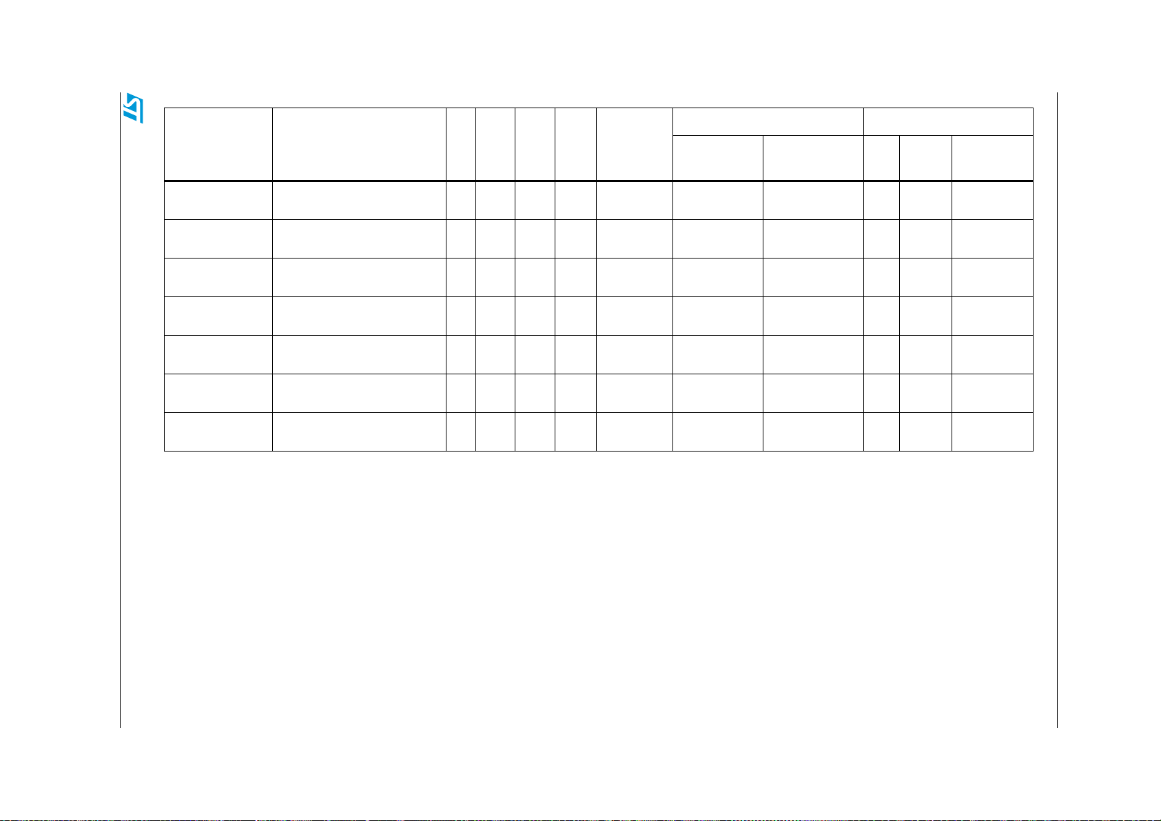
Table 4. SPC564A80 signal properties (continued)
PCR
P
Name Function
(1)
PA
A
Field
(2)
G
(3)
PCR
(4)
I/O
Type
Vol tag e
Pad Type
(5)
/
(6)
During Reset
Status
(7)
After
Reset
SPC564A74B4, SPC564A74L7, SPC564A80B4, SPC564A80L7 Pinout and signal description
Package pin #
176 208 324
Doc ID 15399 Rev 8 70/157
VDDEH4AB
VDDEH6
(27)
VDDEH6A
VDDEH6B
VDDEH6AB
VDDEH7
VDDEH7A
(27)
(27)
(26)
(27)
I/O Supply Input
I/O Supply Input
I/O Supply Input
I/O Supply Input
I/O Supply Input
I/O Supply Input
I/O Supply Input
(26)
— — I 3.3 V - 5.0 V I / — VDDEH4AB
— — I 3.3 V - 5.0 V I / — VDDEH6
— — I 3.3 V - 5.0 V I / — VDDEH6A
— — I 3.3 V - 5.0 V I / — VDDEH6B
— — I 3.3 V - 5.0 V I / — VDDEH6AB
—N9 W14
(27)
(27)
(27)
—— —
95 — —
110 — —
(27)
— F13 H19, U19
— — I 3.3 V - 5.0 V I / — VDDEH7 — D12 D15
— — I 3.3 V - 5.0 V I / — VDDEH7A 125 — —

71/157 Doc ID 15399 Rev 8
Table 4. SPC564A80 signal properties (continued)
Name Function
(1)
Pinout and signal description SPC564A74B4, SPC564A74L7, SPC564A80B4, SPC564A80L7
(7)
PCR
P
PA
Field
(3)
PCR
A
(2)
G
I/O
(4)
Type
Vol tag e
Pad Type
(5)
/
(6)
During Reset
Status
After
Reset
Package pin #
176 208 324
VDDEH7B
VSS Ground — — I — I / — VSS
I/O Supply Input
— — I 3.3 V - 5.0 V I / — VDDEH7B 138 — —
15,
29,
43,
57,
72,
90,
94,
96,
108,
115,
127,
133,
140
A1, A16,
B2, B15,
C3, C14,
D4, D13,
G7, G8,
G9,
G10,
H7, H8,
H9, H10,
J7, J8,
J9, J10,
K7,
K8, K9,
K10,
M16,
N4, N13,
P3, P14,
R2, R15,
T1, T16
A1, A22, B2,
B21, C3, C20,
D4, D19, J9,
J10, J11, J12,
J13, K9, K10,
K11, K12,
K13, K14, L9,
L10, L11, L12,
L13, L14,
M11, M12,
M13, M14, N9,
N10, N12,
N13, N14, P9,
P10, P12,
P13, P14,
T21, T22,
W4,W19, Y3,
Y20, AA2,
AA21, AB1,
AB22
1. For each pin in the table, each line in the Function column is a separate function of the pin. For all I/O pins the selection of primary pin function or secondary function or
GPIO is done in the SIU except where explicitly noted. See the Signal details table for a description of each signal.
2. The P/A/G column indicates the position a signal occupies in the muxing order for a pin—Primary, Alternate 1, Alternate 2, Alternate 3, or GPIO. Signals are selected by
setting the PA field value in the appropriate PCR register in the SIU module. The PA field values are as follows: P - 0b0001, A1 - 0b0010, A2 - 0b0100, A3 - 0b1000, or G 0b0000. Depending on the register, the PA field size can vary in length. For PA fields having fewer than four bits, remove the appropriate number of leading zeroes from
these values.
3. The Pad Configuration Register (PCR) PA field is used by software to select pin function.
4. Values in the PCR No. column refer to registers in the System Integration Unit (SIU). The actual register name is “SIU_PCR” suffixed by the PCR number. For example,
PCR[190] refers to the SIU register named SIU_PCR190.
5. The VDDE and VDDEH supply inputs are broken into segments. Each segment of slow I/O pins (VDDEH) may have a separate supply in the 3.3 V to 5.0 V range (10%/+5%). Each segment of fast I/O (VDDE) may have a separate supply in the 1.8 V to 3.3 V range (+/- 10%).
6. See Table 5 for details on pad types.

7. The Status During Reset pin is sampled after the internal POR is negated. Prior to exiting POR, the signal has a high impedance. Terminology is O - output, I - input, Up weak pull up enabled, Down - weak pull down enabled, Low - output driven low, High - output driven high. A dash for the function in this column denotes that both the input
and output buffer are turned off. The signal name to the left or right of the slash indicates the pin is enabled.
8. Output only.
9. When used as ETRIG, this pin must be configured as an input. For GPIO it can be configured either as an input or output.
10. Maximum frequency is 50 kHz.
11. The SIU_PCR219 register is unusual in that it controls pads for two separate device pins: GPIO[219] and MCKO. See the SPC564A80 Microcontroller Reference Manual
(SIU chapter) for details.
12. Multivoltage pads are automatically configured in low swing mode when a JTAG or Nexus function is selected, otherwise they are high swing.
13. On LQFP176 and LBGA208 packages, this pin is tied low internally.
14. Nexus multivoltage pads default to 5 V operation until the Nexus module is enabled.
15. EVTO
16. Do not connect pin directly to a power supply or ground.
17. This signal name is used to support legacy naming.
18. During and just after POR negates, internal pull resistors can be enabled, resulting in as much as 4 mA of current draw. The pull resistors are disabled when the system
Doc ID 15399 Rev 8 72/157
19. For pins AN12-AN15, if the analog features are used the VDDEH7 input pins should be tied to VDDA because that segment must meet the VDDA specification to support
20. Do not use VRC33 to drive external circuits.
21. VDDA0 and VDDA1 are shorted together internally in BGA packages. In the QFP package the two pads are double bonded on one pin called VDDA.
22. VSSA0 and VSSA1 are shorted together internally in BGA packages. In the QFP package the two pads are double bonded on one pin called VSSA.
23. VDDE2 and VDDE3 are shorted together in all production packages.
24. VDDE2 and VDDE3 are shorted together in all production packages.
25. VDDEH1A, VDDEH1B, and VDDEH1AB are shorted together in all production packages. The separation of the signal names is present to support legacy naming, however
26. VDDEH4, VDDEH4A, VDDEH4B, and VDDEH4AB are shorted together in all production packages. The separation of the signal names is present to support legacy
27. VDDEH6, VDDEH6A, VDDEH6B, and VDDEH6AB are shorted together in all production packages. The separation of the signal names is present to support legacy
should be clamped to 3.3 V to prevent possible damage to external tools that only support 3.3 V.
clock propagates through the device.
analog input function.
they should be considered as the same signal in this document.
naming, however they should be considered as the same signal in this document.
naming, however they should be considered as the same signal in this document.
SPC564A74B4, SPC564A74L7, SPC564A80B4, SPC564A80L7 Pinout and signal description

SPC564A74B4, SPC564A74L7, SPC564A80B4, SPC564A80L7 Pinout and signal description
Table 5. Pad types
Pad Type Name I/O Voltage Range
Slow pad_ssr_hv 3.0V - 5.5 V
Medium pad_msr_hv 3.0 V- 5.5 V
Fast pad_fc 3.0 V - 3.6 V
(1),(2)
MultiV
Analog pad_ae_hv 0.0 - 5.5 V
LVDS pad_lo_lv —
1. Multivoltage pads are automatically configured in low swing mode when a JTAG or Nexus function is
selected, otherwise they are high swing.
2. VDDEH7 supply cannot be below 4.5 V when in low-swing mode.
pad_multv_hv
3.0 V - 5.5 V (high swing mode)
3.0 V - 3.6 V (low swing mode)
2.5 Signal details
Table 6. Signal details
Signal Module or Function Description
CLKOUT Clock Generation
SPC564A80 clock output for the external/calibration bus
interface
ENGCLK Clock Generation Clock for external ASIC devices
EXTAL Clock Generation
Input pin for an external crystal oscillator or an external clock
source based on the value driven on the PLLREF pin at reset.
PLLREF is used to select whether the oscillator operates in xtal
mode or external reference mode from reset. PLLREF=0
selects external reference mode. On the 324BGA package,
PLLREF is bonded to the ball used for PLLCFG[0] for
compatibility with previous devices .
For the 176-pin QFP and 208-ball BGA packages:
0: External reference clock is selected.
1: XTAL oscillator mode is selected
PLLREF
Clock Generation
Reset/Configuration
For the 324 ball BGA package:
If RSTCFG is 0:
0: External reference clock is selected.
1: XTAL oscillator mode is selected.
If RSTCFG is 1, XTAL oscillator mode is selected.
XTAL Clock Generation Crystal oscillator input
DSPI_B_SCK_LVDSDSPI_B_SCK_LVDS+
DSPI_B_SOUT_LVDSDSPI_B_SOUT_LVDS+
DSPI LVDS pair used for DSPI_B TSB mode transmission
DSPI LVDS pair used for DSPI_B TSB mode transmission
Doc ID 15399 Rev 8 73/157

Pinout and signal description SPC564A74B4, SPC564A74L7, SPC564A80B4, SPC564A80L7
Table 6. Signal details (continued)
Signal Module or Function Description
DSPI_C_SCK_LVDSDSPI_C_SCK_LVDS+
DSPI_C_SOUT_LVDSDSPI_C_SOUT_LVDS+
PCS_B[0]
PCS_C[0]
PCS_D[0]
PCS_B[1:5]
PCS_C[1:5]
PCS_D[1:5]
SCK_B
SCK_C
SCK_D
SIN_B
SIN_C
SIN_D
SOUT_B
SOUT_C
SOUT_D
DSPI LVDS pair used for DSPI_C TSB mode transmission
DSPI LVDS pair used for DSPI_C TSB mode transmission
DSPI_B - DSPI_D
DSPI_B - DSPI_D
DSPI_B - DSPI_D
DSPI_B - DSPI_D DSPI data in
DSPI_B - DSPI_D DSPI data out
Peripheral chip select when device is in master mode—slave
select when used in slave mode
Peripheral chip select when device is in master mode—not
used in slave mode
DSPI clock—output when device is in master mode; input when
in slave mode
The ADDR[10:31] signals specify the physical address of the
bus transaction.
ADDR[10:31] EBI
ALE EBI
BDIP
[0:3] EBI
CS
DATA[0:31] EBI
OE
EBI
EBI
The 26 address lines correspond to bits 3-31 of the EBI’s 32-bit
internal address bus.
ADDR[15:31] can be used as Address and Data signals when
configured appropriately for a multiplexed external bus. This
allows 32-bit data operations, or 16-bit data operations without
using DATA[0:15] signals.
The Address Latch Enable (ALE) signal is used to demultiplex
the address from the data bus. It is asserted while the least
significant 16 bits of the address are present in the multiplexed
address/data bus.
is asserted to indicate that the master is requesting
BDIP
another data beat following the current one.
CSx is asserted by the master to indicate that this transaction is
targeted for a particular memory bank on the Primary external
bus.
The DATA[0:31] signals contain the data to be transferred for
the current transaction.
is used to indicate when an external memory is permitted to
OE
drive back read data. External memories must have their data
output buffers off when OE is negated. OE is only asserted for
chip-select accesses.
74/157 Doc ID 15399 Rev 8

SPC564A74B4, SPC564A74L7, SPC564A80B4, SPC564A80L7 Pinout and signal description
Table 6. Signal details (continued)
Signal Module or Function Description
RD_WR
TA
TS
WE
[2:3] EBI
[0:3]/BE[0:3] EBI
WE
eMIOS[0:23] eMIOS eMIOS I/O channels
AN[0:39] eQADC Single-ended analog inputs for analog-to-digital converter
FCK eQADC eQADC free running clock for eQADC SSI.
MA[0:2] eQADC
EBI
EBI
EBI
RD_WR
access or a write access.
TA
(and completed the access) for a write cycle, or returned data
for a read cycle. If the transaction is a burst read, TA
for each one of the transaction beats. For write transactions, TA
is only asserted once at access completion, even if more than
one write data beat is transferred.
The Transfer Start signal (TS
indicate the start of a transfer.
Write enables are used to enable program operations to a
particular memory. WE[2:3] are only asserted for write
accesses
Write enables are used to enable program operations to a
particular memory. These signals can also be used as byte
enables for read and write operation by setting the WEBS bit in
the appropriate EBI Base Register (EBI_BRn). WE
only asserted for write accesses. BE[0:3] are asserted for both
read and write accesses
These three control bits are output to enable the selection for
an external Analog Mux for expansion channels.
indicates whether the current transaction is a read
is asserted to indicate that the slave has received the data
is asserted
) is asserted by the SPC564A80 to
[0:3] are
REFBYPC eQADC Bypass capacitor input
SDI eQADC Serial data in
SDO eQADC Serial data out
SDS eQADC Serial data select
VRH eQADC Voltage reference high input
VRL eQADC Voltage reference low input
SCI_A_RX
SCI_B_RX
SCI_C_RX
SCI_A_TX
SCI_B_TX
SCI_C_TX
ETPU_A[0:31] eTPU eTPU I/O channel
eSCI_A - eSCI_C eSCI receive
eSCI_A - eSCI_C eSCI transmit
Doc ID 15399 Rev 8 75/157

Pinout and signal description SPC564A74B4, SPC564A74L7, SPC564A80B4, SPC564A80L7
Table 6. Signal details (continued)
Signal Module or Function Description
RCH0_[A:C]
RCH1_[A:C]
RCH2_[A:C]
RCH3_[A:C]
eTPU2
Reaction Module
RCH4_[A:C]
RCH5_[A:C]
TCRCLKA eTPU2 Input clock for TCR time base
CAN_A_TX
CAN_B_TX
CAN_C_TX
CAN_A_RX
CAN_B_RX
CAN_C_RX
FlexCan_A -
FlexCAN_C
FlexCAN_A -
FlexCAN_C
eTPU2 reaction channels. Used to control external actuators,
e.g., solenoid control for direct injection systems and valve
control in automatic transmissions
FlexCAN transmit
FlexCAN receive
FR_A_RX
FR_B_RX
FR_A_TX_EN
FR_B_TX_EN
FR_A_TX
FR_B_TX
FlexRay FlexRay receive (Channels A, B)
FlexRay FlexRay transmit enable (Channels A, B)
FlexRay Flexray transmit (Channels A, B)
JCOMP JTAG Enables the JTAG TAP controller.
TCK JTAG Clock input for the on-chip test logic.
TDI JTAG Serial test instruction and data input for the on-chip test logic.
TDO JTAG Serial test data output for the on-chip test logic.
TMS JTAG Controls test mode operations for the on-chip test logic.
is an input that is read on the negation of RESET to
EVTI
enable or disable the Nexus Debug port. After reset, the EVTI
EVTI
Nexus
pin is used to initiate program synchronization messages or
generate a breakpoint.
EVTO
Nexus
MCKO Nexus
Output that provides timing to a development tool for a single
watchpoint or breakpoint occurrence.
MCKO is a free running clock output to the development tools
which is used for timing of the MDO and MSEO
signals.
Trace message output to development tools. This pin also
MDO[0:11]
(1)
Nexus
indicates the status of the crystal oscillator clock following a
power-on reset, when MDO[0] is driven high until the crystal
oscillator clock achieves stability and is then negated.
MSEO
[0:1]
(1)
Nexus
Output pin—Indicates the start or end of the variable length
message on the MDO pins
Nexus Ready Output (RDY) is an output that indicates to the
RDY
Nexus
development tools the data is ready to be read from or written
to the Nexus read/write access registers.
76/157 Doc ID 15399 Rev 8

SPC564A74B4, SPC564A74L7, SPC564A80B4, SPC564A80L7 Pinout and signal description
Table 6. Signal details (continued)
Signal Module or Function Description
Two BOOTCFG signals are implemented in SPC564A80
MCUs.
The BAM program uses the BOOTCFG0 bit to determine
where to read the reset configuration word, and whether to
initiate a FlexCAN or eSCI boot.
The BOOTCFG1 pin is sampled during the assertion of the
RSTOUT signal, and the value is used to update the RSR and
the BAM boot mode
BOOTCFG[0:1] SIU - Configuration
WKPCFG SIU - Configuration
ETRIG[2:3] SIU - eQADC Triggers External signal eTRIGx triggers eQADC CFIFOx
GPIO[206] ETRIG0
(Input)
GPIO[207] ETRIG1
(Input)
SIU - eQADC Triggers External signal eTRIGx triggers eQADC CFIFOx
SIU - eQADC Triggers External signal eTRIGx triggers eQADC CFIFOx
See the SPC564A80 Microcontroller Reference Manual for
more information.
The following values are for BOOTCFG[0:1}:
00:Boot from internal flash memory
01:FlexCAN/eSCI boot
10:Boot from external memory using EBI
11:Reserved
Note: For the 176-pin QFP and 208-ball BGA packages
BOOTCFG[0] is always 0 since the EBI interface is not
available.
The WKPCFG pin is applied at the assertion of the internal
reset signal (assertion of RSTOUT
cycles before the negation of the RSTOUT
The value is used to configure whether the eTPU and eMIOS
pins are connected to internal weak pull up or weak pull down
devices after reset. The value latched on the WKPCFG pin at
reset is stored in the Reset Status Register (RSR), and is
updated for all reset sources except the Debug Port Reset and
Software External Reset.
0:Weak pulldown applied to eTPU and eMIOS pins at reset
1:Weak pullup applied to eTPU and eMIOS pins at reset.
), and is sampled 4 clock
pin.
Doc ID 15399 Rev 8 77/157

Pinout and signal description SPC564A74B4, SPC564A74L7, SPC564A80B4, SPC564A80L7
Table 6. Signal details (continued)
Signal Module or Function Description
IRQ[0:5]
IRQ[7:15]
NMI
GPIO[0:3]
GPIO[8:43]
GPIO[62:65]
GPIO[68:70]
GPIO[75:145]
GPIO[179:204]
GPIO[208:213]
GPIO[219]
GPIO[244:245]
RESET
SIU - External
Interrupts
SIU - External
Interrupts
SIU - GPIO
SIU - Reset
The IRQ
Register 1 is used to select the IRQ
[0:15] pins connect to the SIU IRQ inputs. IMUX Select
[0:15] pins as inputs to the
IRQs.
See the SPC564A80 Microcontroller Reference Manual for
more information.
Non-Maskable Interrupt
Configurable general purpose I/O pins. Each GPIO input and
output is separately controlled by an 8-bit input (GPDI) or
output (GPDO) register. Additionally, each GPIO pins is
configured using a dedicated SIU_PCR register.
The GPIO pins are generally multiplexed with other I/O pin
functions.
See The SPC564A80 Microcontroller Reference Manual for
more information.
–
The RESET
pin is an active low input. The RESET pin is
asserted by an external device during a power-on or external
reset. The internal reset signal asserts only if the RESET
pin
asserts for 10 clock cycles. Assertion of the RESET pin while
the device is in reset causes the reset cycle to start over.
The RESET
pin has a glitch detector which detects spikes
greater than two clock cycles in duration that fall below the
switch point of the input buffer logic of the VDDEH input pins.
The switch point lies between the maximum VIL and minimum
VIH specifications for the VDDEH input pins.
Used to enable or disable the PLLREF and the BOOTCFG[0:1]
configuration signals.
0:Get configuration information from BOOTCFG[0:1] and
RSTCFG SIU - Reset
PLLREF
1:Use default configuration of booting from internal flash with
crystal clock source
For the 176-pin QFP and 208-ball BGA packages RSTCFG is
always 0, so PLLREF and BOOTCFG signals are used.
The RSTOUT pin is an active low output that uses a push/pull
configuration. The RSTOUT pin is driven to the low state by the
RSTOUT SIU - Reset
MCU for all internal and external reset sources. There is a
delay between initiation of the reset and the assertion of the
RSTOUT pin.
1. Do not connect pin directly to a power supply or ground.
78/157 Doc ID 15399 Rev 8

SPC564A74B4, SPC564A74L7, SPC564A80B4, SPC564A80L7 Pinout and signal description
Table 7. Power/ground segmentation
Power Segment Voltage I/O Pins Powered by Segment
VDDE2 1.8 V - 3.3 V CS0, CS1, CS2, CS3,RD_WR, BDIP, WE0, WE1, OE, TS, TA
VDDE3 1.8 V - 3.3 V ADDR12, ADDR13, ADDR14, ADDR15
DATA0, DATA1, DATA2, DATA3, DATA4, DATA5, DATA6, DATA7,
VDDE5 1.8 V - 3.3 V
DATA8, DATA9, DATA10, DATA11, DATA12, DATA13, DATA14,
DATA15, CLKOUT, ENGCLK
CAL_CS0, CAL_CS2, CAL_CS3 CAL_ADDR12, CAL_ADDR13,
CAL_ADDR14, CAL_ADDR15, CAL_ADDR16, CAL_ADDR17,
CAL_ADDR18, CAL_ADDR19, CAL_ADDR20, CAL_ADDR21,
CAL_ADDR22, CAL_ADDR23, CAL_ADDR24, CAL_ADDR25,
VDDE12 1.8 V - 3.3 V
CAL_ADDR26, CAL_ADDR27, CAL_ADDR28, CAL_ADDR29,
CAL_ADDR30, CAL_DATA0, CAL_DATA1, CAL_DATA2,
CAL_DATA3, CAL_DATA4, CAL_DATA5, CAL_DATA6, CAL_DATA7,
CAL_DATA8, CAL_DATA9, CAL_DATA10, CAL_DATA11,
CAL_DATA12, CAL_DATA13, CAL_DATA14, CAL_DATA15,
CAL_RD_WR, CAL_WE0, CAL_WE1, CAL_OE, CAL_TS
ADDR16, ADDR17, ADDR18, ADDR19, ADDR20, ADDR21,
VDDE-EH 3.0 V - 5 V
ADDR22, ADDR23, ADDR24, ADDR25, ADDR26, ADDR27,
ADDR28, ADDR29, ADDR30, ADDR31
ETPUA10, ETPUA11, ETPUA12, ETPUA13, ETPUA14, ETPUA15,
VDDEH1 3.3 V - 5.0 V
ETPUA16, ETPUA17, ETPUA18, ETPUA19, ETPUA20, ETPUA21,
ETPUA22, ETPUA23, ETPUA24, ETPUA25, ETPUA26, ETPUA27,
ETPUA28, ETPUA29, ETPUA30, ETPUA31
EMIOS0, EMIOS1, EMIOS2, EMIOS3, EMIOS4, EMIOS5, EMIOS6,
EMIOS7, EMIOS8, EMIOS9, EMIOS10, EMIOS11, EMIOS12,
VDDEH4 3.3 V - 5.0 V
EMIOS13, EMIOS14, EMIOS15, EMIOS16, EMIOS17, EMIOS18,
EMIOS19, EMIOS20, EMIOS21, EMIOS22, EMIOS23, TCRCLKA,
ETPUA0, ETPUA1, ETPUA2, ETPUA3, ETPUA4, ETPUA5,
ETPUA6, ETPUA7, ETPUA8, ETPUA9, ETPUA0
, RSTOUT, PLLREF, PLLCFG1, RSTCFG, BOOTCFG0,
RESET
BOOTCFG1, WKPCFG, CAN_A_TX, CAN_A_RX, CAN_B_TX,
CAN_B_RX, CAN_C_TX, CAN_C_RX, SCI_A_TX, SCI_A_RX,
VDDEH6 3.3 V - 5.0 V
SCI_B_TX, SCI_C_RX, DSPI_B_SCK, DSPI_B_SIN,
DSPI_B_SOUT, DSPI_B_PCS[0], DSPI_B_PCS[1],
DSPI_B_PCS[2], DSPI_B_PCS[3], DSPI_B_PCS[4],
DSPI_B_PCS[5], SCI_B_RX, SCI_C_TX, EXTAL, XTAL
VDDEH7 3.3 V - 5.0 V
VDDA 5 V
VRC33
(1)
3.3 V MCKO, MDO0, MDO1, MDO2, MDO3
EMIOS14, EMIOS 15, GPIO98, GPIO99, GPIO203, GPIO204,
GPIO206, GPIO207, GPIO219, EVTI, EVTO, MDO4, MDO5,
MDO6, MDO7, MDO8, MDO9, MDO10, MDO11, MSEO0, MSEO1,
RDY, TCK, TDI, TDO, TMS, JCOMP, DSPI_A_SCK, DSPI_A_SIN,
DSPI_A_SOUT, DSPI_A_PCS[0], DSPI_A_PCS[1],
DSPI_A_PCS[4], DSPI_A_PCS[5], AN12-SDS, AN13-SDO, AN14SDI, AN15-FCK
AN0, AN1, AN2, AN3, AN4, AN5, AN6, AN7, AN8, AN9, AN10,
AN11, AN16, AN17, AN18, AN19, AN20, AN21, AN22, AN23,
AN24, AN25, AN26, AN27, AN28, AN29, AN30, AN31, AN32,
AN33, AN34, AN35, AN36, AN37, AN38, AN39, VRH, VRL,
REFBYBC
Doc ID 15399 Rev 8 79/157

Pinout and signal description SPC564A74B4, SPC564A74L7, SPC564A80B4, SPC564A80L7
Table 7. Power/ground segmentation (continued)
Power Segment Voltage I/O Pins Powered by Segment
Other Power Segments
VDDREG 5 V —
VRCCTL — —
VDDPLL 1.2 V —
0.95–1.2 V
(unregulated mode)
VSTBY
2.0–5.5 V (regulated
mode)
VSS — —
1. Do not use VRC33 to drive external circuits.
—
—
80/157 Doc ID 15399 Rev 8

SPC564A74B4, SPC564A74L7, SPC564A80B4, SPC564A80L7 Electrical characteristics
3 Electrical characteristics
This section contains detailed information on power considerations, DC/AC electrical
characteristics, and AC timing specifications for the SPC564A80 series of MCUs.
The electrical specifications are preliminary and are from previous designs, design
simulations, or initial evaluation. These specifications may not be fully tested or guaranteed
at this early stage of the product life cycle, however for production silicon these
specifications will be met. Finalized specifications will be published after complete
characterization and device qualifications have been completed.
In the tables where the device logic provides signals with their respective timing
characteristics, the symbol “CC” for Controller Characteristics is included in the Symbol
column.
In the tables where the external system must provide signals with their respective timing
characteristics to the device, the symbol “SR” for System Requirement is included in the
Symbol column.
3.1 Parameter classification
The electrical parameters shown in this supplement are guaranteed by various methods. To
give the customer a better understanding, the classifications listed in Ta bl e 8 are used and
the parameters are tagged accordingly in the tables where appropriate.
Table 8. Parameter classifications
Classification tag Tag description
P Those parameters are guaranteed during production testing on each individual device.
C
T
D Those parameters are derived mainly from simulations.
Those parameters are achieved by the design characterization by measuring a statistically
relevant sample size across process variations.
Those parameters are achieved by design characterization on a small sample size from typical
devices under typical conditions unless otherwise noted. All values shown in the typical
column are within this category.
Note: The classification is shown in the column labeled “C” in the parameter tables where
appropriate.
Doc ID 15399 Rev 8 81/157

Electrical characteristics SPC564A74B4, SPC564A74L7, SPC564A80B4, SPC564A80L7
3.2 Maximum ratings
Table 9. Absolute maximum ratings
Symbol Parameter Conditions
V
V
FLASH
V
STBY
V
DDPLL
V
RC33
V
V
V
DDEH
V
DD
DDA
DDE
IN
SR 1.2 V core supply voltage
SR Flash core voltage
(3),(4)
SR SRAM standby voltage
SR Clock synthesizer voltage –0.3 1.32 V
Voltage regulator control input
SR
voltage
(4)
SR Analog supply voltage
SR I/O supply voltage
SR I/O supply voltage
SR DC input voltage
(4),(6)
(5)
(7)
(1)
(5)
(5)
(2)
Reference to V
V
powered I/O pads –1.0
DDEH
powered I/O pads –1.0
V
DDE
SSA
Val ue
Unit
min max
–0.3 1.32 V
–0.3 3.6 V
–0.3 6 V
–0.3 3.6 V
–0.3 5.5 V
–0.3 3.6 V
–0.3 5.5 V
V
DDEH
0.3 V
V
DDE
0.3 V
(9)
(10)
+
+
(8)
(10)
V
V
V
V
V
SSPLL
V
DDREG
V
– V
SS
RH
– V
RL
I
MAXD
I
MAXA
RH
– V
– V
SSA
RL
SSA
V
powered I/O pads –1.0 5.5
DDA
Voltage regulator supply
SR
voltage
–0.3 5.5 V
SR Analog reference high voltage Reference to VRL –0.3 5.5 V
SR VSS differential voltage –0.1 0.1 V
SS
SR V
SR
SR
SR
SR
differential voltage –0.3 5.5 V
REF
VRL to V
voltage
V
SSPLL
voltage
Maximum DC digital input
current
Maximum DC analog input
current
differential
SSA
to VSS differential
(11)
(12)
Per pin, applies to all digital
pins
Per pin, applies to all
analog pins
–0.3 0.3 V
–0.1 0.1 V
–3 3 mA
—5mA
82/157 Doc ID 15399 Rev 8

SPC564A74B4, SPC564A74L7, SPC564A80B4, SPC564A80L7 Electrical characteristics
Table 9. Absolute maximum ratings
(1)
(continued)
Val ue
Symbol Parameter Conditions
Unit
min max
Maximum operating
T
J
SR
temperature range - die
–40.0 150.0
junction temperature
T
STG
T
SDR
MSL SR Moisture sensitivity level
1. Functional operating conditions are given in the DC electrical specifications. Absolute maximum ratings are stress ratings
only, and functional operation at the maxima is not guaranteed. Stress beyond the listed maxima may affect device
reliability or cause permanent damage to the device.
2. Allowed 2 V for 10 hours cumulative time, remaining time at 1.2 V +10%.
3. The V
4. Allowed 5.3 V for 10 hours cumulative time, remaining time at 3.3 V +10%.
5. Allowed 5.9 V for 10 hours cumulative time, remaining time at 5 V +10%.
6. All functional non-supply I/O pins are clamped to V
7. AC signal overshoot and undershoot of up to 2.0 V of the input voltages is permitted for an accumulative duration of 60
8. Internal structures hold the voltage greater than –1.0 V if the injection current limit of 2 mA is met.
9. Internal structures hold the input voltage less than the maximum voltage on all pads powered by V
10. Internal structures hold the input voltage less than the maximum voltage on all pads powered by V
11. Total injection current for all pins (including both digital and analog) must not exceed 25 mA.
12. Total injection current for all analog input pins must not exceed 15 mA.
13. Solder profile per IPC/JEDEC J-STD-020D.
14. Moisture sensitivity per JEDEC test method A112.
FLASH
devices only.
hours over the complete lifetime of the device (injection current not limited for this duration).
maximum injection current specification is met (2 mA for all pins) and V
maximum injection current specification is met (2 mA for all pins) and V
SR Storage temperature range –55.0 150.0
Maximum solder
SR
temperature
supply is connected to V
(13)
(14)
in the package substrate. This specification applies to calibration package
RC33
SS
and V
DDE
, or V
.
DDEH
is within the operating voltage specifications.
DDEH
is within the operating voltage specifications.
DDE
— 260.0
—3
DDEH
DDE
supplies, if the
supplies, if the
o
C
o
C
o
C
3.3 Thermal characteristics
Table 10. Thermal characteristics for 176-pin QFP
Symbol C Parameter Conditions Value Unit
R
R
R
R
R
θJA
θJA
θJMA
θJMA
θJB
CC D Junction-to-Ambient, Natural Convection
CC D Junction-to-Ambient, Natural Convection
CC D Junction-to-Moving-Air, Ambient
CC D Junction-to-Moving-Air, Ambient
CC D Junction-to-Board
(3)
Doc ID 15399 Rev 8 83/157
(2)
(2)
(1)
(2)
Single layer board - 1s 38 °C/W
(2)
Four layer board - 2s2p 31 °C/W
200 ft./min., single layer
board - 1s
at 200 ft./min., four layer
board - 2s2p
30 °C/W
25 °C/W
20 °C/W

Electrical characteristics SPC564A74B4, SPC564A74L7, SPC564A80B4, SPC564A80L7
Table 10. Thermal characteristics for 176-pin QFP
(1)
(continued)
Symbol C Parameter Conditions Value Unit
(5)
(4)
5°C/W
2°C/W
(1)
R
θJCtop
Ψ
JT
1. Thermal characteristics are targets based on simulation that are subject to change per device characterization.
2. Junction-to-Ambient Thermal Resistance determined per JEDEC JESD51-3 and JESD51-6. Thermal test board meets
JEDEC specification for this package.
3. Junction-to-Board thermal resistance determined per JEDEC JESD51-8. Thermal test board meets JEDEC specification
for the specified package.
4. Junction-to-Case at the top of the package determined using MIL-STD 883 Method 1012.1. The cold plate temperature is
used for the case temperature. Reported value includes the thermal resistance of the interface layer.
5. Thermal characterization parameter indicating the temperature difference between the package top and the junction
temperature per JEDEC JESD51-2. When Greek letters are not available, the thermal characterization parameter is written
as Psi-JT.
Table 11. Thermal characteristics for 208-pin LBGA
CC D Junction-to-Case
CC D
Junction-to-Package Top, Natural
Convection
Symbol C Parameter Conditions Value Unit
R
θJA
R
θJA
CC D
CC D
Junction-to-Ambient, Natural
Convection
Junction-to-Ambient, Natural
Convection
(2),(3)
(2),(4)
One layer board - 1s 39 °C/W
Four layer board - 2s2p 24 °C/W
R
θJMA
R
θJMA
R
θJB
R
θJC
Ψ
JT
1. Thermal characteristics are targets based on simulation that are subject to change per device characterization.
2. Junction temperature is a function of die size, on-chip power dissipation, package thermal resistance, mounting site (board)
temperature, ambient temperature, air flow, power dissipation of other components on the board, and board thermal
resistance.
3. Per SEMI G38-87 and JEDEC JESD51-2 with the single-layer board horizontal.
4. Per JEDEC JESD51-6 with the board horizontal.
5. Thermal resistance between the die and the printed circuit board per JEDEC JESD51-8. Board temperature is measured
on the top surface of the board near the package.
6. Indicates the average thermal resistance between the die and the case top surface as measured by the cold plate method
(MIL SPEC-883 Method 1012.1) with the cold plate temperature used for the case temperature.
7. Thermal characterization parameter indicating the temperature difference between package top and the junction
temperature per JEDEC JESD51-2. When Greek letters are not available, the thermal characterization parameter is written
as Psi-JT.
CC D Junction-to-Moving-Air, Ambient
CC D Junction-to-Moving-Air, Ambient
CC D Junction-to-board
CC D Junction-to-case
CC D
Junction-to-package top natural
convection
(5)
(6)
(7)
(2),(4)
(2),(4)
at 200 ft./min., one layer
board
at 200 ft./min., four layer
board 2s2p
31 °C/W
20 °C/W
Four layer board - 2s2p 13 °C/W
6°C/W
2°C/W
84/157 Doc ID 15399 Rev 8

SPC564A74B4, SPC564A74L7, SPC564A80B4, SPC564A80L7 Electrical characteristics
Table 12. Thermal characteristics for 324-pin PBGA
(1)
Symbol C Parameter Conditions Value Unit
R
θJA
R
θJA
R
θJMA
R
θJMA
R
θJB
R
θJCtop
Ψ
JT
1. Thermal characteristics are targets based on simulation that are subject to change per device characterization.
2. Junction-to-Ambient Thermal Resistance determined per JEDEC JESD51-3 and JESD51-6. Thermal test board meets
JEDEC specification for this package.
3. Junction-to-Board thermal resistance determined per JEDEC JESD51-8. Thermal test board meets JEDEC specification
for the specified package.
4. Junction-to-Case at the top of the package determined using MIL-STD 883 Method 1012.1. The cold plate temperature is
used for the case temperature. Reported value includes the thermal resistance of the interface layer.
5. Thermal characterization parameter indicating the temperature difference between the package top and the junction
temperature per JEDEC JESD51-2. When Greek letters are not available, the thermal characterization parameter is written
as Psi-JT.
CC D Junction-to-Ambient, Natural Convection
CC D Junction-to-Ambient, Natural Convection
CC D Junction-to-Moving-Air, Ambient
CC D Junction-to-Moving-Air, Ambient
CC D Junction-to-Board
CC D Junction-to-Case
CC D
Junction-to-Package Top, Natural
Convection
(3)
(4)
(5)
(2)
(2)
(2)
Single layer board - 1s 31 °C/W
(2)
Four layer board - 2s2p 23 °C/W
at 200 ft./min., single
layer board
at 200 ft./min., four layer
board 2s2p
23 °C/W
17 °C/W
11 °C/W
7°C/W
2°C/W
3.3.1 General notes for specifications at maximum junction temperature
An estimation of the chip junction temperature, TJ, can be obtained from the equation:
Equation 1 T
where:
T
A
R
θJA
P
= power dissipation in the package (W)
D
The thermal resistance values used are based on the JEDEC JESD51 series of standards
to provide consistent values for estimations and comparisons. The difference between the
values determined for the single-layer (1s) board compared to a four-layer board that has
two signal layers, a power and a ground plane (2s2p), demonstrate that the effective thermal
resistance is not a constant. The thermal resistance depends on the:
● Construction of the application board (number of planes)
● Effective size of the board which cools the component
● Quality of the thermal and electrical connections to the planes
● Power dissipated by adjacent components
Connect all the ground and power balls to the respective planes with one via per ball. Using
fewer vias to connect the package to the planes reduces the thermal performance. Thinner
planes also reduce the thermal performance. When the clearance between the vias leave
the planes virtually disconnected, the thermal performance is also greatly reduced.
= TA + (R
J
θJA
* PD)
= ambient temperature for the package (oC)
= junction-to-ambient thermal resistance (oC/W)
Doc ID 15399 Rev 8 85/157

Electrical characteristics SPC564A74B4, SPC564A74L7, SPC564A80B4, SPC564A80L7
As a general rule, the value obtained on a single-layer board is within the normal range for
the tightly packed printed circuit board. The value obtained on a board with the internal
planes is usually within the normal range if the application board has:
● One oz. (35 micron nominal thickness) internal planes
● Components are well separated
● Overall power dissipation on the board is less than 0.02 W/cm
2
The thermal performance of any component depends on the power dissipation of the
surrounding components. In addition, the ambient temperature varies widely within the
application. For many natural convection and especially closed box applications, the board
temperature at the perimeter (edge) of the package is approximately the same as the local
air temperature near the device. Specifying the local ambient conditions explicitly as the
board temperature provides a more precise description of the local ambient conditions that
determine the temperature of the device.
At a known board temperature, the junction temperature is estimated using the following
equation:
Equation 2 T
= TB + (R
J
θJB
* PD)
where:
T
= board temperature for the package perimeter (oC)
B
R
= junction-to-board thermal resistance (oC/W) per JESD51-8S
θJB
P
= power dissipation in the package (W)
D
When the heat loss from the package case to the air does not factor into the calculation, an
acceptable value for the junction temperature is predictable. Ensure the application board is
similar to the thermal test condition, with the component soldered to a board with internal
planes.
The thermal resistance is expressed as the sum of a junction-to-case thermal resistance
plus a case-to-ambient thermal resistance:
Equation 3 R
θJA
= R
θJC
+ R
θCA
where:
R
= junction-to-ambient thermal resistance (oC/W)
θJA
R
= junction-to-case thermal resistance (oC/W)
θJC
R
= case to ambient thermal resistance (oC/W)
θCA
R
is device related and is not affected by other factors. The thermal environment can be
θJC
controlled to change the case-to-ambient thermal resistance, R
. For example, change
θCA
the air flow around the device, add a heat sink, change the mounting arrangement on the
printed circuit board, or change the thermal dissipation on the printed circuit board
surrounding the device. This description is most useful for packages with heat sinks where
90% of the heat flow is through the case to heat sink to ambient. For most packages, a
better model is required.
A more accurate two-resistor thermal model can be constructed from the junction-to-board
thermal resistance and the junction-to-case thermal resistance. The junction-to-case
thermal resistance describes when using a heat sink or where a substantial amount of heat
is dissipated from the top of the package. The junction-to-board thermal resistance
describes the thermal performance when most of the heat is conducted to the printed circuit
86/157 Doc ID 15399 Rev 8

SPC564A74B4, SPC564A74L7, SPC564A80B4, SPC564A80L7 Electrical characteristics
board. This model can be used to generate simple estimations and for computational fluid
dynamics (CFD) thermal models.
To determine the junction temperature of the device in the application on a prototype board,
use the thermal characterization parameter (Ψ
) to determine the junction temperature by
JT
measuring the temperature at the top center of the package case using the following
equation:
Equation 4 T
= TT + (ΨJT x PD)
J
where:
T
= thermocouple temperature on top of the package (oC)
T
Ψ
= thermal characterization parameter (oC/W)
JT
P
= power dissipation in the package (W)
D
The thermal characterization parameter is measured in compliance with the JESD51-2
specification using a 40-gauge type T thermocouple epoxied to the top center of the
package case. Position the thermocouple so that the thermocouple junction rests on the
package. Place a small amount of epoxy on the thermocouple junction and approximately 1
mm of wire extending from the junction. Place the thermocouple wire flat against the
package case to avoid measurement errors caused by the cooling effects of the
thermocouple wire.
References:
Semiconductor Equipment and Materials International
3081 Zanker Road
San Jose, CA 95134
USA
(408) 943-6900
MIL-SPEC and EIA/JESD (JEDEC) specifications are available from Global Engineering
Documents at 800-854-7179 or 303-397-7956.
JEDEC specifications are available on the WEB at http://www.jedec.org.
● C.E. Triplett and B. Joiner, “An Experimental Characterization of a 272 PBGA Within an
Automotive Engine Controller Module,” Proceedings of SemiTherm, San Diego, 1998,
pp. 47-54.
● G. Kromann, S. Shidore, and S. Addison, “Thermal Modeling of a PBGA for Air-Cooled
Applications”, Electronic Packaging and Production, pp. 53-58, March 1998.
● B. Joiner and V. Adams, “Measurement and Simulation of Junction to Board Thermal
Resistance and Its Application in Thermal Modeling,” Proceedings of SemiTherm, San
Diego, 1999, pp. 212-220.
Doc ID 15399 Rev 8 87/157

Electrical characteristics SPC564A74B4, SPC564A74L7, SPC564A80B4, SPC564A80L7
3.4 EMI (electromagnetic interference) characteristics
Table 13. EMI Testing Specifications
Symbol Parameter Conditions Clocks
(1)
Frequency
150 kHz – 50
50 – 150 MHz 20
150 – 500 MHz 26
500 – 1000 MHz 26
V
DDREG
=5.25V;
TA=25°C
16 MHz crystal
40 MHz bus
No PLL frequency
modulation
IEC Level K —
Radiated
emissions,
electric field
V
RE_TEM
150 kHz – 30 MHz
RBW 9 kHz, Step
Size 5 kHz
30 MHz – 1 GHz RBW 120 kHz,
Step Size 80 kHz
16 MHz crystal
40 MHz bus
± 2% PLL
frequency
modulation
SAE Level 3 —
150 kHz– 50
50 – 150 MHz 13
150 – 500 MHz 11
500 – 1000 MHz 13
IEC Level L —
SAE Level 2 —
1. EMI testing and I/O port waveforms per SAE J1752/3 issued 1995-03 and IEC 61967-2.
Range
MHz
MHz
Level
(Max)
20
13
Unit
dBμV
dBμV
3.5 Electrostatic discharge (ESD) characteristics
Table 14. ESD ratings
Symbol Parameter Conditions Value Unit
— SR ESD for Human Body Model (HBM) — 2000 V
R1 SR
C SR — 100 pF
—SR
— SR Number of pulses per pin
— SR Number of pulses — 1 —
1. All ESD testing is in conformity with CDF-AEC-Q100 Stress Test Qualification for Automotive Grade Integrated Circuits.
2. Device failure is defined as: “If after exposure to ESD pulses, the device does not meet the device specification
requirements, which includes the complete DC parametric and functional testing at room temperature and hot
temperature.”
(1),(2)
HBM circuit description
ESD for field induced charge Model
(FDCM)
— 1500 Ω
All pins 500
Corner pins 750
Positive pulses (HBM) 1 —
Negative pulses (HBM) 1 —
V
88/157 Doc ID 15399 Rev 8

SPC564A74B4, SPC564A74L7, SPC564A80B4, SPC564A80L7 Electrical characteristics
3.6 Power management control (PMC) and power on reset (POR)
electrical specifications
Table 15. PMC Operating Conditions and External Regulators Supply Voltage
ID Name Parameter Min Typ Max Unit
1 Jtemp SR — Junction temperature –40 27 150 °C
2 Vddreg SR — PMC 5 V supply voltage V
Core supply voltage 1.2 V V
3VddSR—
regulator is used without disabling the internal
regulator (PMC unit turned on, LVI monitor
(1)
active)
Core supply voltage 1.2 V V
3a — SR —
regulator is used with a disabled internal
regulator (PMC unit turned-off, LVI monitor
DDREG
when external
DD
when external
DD
4.75 5 5.25 V
(2)
1.26
1.3 1.32 V
1.14 1.2 1.32 V
disabled)
4IvddSR—
Voltage regulator core supply maximum
required DC output current
445 — — mA
Regulated 3.3 V supply voltage when external
regulator is used without disabling the internal
5 Vdd33 SR —
regulator (PMC unit turned-on, internal 3.3V
3.3 3.45 3.6 V
regulator enabled, LVI
monitor active)
(3)
Regulated 3.3 V supply voltage when external
5a — SR —
regulator is used
regulator
with a disabled internal
(PMC unit turned-off, LVI monitor
33.33.6V
disabled)
6—SR—
1. An internal regulator controller can be used to regulate core supply.
2. The minimum supply required for the part to exit reset and enter in normal run mode is 1.28 V.
3. An internal regulator can be used to regulate 3.3 V supply.
Voltage regulator 3.3 V supply maximum
required DC output current
80 — — mA
Table 16. PMC Electrical Characteristics
ID Name Parameter Min Typ Max Unit Notes
1 VBG CC C
1a — CC P
1b — CC P
1c — CC C
1d — CC C
Nominal bandgap voltage
reference
Untrimmed bandgap
reference voltage
Trimmed bandgap reference
voltage (5 V, 27 °C)
Bandgap reference
temperature variation
Bandgap reference supply
voltage variation
—1.219— V
VBG - 7% VBG Vbg + 6% V
VBG -10mV VBG
VBG +
10mV
V
—100—ppm/°C
— 3000 — ppm/V
Doc ID 15399 Rev 8 89/157
Electrical characteristics SPC564A74B4, SPC564A74L7, SPC564A80B4, SPC564A80L7
Table 16. PMC Electrical Characteristics (continued)
ID Name Parameter Min Typ Max Unit Notes
Nominal V
2VddCCC
internal regulator target DC
output voltage
Nominal V
2a — CC P
internal regulator target DC
output voltage variation at
core supply
DD
(1)
core supply
DD
—1.28—V
Vdd - 6% Vdd Vdd + 10% V
power-on reset
core supply
DD
Vdd -
10%
(2)
Vdd Vdd + 3% V
2b — CC P
Nominal V
internal regulator target DC
output voltage variation
after power-on reset
2c — CC C Trimming step Vdd — 20 — mV
Voltage regulator controller
2d Ivrcctl CC C
for core supply maximum
20 — — mA
DC output current
3 Lvi1p2 CC C
Nominal LVI for rising core
(3)
supply
—1.160— V
Variation of LVI for rising
3a — CC C
core supply at power-on
1.120 1.200 1.280 V See note
reset
3b — CC C
3c — CC C
Variation of LVI for rising
core supply after power-on
reset
Trimming step LVI core
supply
Lvi1p2 - 3% Lvi1p2
—20—mV
Lvi1p2 +
3%
VSee note
3d Lvi1p2_h CC C LVI core supply hysteresis — 40 — mV
4 Por1.2V_r CC C POR 1.2 V rising — 0.709 — V
(4)
(4)
4a — CC C POR 1.2 V rising variation
Por1.2V_r -
35%
Por1.2V_r
Por1.2 V_r +
35%
4b Por1.2V_f CC C POR 1.2 V falling — 0.638 — V
4c — CC C POR 1.2 V falling variation
Por1.2V_f -
35%
Por1.2V_f
Por1.2V_f +
35%
Nominal 3.3 V supply
5 Vdd33 CC C
internal regulator DC output
—3.39—V
voltage
Nominal 3.3 V supply
5a — CC P
internal regulator DC output
voltage variation at power-
Vdd33 -
8.5%
Vdd33 Vdd3 + 7% V See note
on reset
Nominal 3.3 V supply
5b — CC P
internal regulator DC output
voltage variation power-on
Vdd33 -
7.5%
Vdd33
Vdd33 +
7%
reset
90/157 Doc ID 15399 Rev 8
V
V
With internal
load up
V
to Idd3p3
(5)

SPC564A74B4, SPC564A74L7, SPC564A80B4, SPC564A80L7 Electrical characteristics
Table 16. PMC Electrical Characteristics (continued)
ID Name Parameter Min Typ Max Unit Notes
Voltage regulator 3.3 V
5c — CC D
5d Idd3p3 CC P
output impedance at
maximum DC load
Voltage regulator 3.3 V
maximum DC output current
(internal regulator
enabled)
(6)
—— 2Ω
(7)
80
——mA
5e Vdd33 ILim CC C
6 Lvi3p3 CC C
6a — CC C
6b — CC C
Voltage regulator 3.3 V DC
current limit
Nominal LVI for rising 3.3 V
supply
Variation of LVI for rising
3.3 V supply at power-on
reset
Variation of LVI for rising
3.3 V supply after power-on
reset
—130—mA
—3.090— V
Lvi3p3 - 6% Lvi3p3
Lvi3p3 - 3% Lvi3p3
Lvi3p3 +
6%
Lvi3p3 +
3%
VSee note
VSee note
6c — CC C Trimming step LVI 3.3 V — 20 — mV
6d Lvi3p3_h CC C LVI 3.3 V hysteresis — 60 — mV
7 Por3.3V_r CC C
7a — CC C
7b Por3.3V_f CC C
7c — CC C
Nominal POR for rising
3.3 V supply
Variation of POR for rising
3.3 V supply
Nominal POR for falling
3.3 V supply
Variation of POR for falling
3.3 V supply
—2.07—V
Por3.3V_r-
35%
Por3.3V_r
Por3.3 V_r +
35%
—1.95—V
Por3.3V_f -
35%
Por3.3V_f
Por3.3V_f +
35%
V
V
The Lvi3p3
specs are
also valid for
the Vddeh
LV I
(8)
(8)
The 3.3V
POR specs
are also valid
for the V
DDEH
POR
8 Lvi5p0 CC C
8a — CC C
8b — CC C
Nominal LVI for rising 5 V
DDREG
supply
V
Variation of LVI for rising 5 V
V
supply at power-on
DDREG
reset
Variation of LVI for rising 5 V
V
G supply power-on
DDRE
reset
—4.290— V
Lvi5p0 - 6% Lvi5p0
Lvi5p0 - 3% Lvi5p0
Lvi5p0 +
6%
Lvi5p0 +
3%
V
V
8c — CC C Trimming step LVI 5 V — 20 — mV
8d Lvi5p0_h CC C LVI 5 V hysteresis — 60 — mV
Doc ID 15399 Rev 8 91/157

Electrical characteristics SPC564A74B4, SPC564A74L7, SPC564A80B4, SPC564A80L7
Table 16. PMC Electrical Characteristics (continued)
ID Name Parameter Min Typ Max Unit Notes
9 Por5V_r CC C
9a — CC C
9b Por5V_f CC C
9c — CC C
1. Using external ballast transistor.
2. Min range is extended to 10% since Lvi1p2 is reprogrammed from 1.2 V to 1.16 V after power-on reset.
3. LVI for falling supply is calculated as LVI rising – LVI hysteresis.
4. Lvi1p2 tracks DC target variation of internal Vdd regulator. Minimum and maximum Lvi1p2 correspond to minimum and
maximum Vdd DC target respectively.
5. Minimum loading (<10 mA) for reading trim values from flash, powering internal RC oscillator, and IO consumption during
POR.
6. No external load is allowed, except for use as a reference for an external tool.
7. This value is valid only when the internal regulator is bypassed. When the internal regulator is enabled, the maximum
external load allowed on the Nexus pads is 30 pF at 40 MHz.
8. Lvi3p3 tracks DC target variation of internal Vdd33 regulator. Minimum and maximum Lvi3p3 correspond to minimum and
maximum Vdd33 DC target respectively.
Nominal POR for rising 5 V
DDREG
supply
V
Variation of POR for rising
DDREG
supply
5V V
Nominal POR for falling 5 V
V
DDREG
supply
Variation of POR for falling
DDREG
supply
5V V
—2.67—V
Por5V_r
- 35%
Por5V_r
Por5V_r
+ 50%
V
—2.47—V
Por5V_f
- 35%
Por5V_f
Por5V_f
+ 50%
V
3.6.1 Regulator Example
In designs where the SPC564A80 microcontroller’s internal regulators are used, a ballast is
required for generation of the 1.2 V internal supply. No ballast is required when an external
1.2 V supply is used.
92/157 Doc ID 15399 Rev 8

SPC564A74B4, SPC564A74L7, SPC564A80B4, SPC564A80L7 Electrical characteristics
The resistor may or may not be
required. This depends on the
allowable power dissipation of
the npn bypass transistor
device. The resistor may be
used to limit the in-rush current
at power on.
Rc
Creg
V
DDREG
The bypass transistor
MUST be operated out
of saturation region.
Mandatory decoupling
Cc
Re
Keep parasitic inductance
under 20nH
V
RCCTL
Rb
Cb
MCU
V
DD
capacitor network
V
SS
Ce Cd
VRCCTL capacitor and resistor is required
Figure 8. Core voltage regulator controller external components preferred
configuration
Table 17. SPC564A80 External network specification
External Network
Parameter
T1
Cb 1.1 μF2.2μF2.97μF X7R,-50%/+35%
Min Typ Max Comment
NJD2873 or BCP68
only
Ce 3*2.35μF+5μF3*4.7μF+10μF3*6.35μF+13.5μF X7R, -50%/+35%
Equivalent ESR of Ce
capacitors
5m 50m
ΩΩ
Cd 4*50nF 4*100nF 4*135nF X7R, -50%/+35%
Rb 9 10 11 +/-10%
Re 0.252 0.280 0.308 +/-10%
Creg 10μF
ΩΩΩ
ΩΩΩ
It depends on
external Vreg.
Cc 5μF10μF13.5μF X7R, -50%/+35%
May or may not be
required. It depends
Rc 1.1 5.6
ΩΩ
on the allowable
power dissipation of
T1.
Doc ID 15399 Rev 8 93/157

Electrical characteristics SPC564A74B4, SPC564A74L7, SPC564A80B4, SPC564A80L7
3.6.2 Recommended power transistors
The following NPN transistors are recommended for use with the on-chip voltage regulator
controller: ON Semiconductor
TM
BCP68T1 or NJD2873 as well as Philips SemiconductorTM
BCP68. The collector of the external transistor is preferably connected to the same voltage
supply source as the output stage of the regulator.
Table 18. Recommended operating characteristics
Symbol Parameter Value Unit
(β) DC current gain (Beta) 60 – 550 —
h
FE
P
I
CMaxDC
VCE
V
1. Adjust resistor at bipolar transistor collector for 3.3 V/5.0 V to avoid VCE < VCE
Absolute minimum power dissipation
D
Minimum peak collector current 1.0 A
Collector-to-emitter saturation voltage 200 – 600
SAT
Base-to-emitter voltage 0.4 – 1.0 V
BE
3.7 Power up/down sequencing
There is no power sequencing required among power sources during power up and power
down, in order to operate within specification.
Although there are no power up/down sequencing requirements to prevent issues such as
latch-up or excessive current spikes the state of the I/O pins during power up/down varies
according to Ta bl e 1 9 for all pins with fast pads, and Tab le 2 0 for all pins with medium, slow,
and multi-voltage pads.
Table 19. Power sequence pin states (fast pads)
>1.0
(1.5 preferred)
(1)
.
SAT
W
mV
V
DDE
V
RC33
V
DD
LOW X X LOW
V
DDE
V
DDE
V
DDE
Table 20. Power sequence pin states (medium, slow, and multi-voltage pads)
V
DDEH
LOW X HIGH
V
V
RC33
RC33
V
DD
LOW HIGH IMPEDANCE
V
DD
LOW X LOW
V
DDEH
V
DDEH
LOW HIGH IMPEDANCE
V
DD
94/157 Doc ID 15399 Rev 8
Pad State
FUNCTIONAL
Pad State
FUNCTIONAL

SPC564A74B4, SPC564A74L7, SPC564A80B4, SPC564A80L7 Electrical characteristics
3.8 DC electrical specifications
Table 21. DC electrical specifications
Symbol C Parameter Conditions
V
V
SS
V
RL
V
DD
V
DDE
V
DDEH
DDE-EH
V
RC33
V
DDA
V
INDC
– V
V
RL
– V
V
RH
SR — Core supply voltage — 1.14 1.32 V
SR — I/O supply voltage — 1.62 3.6 V
SR — I/O supply voltage — 3.0 5.25 V
SR — I/O supply voltage — 3.0 5.25 V
SR —
3.3 V regulated
(1)
voltage
SR — Analog supply voltage — 4.75
SR — Analog input voltage — V
SR — VSS differential voltage — –100 — 100 mV
SSA
SR —
SR — VRL differential voltage — –100 — 100 mV
SSA
SR —
Analog reference low
voltage
Analog reference high
voltage
Value
Unit
min typ max
—3.0—3.6V
(2)
-0.3 — V
SSA
—V
—V
SSA
-0.1 — V
DDA
—5.25V
+0.3 V
DDA
—V
+0.1 V
SSA
DDA
V
VRH – V
V
V
FLASH
V
V
DDREG
V
DDPLL
V
SSPLL
V
DDF
STBY
IL_S
SR — V
RL
SR —
(4)
SR — Flash read voltage — 3.0 — 3.6 V
SR —
SR —
SR —
– VSSSR —
C
CC
P
differential voltage — 4.75 — 5.25 V
REF
Flash operating
(3)
voltage
SRAM standby voltage
Keep-out Range: 1.2V–
2V
Voltage regulator supply
voltage
Clock synthesizer
operating voltage
V
to VSS
SSPLL
differential voltage
Slow/medium I/O pad
input low voltage
— 1.14 — 1.32 V
Unregulated
mode
Regulated
mode
0.95 — 1.2
2.0 — 5.5
— 4.75 — 5.25 V
— 1.14 — 1.32 V
— –100 — 100 mV
Hysteresis
enabled
Hysteresis
disabled
V
-0.3 — 0.35*V
SS
-0.3 — 0.40*V
V
SS
V
DDEH
V
DDEH
Doc ID 15399 Rev 8 95/157

Electrical characteristics SPC564A74B4, SPC564A74L7, SPC564A80B4, SPC564A80L7
Table 21. DC electrical specifications (continued)
Value
Symbol C Parameter Conditions
min typ max
Unit
V
V
V
IL_HS
V
V
IL_F
IL_LS
IH_S
IH_F
CC
CC
CC
CC
CC
C
Fast pad I/O input low
voltage
P
Multi-voltage I/O pad
C
input low voltage in
Low-swing-
P
C
(5),(6),(7),(8)
mode
Multi-voltage pad I/O
input low voltage in
high-swing-mode
P
C
Slow/medium pad I/O
input high voltage
P
C
Fast I/O input high
voltage
P
Hysteresis
enabled
V
-0.3 — 0.35*V
SS
DDE
V
Hysteresis
disabled
Hysteresis
enabled
-0.3 — 0.40*V
V
SS
VSS-0.3 — 0.8
DDE
V
Hysteresis
disabled
Hysteresis
enabled
-0.3 — 1.1
V
SS
V
-0.3 — 0.35 V
SS
DDEH
V
(9)
Hysteresis
disabled
Hysteresis
enabled
Hysteresis
disabled
Hysteresis
enabled
-0.3 — 0.4 V
V
SS
0.65 V
0.55 V
0.65 V
DDEH
DDEH
DDE
—V
—V
—V
DDEH
DDEH
DDEH
DDE
+0.3 V
+0.3
+0.3
V
Hysteresis
disabled
0.58 V
DDE
—V
DDE
+0.3
Hysteresis
enabled
Hysteresis
disabled
Hysteresis
enabled
Hysteresis
disabled
(9)
V
IH_LS
V
IH_HS
V
V
OL_S
OL_F
CC
CC
CC P
CC P
Multi-voltage pad I/O
C
input high voltage in
low-swing-
P
C
(5),(6),(7),(8)
mode
Multi-voltage I/O input
high voltage in highswing-mode
P
Slow/medium pad I/O
output low voltage
Fast I/O output low
(9)
voltage
Multi-voltage pad I/O
V
OL_LS
CC P
output low voltage in
low-swing
(5),(6),(7),(8),(9)
mode
96/157 Doc ID 15399 Rev 8
2.5 — V
DDEH
+0.3
V
2.2 — V
0.65 V
DDEH
—V
DDEH
DDEH
+0.3
+0.3
V
0.55 V
DDEH
—V
— — 0.2*V
— — 0.2*V
DDEH
+0.3
DDEH
DDE
V
V
—— 0.6V

SPC564A74B4, SPC564A74L7, SPC564A80B4, SPC564A80L7 Electrical characteristics
Table 21. DC electrical specifications (continued)
Value
Symbol C Parameter Conditions
Multi-voltage pad I/O
V
OL_HS
CC P
output low voltage in
high-swing mode
(9)
min typ max
— — 0.2*V
DDEH
Unit
V
V
OH_S
V
OH_F
V
OH_LS
V
OH_HS
V
HYS_S
V
HYS_F
V
HYS_LS
I
DD+IDDPLL
CC P
CC P
Slow/medium pad I/O
output high voltage
Fast pad I/O output high
(9)
voltage
(9)
0.8 V
0.8 V
Multi-voltage pad I/O
I
CC P
output high voltage in
low-swing
(5),(6),(7),(8)
mode
OH_LS
0.5 mA
=
2.1 3.1 3.7 V
Multi-voltage pad I/O
CC P
output high voltage in
high-swing mode
(9)
0.8 V
Slow/medium/multi-
CC C
voltage I/O input
— 0.1 * V
hysteresis
CC C Fast I/O input hysteresis — 0.1 * V
CC C
CC
Low-Swing-Mode MultiVoltage I/O Input
Hysteresis
P
Operating current 1.2 V
P
supplies
hysteresis
enabled
at 1.32 V at
V
DD
80 MHz
V
at 1.32V
DD
at 120 MHz
0.25 — — v
— 380 mA
— 400 mA
DDEH
DDE
DDEH
DDEH
DDE
——V
——V
——V
——V
——V
I
DDSTBY
I
DDSTBY27
CC
CC
P
Operating current 0.95-
T
1.2 V
Operating current 2–
T
5.5 V
Operating current 0.95-
1.2 V
P
Operating current 2-
5.5 V
P
V
at 1.32V
DD
at 150 MHz
V
at 55oC — 35 100 μA
STBY
V
at 55oC — 45 110 μA
STBY
V
27oC
STBY
27oC
V
STBY
— 445 mA
25 90 μA
35 100 μA
Doc ID 15399 Rev 8 97/157

Electrical characteristics SPC564A74B4, SPC564A74L7, SPC564A80B4, SPC564A80L7
Table 21. DC electrical specifications (continued)
Value
Symbol C Parameter Conditions
Operating current 0.95-
I
DDSTBY150
I
DDSLOW
I
DDSTOP
P
1.2 V
CC
Operating current 2–
P
5.5 V
PVDD low-power mode
CC
operating current at
P Stop mode
1.32 V
V
STBY
V
STBY
150oC
Slow mode
min typ max
150oC — 790 2000 μA
at
(10)
(11)
— 760 2000 μA
— 191
— 190
Unit
mA
I
DD33
I
DDA
I
REF
I
DDREG
I
DDH1
I
DDH4
I
DDH6
I
DDH7
I
DD7
I
DDH9
I
DD12
I
ACT_S
CC C
CC
Operating current 3.3 V
supplies
P
Operating current 5.0 V
supplies
(1)
(12)
RC33
DDA
,
V
V
Analog
reference
supply current
—60mA
— — 30.0
—— 1.0
(transient)
CV
D
DV
DV
CC
V
DDE
(14)
supplies
Operating current
DV
DV
DV
DV
C
CC
Slow/medium I/O weak
pull up/down current
P 4.75 V – 5.5 V 35 — 200
DDREG
V
DDEH1
DDEH4
DDEH6
DDEH7
DDE7
DDEH9
DDE12
3.0 V – 3.6 V 15 — 95
(15)
——70
——
——
——
——
——
——
——
(13)
See note
(14)
mAP
mA
μA
I
ACT_F
CC
D
Fast I/O weak pull
up/down current
(15)
1.62 V – 1.98 V 36 — 120
D 3.0 V – 3.6 V 42 — 158
V
=
I
ACT_MV_PU
CC
C
Multi-voltage pad weak
pullup current
DDE
3.0–3.6 V
MultiV pad,
high swing
mode only
(5)
,
P 4.75 V – 5.25 V 25 — 200
98/157 Doc ID 15399 Rev 8
μAD 2.25 V – 2.75 V 34 — 139
10 — 75
μA

SPC564A74B4, SPC564A74L7, SPC564A80B4, SPC564A80L7 Electrical characteristics
Table 21. DC electrical specifications (continued)
Value
Symbol C Parameter Conditions
V
DDE
3.0–3.6 V
I
ACT_MV_PD
CC
C
Multivoltage pad weak
pulldown current
MultiV pad,
high swing
mode only
P 4.75 V – 5.25 V 25 — 200
min typ max
=
(5)
,
10 — 60
Unit
μA
I
INACT_D
I
IC
I
INACT_A
C
L
C
IN
C
IN_A
CC P
SR T
SR
CC
CC D
CC D
I/O input leakage
(16)
current
DC injection current
(per pin)
Analog input current,
P
channel off, AN[0:7]
Analog input current,
P
channel off, all other
analog pins
(17)
D
D
Load capacitance (fast
(18)
I/O)
D
D
Input capacitance
(digital pins)
Input capacitance
(analog pins)
(17)
DSC(PCR[8:9])
= 0b00
DSC(PCR[8:9])
= 0b01
DSC(PCR[8:9])
= 0b10
DSC(PCR[8:9])
= 0b11
— –2.5 — 2.5 μA
— –1.0 — 1.0 mA
— –250 — 250
nA
— –150 — 150
—10
—20
pF
—30
—50
—— 7pF
—— 10pF
C
R
PUPD200K
R
PUPD100K
IN_M
CC D
SR P
SR P
Input capacitance
(digital and analog
(19)
pins
)
Weak Pull-Up/Down
Resistance
(20)
, 200 kΩ
Option
Weak Pull-Up/Down
Resistance
(20)
, 100 kΩ
Option
—— 12pF
— 130 — 280 kΩ
— 65 — 140 kΩ
Doc ID 15399 Rev 8 99/157

Electrical characteristics SPC564A74B4, SPC564A74L7, SPC564A80B4, SPC564A80L7
Table 21. DC electrical specifications (continued)
Value
Symbol C Parameter Conditions
min typ max
Unit
R
PUPD5K
SR C
Weak Pull-Up/Down
Resistance
(20)
,
5kΩ Option
5V±5%
supply
1.4 — 7.5 kΩ
Pull-up and
pull-down
resistances
both enabled
and settings are
–2.5 — 2.5 %
R
PUPDMTCH
CC C
Pull-up/Down
Resistance matching
ratios (100K/200K)
equal.
to TH)SR—
T
A (TL
Operating temperature
range - ambient
— –40.0 125.0
ο
(packaged)
—SR—
1. These specifications apply when V
2. ADC is functional with 4 V ≤ V
speed with no undesirable behavior, but the accuracy will be degraded.
3. The V
only.
4. V
5. Power supply for multi-voltage pads cannot be below 4.5 V when in low-swing mode.
6. The slew rate (SRC) setting must be 0b11 when in low-swing mode.
7. While in low-swing mode there are no restrictions in transitioning to high-swing mode.
8. Pin in low-swing mode can accept a 5 V input.
9. All V
10. Bypass mode, system clock at 1 MHz (using system clock divider), PLL shut down, CPU running simple executive code,
4 x ADC conversion every 10 ms, 2 x PWM channels 1 kHz, all other modules stopped.
11. Bypass mode, system clock at 1 MHz (using system clock divider), CPU stopped, PIT running, all other modules stopped.
12. This current will be consumed for external regulation and internal regulation, when 3.3V regulator is switched off by shadow
flash
13. If 1.2V and 3.3V internal regulators are on,then iddreg=70mA
If supply is external that is 3.3V internal regulator is off, then iddreg=15mA
14. Power requirements for each I/O segment are dependent on the frequency of operation and load of the I/O pins on a
particular I/O segment, and the voltage of the I/O segment. See Table 22 for values to calculate power dissipation for
specific operation. The total power consumption of an I/O segment is the sum of the individual power consumptions for
each pin on the segment.
15. Absolute value of current, measured at V
16. Weak pull up/down inactive. Measured at V
17. Maximum leakage occurs at maximum operating temperature. Leakage current decreases by approximately one-half for
each 8 to 12
18. Applies to CLKOUT, external bus pins, and Nexus pins.
19. Applies to the FCK, SDI, SDO, and SDS
20. This programmable option applies only to eQADC differential input channels and is used for biasing and sensor
diagnostics.
supply is connected to VDD in the package substrate. This specification applies to calibration package devices
DDF
is only available in the calibration package.
FLASH
values 100% tested with ± 2 mA load except where noted.
OL/VOH
o
C, in the ambient temperature range of 50 to 125 oC. Applies to analog pads.
Slew rate on power
supply pins
is supplied externally, after disabling the internal regulator (V
RC33
≤ 4.75 V but with derated accuracy. This means the ADC will continue to function at full
DDA
and VIH.
IL
DDE
pins.
= 3.6 V and V
—— 25V/ms
= 0).
DDREG
= 5.25 V. Applies to fast, slow, and medium pads.
DDEH
C
100/157 Doc ID 15399 Rev 8
 Loading...