

Datasheet SPC560B40L5, SPC560B50L5, SPC560B40L3, SPC560C40L3, SPC560B50L3 Datasheet (ST)
...
Features
SPC560B40x, SPC560B50x
SPC560C40x, SPC560C50x
32-bit MCU family built on the Power Architecture
for automotive body electronics applications
®
■ High-performance 64 MHz e200z0h CPU
– 32-bit Power Architecture
®
technology
– Up to 60 DMIPs operation
– Variable length encoding (VLE)
■ Memory
– Up to 512 Kbytes Code Flash, with ECC
– 64 Kbytes Data Flash, with ECC
– Up to 48 Kbytes SRAM, with ECC
– 8-entry memory protection unit (MPU)
■ Interrupts
– 16 priority levels
– Non-maskable interrupt (NMI)
– Up to 34 ext. int. including 18 wakeup lines
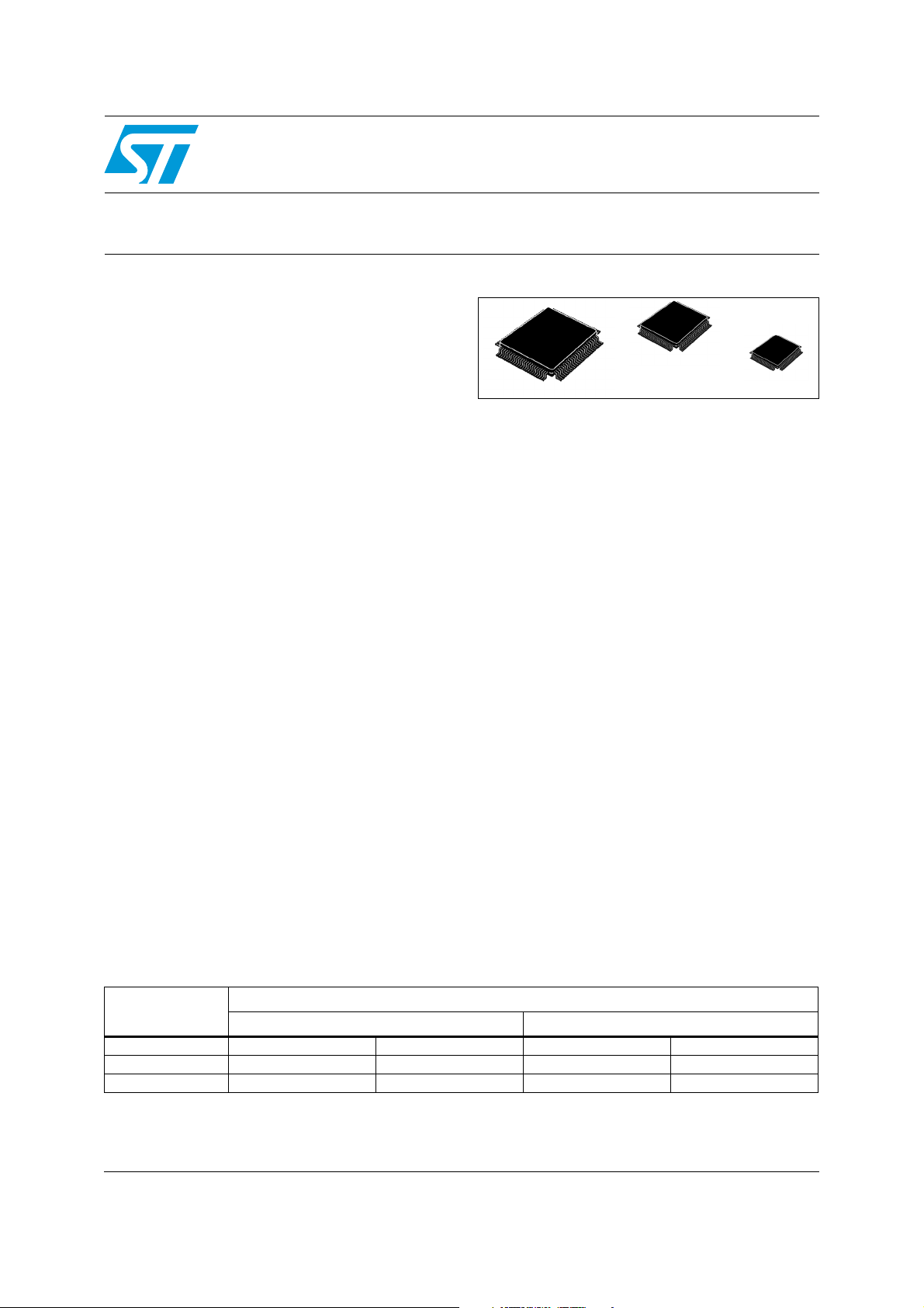
■ GPIO: LQFP64/45, LQFP100/75,
LQFP144/123
■ Timer units
– 6-channel 32-bit periodic interrupt timers
– 4-channel 32-bit system timer module
– System watchdog timer
– Real-time clock timer
■ 16-bit counter time-triggered I/Os
– Up to 56 channels with PWM/MC/IC/OC
– ADC diagnostic via CTU
■ Communications interface
– Up to 6 FlexCAN interfaces (2.0B active)
with 64-message objects each
– Up to 4 LINFlex/UART
– 3 DSPI / I
2
C
LQFP100 (14 x 14 x 1.4 mm)
LQFP144 (20 x 20 x 1.4 mm)
■ 10-bit A/D converter with up to 36 channels
LQFP64 (10 x 10 x 1.4 mm)
– Up to 64 channels via external multiplexing
– Individual conversion registers
– Cross triggering unit
■ Dedicated diagnostic module for lighting
– Advanced PWM generation
– Time-triggered diagnostic
– PWM-synchronized ADC measurements
■ Clock generation
– 4 to 16 MHz fast external crystal oscillator
– 32 KHz slow external crystal oscillator
– 16 MHz fast internal RC oscillator
– 128 kHz slow internal RC oscillator
– Software-controlled FMPLL
– Clock monitoring unit
■ Exhaustive debugging capability
– Nexus1 on all devices
– Nexus2+ available on emulation package
■ Low power capabilities
– Ultra-low power standby with RTC, SRAM
and CAN monitoring
– Fast wakeup schemes
■ Operating temp. range up to -40 to 125 °C
■ Single 5 V or 3.3 V supply
Table 1. Device summary
Package
LQFP144 SPC560B40L5 — SPC560B50L5 —
LQFP100 SPC560B40L3 SPC560C40L3 SPC560B50L3 SPC560C50L3
LQFP64
1. All LQFP64 information is indicative and must be confirmed during silicon validation.
October 2011 Doc ID 14619 Rev 9 1/117
(1)
256 KB code Flash memory 512 KB code Flash memory
SPC560B40L1 SPC560C40L1 SPC560B50L1 SPC560C50L1
Part number
www.st.com
1

Contents SPC560B40x/50x, SPC560C40x/50x
Contents
1 Introduction . . . . . . . . . . . . . . . . . . . . . . . . . . . . . . . . . . . . . . . . . . . . . . . . 8
1.1 Document overview . . . . . . . . . . . . . . . . . . . . . . . . . . . . . . . . . . . . . . . . . . 8
1.2 Description . . . . . . . . . . . . . . . . . . . . . . . . . . . . . . . . . . . . . . . . . . . . . . . . . 8
2 Block diagram . . . . . . . . . . . . . . . . . . . . . . . . . . . . . . . . . . . . . . . . . . . . . 11
3 Package pinouts and signal descriptions . . . . . . . . . . . . . . . . . . . . . . . 14
3.1 Package pinouts . . . . . . . . . . . . . . . . . . . . . . . . . . . . . . . . . . . . . . . . . . . . 14
3.2 Pad configuration during reset phases . . . . . . . . . . . . . . . . . . . . . . . . . . . 17
3.3 Voltage supply pins . . . . . . . . . . . . . . . . . . . . . . . . . . . . . . . . . . . . . . . . . 18
3.4 Pad types . . . . . . . . . . . . . . . . . . . . . . . . . . . . . . . . . . . . . . . . . . . . . . . . . 19
3.5 System pins . . . . . . . . . . . . . . . . . . . . . . . . . . . . . . . . . . . . . . . . . . . . . . . 19
3.6 Functional ports . . . . . . . . . . . . . . . . . . . . . . . . . . . . . . . . . . . . . . . . . . . . 20
3.7 Nexus 2+ pins . . . . . . . . . . . . . . . . . . . . . . . . . . . . . . . . . . . . . . . . . . . . . . 42
4 Electrical characteristics . . . . . . . . . . . . . . . . . . . . . . . . . . . . . . . . . . . . 43
4.1 Introduction . . . . . . . . . . . . . . . . . . . . . . . . . . . . . . . . . . . . . . . . . . . . . . . 43
4.2 Parameter classification . . . . . . . . . . . . . . . . . . . . . . . . . . . . . . . . . . . . . . 43
4.3 NVUSRO register . . . . . . . . . . . . . . . . . . . . . . . . . . . . . . . . . . . . . . . . . . . 44
4.3.1 NVUSRO[PAD3V5V] field description . . . . . . . . . . . . . . . . . . . . . . . . . . 44
4.3.2 NVUSRO[OSCILLATOR_MARGIN] field description . . . . . . . . . . . . . . . 44
4.3.3 NVUSRO[WATCHDOG_EN] field description . . . . . . . . . . . . . . . . . . . . 44
4.4 Absolute maximum ratings . . . . . . . . . . . . . . . . . . . . . . . . . . . . . . . . . . . . 45
4.5 Recommended operating conditions . . . . . . . . . . . . . . . . . . . . . . . . . . . . 46
4.6 Thermal characteristics . . . . . . . . . . . . . . . . . . . . . . . . . . . . . . . . . . . . . . 48
4.6.1 Package thermal characteristics . . . . . . . . . . . . . . . . . . . . . . . . . . . . . . 48
4.6.2 Power considerations . . . . . . . . . . . . . . . . . . . . . . . . . . . . . . . . . . . . . . . 49
4.7 I/O pad electrical characteristics . . . . . . . . . . . . . . . . . . . . . . . . . . . . . . . 50
4.7.1 I/O pad types . . . . . . . . . . . . . . . . . . . . . . . . . . . . . . . . . . . . . . . . . . . . . 50
4.7.2 I/O input DC characteristics . . . . . . . . . . . . . . . . . . . . . . . . . . . . . . . . . . 50
4.7.3 I/O output DC characteristics . . . . . . . . . . . . . . . . . . . . . . . . . . . . . . . . . 51
4.7.4 Output pin transition times . . . . . . . . . . . . . . . . . . . . . . . . . . . . . . . . . . . 54
4.7.5 I/O pad current specification . . . . . . . . . . . . . . . . . . . . . . . . . . . . . . . . . 54
2/117 Doc ID 14619 Rev 9

SPC560B40x/50x, SPC560C40x/50x Contents
4.8 RESET electrical characteristics . . . . . . . . . . . . . . . . . . . . . . . . . . . . . . . 60
4.9 Power management electrical characteristics . . . . . . . . . . . . . . . . . . . . . 63
4.9.1 Voltage regulator electrical characteristics . . . . . . . . . . . . . . . . . . . . . . 63
4.9.2 Low voltage detector electrical characteristics . . . . . . . . . . . . . . . . . . . . 68
4.10 Power consumption . . . . . . . . . . . . . . . . . . . . . . . . . . . . . . . . . . . . . . . . . 69
4.11 Flash memory electrical characteristics . . . . . . . . . . . . . . . . . . . . . . . . . . 70
4.11.1 Program/Erase characteristics . . . . . . . . . . . . . . . . . . . . . . . . . . . . . . . . 70
4.11.2 Flash power supply DC characteristics . . . . . . . . . . . . . . . . . . . . . . . . . 72
4.11.3 Start-up/Switch-off timings . . . . . . . . . . . . . . . . . . . . . . . . . . . . . . . . . . . 73
4.12 Electromagnetic compatibility (EMC) characteristics . . . . . . . . . . . . . . . . 73
4.12.1 Designing hardened software to avoid noise problems . . . . . . . . . . . . . 73
4.12.2 Electromagnetic interference (EMI) . . . . . . . . . . . . . . . . . . . . . . . . . . . . 74
4.12.3 Absolute maximum ratings (electrical sensitivity) . . . . . . . . . . . . . . . . . 74
4.13 Fast external crystal oscillator (4 to 16 MHz) electrical characteristics . . 75
4.14 Slow external crystal oscillator (32 kHz) electrical characteristics . . . . . . 78
4.15 FMPLL electrical characteristics . . . . . . . . . . . . . . . . . . . . . . . . . . . . . . . 80
4.16 Fast internal RC oscillator (16 MHz) electrical characteristics . . . . . . . . . 81
4.17 Slow internal RC oscillator (128 kHz) electrical characteristics . . . . . . . . 82
4.18 ADC electrical characteristics . . . . . . . . . . . . . . . . . . . . . . . . . . . . . . . . . 83
4.18.1 Introduction . . . . . . . . . . . . . . . . . . . . . . . . . . . . . . . . . . . . . . . . . . . . . . 83
4.18.2 Input impedance and ADC accuracy . . . . . . . . . . . . . . . . . . . . . . . . . . . 83
4.18.3 ADC electrical characteristics . . . . . . . . . . . . . . . . . . . . . . . . . . . . . . . . 88
4.19 On-chip peripherals . . . . . . . . . . . . . . . . . . . . . . . . . . . . . . . . . . . . . . . . . 90
4.19.1 Current consumption . . . . . . . . . . . . . . . . . . . . . . . . . . . . . . . . . . . . . . . 90
4.19.2 DSPI characteristics . . . . . . . . . . . . . . . . . . . . . . . . . . . . . . . . . . . . . . . 92
4.19.3 Nexus characteristics . . . . . . . . . . . . . . . . . . . . . . . . . . . . . . . . . . . . . . . 98
4.19.4 JTAG characteristics . . . . . . . . . . . . . . . . . . . . . . . . . . . . . . . . . . . . . . 100
5 Package characteristics . . . . . . . . . . . . . . . . . . . . . . . . . . . . . . . . . . . . 101
5.1 ECOPACK
5.2 Package mechanical data . . . . . . . . . . . . . . . . . . . . . . . . . . . . . . . . . . . 101
5.2.1 LQFP64 . . . . . . . . . . . . . . . . . . . . . . . . . . . . . . . . . . . . . . . . . . . . . . . . 101
® . . . . . . . . . . . . . . . . . . . . . . . . . . . . . . . . . . . . . . . . . . . . . . . . . . . . . . . . . . . 101
5.2.2 LQFP100 . . . . . . . . . . . . . . . . . . . . . . . . . . . . . . . . . . . . . . . . . . . . . . . 103
5.2.3 LQFP144 . . . . . . . . . . . . . . . . . . . . . . . . . . . . . . . . . . . . . . . . . . . . . . . 104
5.2.4 LBGA208 . . . . . . . . . . . . . . . . . . . . . . . . . . . . . . . . . . . . . . . . . . . . . . . 106
Doc ID 14619 Rev 9 3/117

Contents SPC560B40x/50x, SPC560C40x/50x
6 Ordering information . . . . . . . . . . . . . . . . . . . . . . . . . . . . . . . . . . . . . . 108
Appendix A Abbreviations. . . . . . . . . . . . . . . . . . . . . . . . . . . . . . . . . . . . . . . . . . 109
Revision history . . . . . . . . . . . . . . . . . . . . . . . . . . . . . . . . . . . . . . . . . . . . . . . . . . . 110
4/117 Doc ID 14619 Rev 9

SPC560B40x/50x, SPC560C40x/50x List of tables
List of tables
Table 1. Device summary . . . . . . . . . . . . . . . . . . . . . . . . . . . . . . . . . . . . . . . . . . . . . . . . . . . . . . . . . . 1
Table 2. SPC560B40x/50x and SPC560C40x/50x device comparison . . . . . . . . . . . . . . . . . . . . . . . 9
Table 3. SPC560B40x/50x and SPC560C40x/50x series block summary . . . . . . . . . . . . . . . . . . . . 12
Table 4. Voltage supply pin descriptions . . . . . . . . . . . . . . . . . . . . . . . . . . . . . . . . . . . . . . . . . . . . . 18
Table 5. System pin descriptions . . . . . . . . . . . . . . . . . . . . . . . . . . . . . . . . . . . . . . . . . . . . . . . . . . . 19
Table 6. Functional port pin descriptions . . . . . . . . . . . . . . . . . . . . . . . . . . . . . . . . . . . . . . . . . . . . . 20
Table 7. Nexus 2+ pin descriptions. . . . . . . . . . . . . . . . . . . . . . . . . . . . . . . . . . . . . . . . . . . . . . . . . . 42
Table 8. Parameter classifications . . . . . . . . . . . . . . . . . . . . . . . . . . . . . . . . . . . . . . . . . . . . . . . . . . 43
Table 9. PAD3V5V field description . . . . . . . . . . . . . . . . . . . . . . . . . . . . . . . . . . . . . . . . . . . . . . . . . 44
Table 10. OSCILLATOR_MARGIN field description. . . . . . . . . . . . . . . . . . . . . . . . . . . . . . . . . . . . . . 44
Table 11. WATCHDOG_EN field description . . . . . . . . . . . . . . . . . . . . . . . . . . . . . . . . . . . . . . . . . . . 44
Table 12. Absolute maximum ratings . . . . . . . . . . . . . . . . . . . . . . . . . . . . . . . . . . . . . . . . . . . . . . . . . 45
Table 13. Recommended operating conditions (3.3 V) . . . . . . . . . . . . . . . . . . . . . . . . . . . . . . . . . . . 46
Table 14. Recommended operating conditions (5.0 V) . . . . . . . . . . . . . . . . . . . . . . . . . . . . . . . . . . . 46
Table 15. LQFP thermal characteristics . . . . . . . . . . . . . . . . . . . . . . . . . . . . . . . . . . . . . . . . . . . . . . . 48
Table 16. I/O input DC electrical characteristics . . . . . . . . . . . . . . . . . . . . . . . . . . . . . . . . . . . . . . . . . 51
Table 17. I/O pull-up/pull-down DC electrical characteristics . . . . . . . . . . . . . . . . . . . . . . . . . . . . . . . 51
Table 18. SLOW configuration output buffer electrical characteristics . . . . . . . . . . . . . . . . . . . . . . . . 52
Table 19. MEDIUM configuration output buffer electrical characteristics . . . . . . . . . . . . . . . . . . . . . . 52
Table 20. FAST configuration output buffer electrical characteristics. . . . . . . . . . . . . . . . . . . . . . . . . 53
Table 21. Output pin transition times . . . . . . . . . . . . . . . . . . . . . . . . . . . . . . . . . . . . . . . . . . . . . . . . . 54
Table 22. I/O supply segment . . . . . . . . . . . . . . . . . . . . . . . . . . . . . . . . . . . . . . . . . . . . . . . . . . . . . . . 54
Table 23. I/O consumption . . . . . . . . . . . . . . . . . . . . . . . . . . . . . . . . . . . . . . . . . . . . . . . . . . . . . . . . . 55
Table 24. I/O weight . . . . . . . . . . . . . . . . . . . . . . . . . . . . . . . . . . . . . . . . . . . . . . . . . . . . . . . . . . . . . . 56
Table 25. Reset electrical characteristics . . . . . . . . . . . . . . . . . . . . . . . . . . . . . . . . . . . . . . . . . . . . . . 61
Table 26. Voltage regulator electrical characteristics . . . . . . . . . . . . . . . . . . . . . . . . . . . . . . . . . . . . . 66
Table 27. Low voltage detector electrical characteristics . . . . . . . . . . . . . . . . . . . . . . . . . . . . . . . . . . 69
Table 28. Power consumption on VDD_BV and VDD_HV . . . . . . . . . . . . . . . . . . . . . . . . . . . . . . . . . 69
Table 29. Program and erase specifications . . . . . . . . . . . . . . . . . . . . . . . . . . . . . . . . . . . . . . . . . . . 71
Table 30. Flash module life. . . . . . . . . . . . . . . . . . . . . . . . . . . . . . . . . . . . . . . . . . . . . . . . . . . . . . . . . 71
Table 31. Flash read access timing . . . . . . . . . . . . . . . . . . . . . . . . . . . . . . . . . . . . . . . . . . . . . . . . . . 71
Table 32. Flash memory power supply DC electrical characteristics . . . . . . . . . . . . . . . . . . . . . . . . . 72
Table 33. Start-up time/Switch-off time. . . . . . . . . . . . . . . . . . . . . . . . . . . . . . . . . . . . . . . . . . . . . . . . 73
Table 34. EMI radiated emission measurement . . . . . . . . . . . . . . . . . . . . . . . . . . . . . . . . . . . . . . . . . 74
Table 35. ESD absolute maximum ratings . . . . . . . . . . . . . . . . . . . . . . . . . . . . . . . . . . . . . . . . . . . . 74
Table 36. Latch-up results . . . . . . . . . . . . . . . . . . . . . . . . . . . . . . . . . . . . . . . . . . . . . . . . . . . . . . . . . 75
Table 37. Crystal description . . . . . . . . . . . . . . . . . . . . . . . . . . . . . . . . . . . . . . . . . . . . . . . . . . . . . . . 76
Table 38. Fast external crystal oscillator (4 to 16 MHz) electrical characteristics. . . . . . . . . . . . . . . . 77
Table 39. Crystal motional characteristics . . . . . . . . . . . . . . . . . . . . . . . . . . . . . . . . . . . . . . . . . . . . . 79
Table 40. Slow external crystal oscillator (32 kHz) electrical characteristics . . . . . . . . . . . . . . . . . . . 80
Table 41. FMPLL electrical characteristics . . . . . . . . . . . . . . . . . . . . . . . . . . . . . . . . . . . . . . . . . . . . . 80
Table 42. Fast internal RC oscillator (16 MHz) electrical characteristics . . . . . . . . . . . . . . . . . . . . . . 81
Table 43. Slow internal RC oscillator (128 kHz) electrical characteristics . . . . . . . . . . . . . . . . . . . . . 82
Table 44. ADC input leakage current . . . . . . . . . . . . . . . . . . . . . . . . . . . . . . . . . . . . . . . . . . . . . . . . . 88
Table 45. ADC conversion characteristics . . . . . . . . . . . . . . . . . . . . . . . . . . . . . . . . . . . . . . . . . . . . . 89
Table 46. On-chip peripherals current consumption . . . . . . . . . . . . . . . . . . . . . . . . . . . . . . . . . . . . . . 91
Table 47. DSPI characteristics . . . . . . . . . . . . . . . . . . . . . . . . . . . . . . . . . . . . . . . . . . . . . . . . . . . . . . 92
Table 48. Nexus characteristics . . . . . . . . . . . . . . . . . . . . . . . . . . . . . . . . . . . . . . . . . . . . . . . . . . . . . 98
Doc ID 14619 Rev 9 5/117

List of tables SPC560B40x/50x, SPC560C40x/50x
Table 49. JTAG characteristics. . . . . . . . . . . . . . . . . . . . . . . . . . . . . . . . . . . . . . . . . . . . . . . . . . . . . 100
Table 50. LQFP64 mechanical data . . . . . . . . . . . . . . . . . . . . . . . . . . . . . . . . . . . . . . . . . . . . . . . . . 101
Table 51. LQFP100 mechanical data . . . . . . . . . . . . . . . . . . . . . . . . . . . . . . . . . . . . . . . . . . . . . . . . 103
Table 52. LQFP144 mechanical data . . . . . . . . . . . . . . . . . . . . . . . . . . . . . . . . . . . . . . . . . . . . . . . . 105
Table 53. LBGA208 mechanical data . . . . . . . . . . . . . . . . . . . . . . . . . . . . . . . . . . . . . . . . . . . . . . . . 106
Table 54. Abbreviations . . . . . . . . . . . . . . . . . . . . . . . . . . . . . . . . . . . . . . . . . . . . . . . . . . . . . . . . . . 109
Table 55. Document revision history . . . . . . . . . . . . . . . . . . . . . . . . . . . . . . . . . . . . . . . . . . . . . . . . 110
6/117 Doc ID 14619 Rev 9

SPC560B40x/50x, SPC560C40x/50x List of figures
List of figures
Figure 1. SPC560B40x/50x and SPC560C40x/50x block diagram . . . . . . . . . . . . . . . . . . . . . . . . . . 11
Figure 2. LQFP 64-pin configuration . . . . . . . . . . . . . . . . . . . . . . . . . . . . . . . . . . . . . . . . . . . . . . . . . 14
Figure 3. LQFP 100-pin configuration . . . . . . . . . . . . . . . . . . . . . . . . . . . . . . . . . . . . . . . . . . . . . . . . 15
Figure 4. LQFP 144-pin configuration . . . . . . . . . . . . . . . . . . . . . . . . . . . . . . . . . . . . . . . . . . . . . . . . 16
Figure 5. LBGA208 confguration . . . . . . . . . . . . . . . . . . . . . . . . . . . . . . . . . . . . . . . . . . . . . . . . . . . . 17
Figure 6. I/O input DC electrical characteristics definition . . . . . . . . . . . . . . . . . . . . . . . . . . . . . . . . . 50
Figure 7. Start-up reset requirements . . . . . . . . . . . . . . . . . . . . . . . . . . . . . . . . . . . . . . . . . . . . . . . . 61
Figure 8. Noise filtering on reset signal . . . . . . . . . . . . . . . . . . . . . . . . . . . . . . . . . . . . . . . . . . . . . . . 61
Figure 9. Voltage regulator capacitance connection . . . . . . . . . . . . . . . . . . . . . . . . . . . . . . . . . . . . . 64
Figure 10. VDD and VDD_BV maximum slope . . . . . . . . . . . . . . . . . . . . . . . . . . . . . . . . . . . . . . . . . . 65
Figure 11. VDD and VDD_BV supply constraints during STANDBY mode exit. . . . . . . . . . . . . . . . . . 65
Figure 12. Low voltage detector vs reset . . . . . . . . . . . . . . . . . . . . . . . . . . . . . . . . . . . . . . . . . . . . . . . 68
Figure 13. Crystal oscillator and resonator connection scheme . . . . . . . . . . . . . . . . . . . . . . . . . . . . . 76
Figure 14. Fast external crystal oscillator (4 to 16 MHz) timing diagram . . . . . . . . . . . . . . . . . . . . . . . 77
Figure 15. Crystal oscillator and resonator connection scheme . . . . . . . . . . . . . . . . . . . . . . . . . . . . . 78
Figure 16. Equivalent circuit of a quartz crystal . . . . . . . . . . . . . . . . . . . . . . . . . . . . . . . . . . . . . . . . . . 79
Figure 17. Slow external crystal oscillator (32 kHz) timing diagram. . . . . . . . . . . . . . . . . . . . . . . . . . . 80
Figure 18. ADC characteristic and error definitions . . . . . . . . . . . . . . . . . . . . . . . . . . . . . . . . . . . . . . . 83
Figure 19. Input equivalent circuit (precise channels) . . . . . . . . . . . . . . . . . . . . . . . . . . . . . . . . . . . . . 85
Figure 20. Input equivalent circuit (extended channels) . . . . . . . . . . . . . . . . . . . . . . . . . . . . . . . . . . . 85
Figure 21. Transient behavior during sampling phase . . . . . . . . . . . . . . . . . . . . . . . . . . . . . . . . . . . . . 86
Figure 22. Spectral representation of input signal . . . . . . . . . . . . . . . . . . . . . . . . . . . . . . . . . . . . . . . . 87
Figure 23. DSPI classic SPI timing – master, CPHA = 0 . . . . . . . . . . . . . . . . . . . . . . . . . . . . . . . . . . . 94
Figure 24. DSPI classic SPI timing – master, CPHA = 1 . . . . . . . . . . . . . . . . . . . . . . . . . . . . . . . . . . . 95
Figure 25. DSPI classic SPI timing – slave, CPHA = 0 . . . . . . . . . . . . . . . . . . . . . . . . . . . . . . . . . . . . 95
Figure 26. DSPI classic SPI timing – slave, CPHA = 1 . . . . . . . . . . . . . . . . . . . . . . . . . . . . . . . . . . . . 96
Figure 27. DSPI modified transfer format timing – master, CPHA = 0 . . . . . . . . . . . . . . . . . . . . . . . . . 96
Figure 28. DSPI modified transfer format timing – master, CPHA = 1 . . . . . . . . . . . . . . . . . . . . . . . . . 97
Figure 29. DSPI modified transfer format timing – slave, CPHA = 0 . . . . . . . . . . . . . . . . . . . . . . . . . . 97
Figure 30. DSPI modified transfer format timing – slave, CPHA = 1 . . . . . . . . . . . . . . . . . . . . . . . . . . 98
Figure 31. DSPI PCS strobe (PCSS) timing . . . . . . . . . . . . . . . . . . . . . . . . . . . . . . . . . . . . . . . . . . . . 98
Figure 32. Nexus TDI, TMS, TDO timing . . . . . . . . . . . . . . . . . . . . . . . . . . . . . . . . . . . . . . . . . . . . . . . 99
Figure 33. Timing diagram – JTAG boundary scan . . . . . . . . . . . . . . . . . . . . . . . . . . . . . . . . . . . . . . 100
Figure 34. LQFP64 package mechanical drawing . . . . . . . . . . . . . . . . . . . . . . . . . . . . . . . . . . . . . . . 101
Figure 35. LQFP100 package mechanical drawing . . . . . . . . . . . . . . . . . . . . . . . . . . . . . . . . . . . . . . 103
Figure 36. LQFP144 package mechanical drawing . . . . . . . . . . . . . . . . . . . . . . . . . . . . . . . . . . . . . . 104
Figure 37. LBGA208 package mechanical drawing . . . . . . . . . . . . . . . . . . . . . . . . . . . . . . . . . . . . . . 106
Figure 38. Ordering information scheme . . . . . . . . . . . . . . . . . . . . . . . . . . . . . . . . . . . . . . . . . . . . . . 108
Doc ID 14619 Rev 9 7/117

Introduction SPC560B40x/50x, SPC560C40x/50x
1 Introduction
1.1 Document overview
This document describes the features of the family and options available within the family
members, and highlights important electrical and physical characteristics of the device. To
ensure a complete understanding of the device functionality, refer also to the device
reference manual and errata sheet.
1.2 Description
The SPC560B40x/50x and SPC560C40x/50x is a family of next generation microcontrollers
built on the Power Architecture embedded category.
The SPC560B40x/50x and SPC560C40x/50x family of 32-bit microcontrollers is the latest
achievement in integrated automotive application controllers. It belongs to an expanding
family of automotive-focused products designed to address the next wave of body
electronics applications within the vehicle. The advanced and cost-efficient host processor
core of this automotive controller family complies with the Power Architecture embedded
category and only implements the VLE (variable-length encoding) APU, providing improved
code density. It operates at speeds of up to 64 MHz and offers high performance processing
optimized for low power consumption. It capitalizes on the available development
infrastructure of current Power Architecture devices and is supported with software drivers,
operating systems and configuration code to assist with users implementations.
8/117 Doc ID 14619 Rev 9
Table 2. SPC560B40x/50x and SPC560C40x/50x device comparison
SPC560B40x/50x, SPC560C40x/50x Introduction
(1)
Device
Doc ID 14619 Rev 9 9/117
Feature
SPC560B
40L1
SPC560B
40L3
SPC560B
40L5
SPC560C
40L1
SPC560C
40L3
SPC560B
50L1
SPC560B
50L3
SPC560B
50L5
SPC560C
50L1
SPC560C
50L3
SPC560B
50B2
CPU e200z0h
Execution
(2)
speed
Static – up to 64 MHz
Code Flash 256 KB 512 KB
Data Flash 64 KB (4 × 16 KB)
RAM 24KB 32KB 32KB 48 KB
MPU 8-entry
ADC (10-bit) 12 ch 28 ch 36 ch 8 ch 28 ch 12 ch 28 ch 36 ch 8 ch 28 ch 36 ch
CTU Ye s
(3)
Total timer I/O
eMIOS
– PWM + MC +
– PWM +
–IC/OC
IC/OC
IC/OC
(4)
(4)
(4)
12 ch,
16-bit
2 ch 5 ch 10 ch 2 ch 5 ch 2 ch 5 ch 10 ch 2 ch 5 ch 10 ch
10 ch 20 ch 40 ch 10 ch 20 ch 10 ch 20 ch 40 ch 10 ch 20 ch 40 ch
— 3 ch 6 ch — 3 ch — 3 ch 6 ch — 3 ch 6 ch
SCI (LINFlex) 3
28 ch,
16-bit
(5)
56 ch,
16-bit
12 ch,
16-bit
28 ch,
16-bit
12 ch,
16-bit
28 ch,
16-bit
4
56 ch,
16-bit
12 ch,
16-bit
28 ch,
16-bit
56 ch,
16-bit
SPI (DSPI) 2 3 2 3 2 3 2 3
CAN (FlexCAN) 2
2
C 1
I
(6)
56 3
(7)
56
32 kHz oscillator Yes
(8)
GPIO
45 79 123 45 79 45 79 123 45 79 123
10/117 Doc ID 14619 Rev 9
Table 2. SPC560B40x/50x and SPC560C40x/50x device comparison
(1)
(continued)
Device
Introduction SPC560B40x/50x, SPC560C40x/50x
Feature
SPC560B
40L1
SPC560B
40L3
SPC560B
40L5
SPC560C
40L1
SPC560C
40L3
SPC560B
50L1
SPC560B
50L3
SPC560B
50L5
SPC560C
50L1
SPC560C
50L3
SPC560B
50B2
Debug JTAG Nexus2+
Package LQFP64
1. Feature set dependent on selected peripheral multiplexing—table shows example implementation
2. Based on 125 °C ambient operating temperature
3. See the eMIOS section of the device reference manual for information on the channel configuration and functions.
4. IC – Input Capture; OC – Output Compare; PWM – Pulse Width Modulation; MC – Modulus counter
5. SCI0, SCI1 and SCI2 are available. SCI3 is not available.
6. CAN0, CAN1 are available. CAN2, CAN3, CAN4 and CAN5 are not available.
7. CAN0, CAN1 and CAN2 are available. CAN3, CAN4 and CAN5 are not available.
8. I/O count based on multiplexing with peripherals
9. All LQFP64 information is indicative and must be confirmed during silicon validation.
10. LBGA208 available only as development package for Nexus2+
(9)
LQFP100 LQFP144 LQFP64
(9)
LQFP100 LQFP64
(9)
LQFP100 LQFP144 LQFP64
(9)
LQFP100
LBGA208
(10)
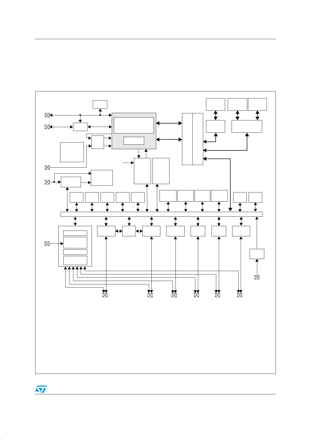
SPC560B40x/50x, SPC560C40x/50x Block diagram
2 Block diagram
Figure 1 shows a top-level block diagram of the SPC560B40x/50x and SPC560C40x/50x
device series.
Figure 1. SPC560B40x/50x and SPC560C40x/50x block diagram
JTAG port
Nexus port
NMI
Clocks
Interrupt
request
Nexus
Vol ta ge
regulator
FMPLL
RTC
SIUL
Reset control
External
interrupt
request
IMUX
GPIO and
pad control
JTAG
NMI
SIUL
Interrupt requests
from peripheral
blocks
CMU
SWT
36 Ch.
ADC
ECSM
e200z0h
Nexus 2+
CTU
PITSTM
INTC
eMIOS
Instructions
(Master)
Data
(Master)
MPU
registers
Peripheral bridge
2 x
4 x
LINFlex
64-bit 2 x 3 Crossbar Switch
3 x
DSPI
MPU
SRAM
48 KB
SRAM
controller
(Slave)
MC_PCUMC_MEMC_CGMMC_RGM
I2C
Code Flash
512 KB
controller
(Slave)
BAM
6 x
FlexCAN
Data Flash
64 KB
Flash
(Slave)
SSCM
WKPU
I/O
Legend:
ADC Analog-to-Digital Converter
BAM Boot Assist Module
FlexCAN Controller Area Network
CMU Clock Monitor Unit
CTU Cross Triggering Unit
DSPI Deserial Serial Peripheral Interface
eMIOS Enhanced Modular Input Output System
FMPLL Frequency-Modulated Phase-Locked Loop
2
C Inter-integrated Circuit Bus
I
IMUX Internal Multiplexer
INTC Interrupt Controller
JTAG JTAG controller
LINFlex Serial Communication Interface (LIN support)
ECSM Error Correction Status Module
. . .
Doc ID 14619 Rev 9 11/117
. . .
MC_CGM Clock Generation Module
MC_ME Mode Entry Module
MC_PCU Power Control Unit
MC_RGM Reset Generation Module
MPU Memory Protection Unit
Nexus Nexus Development Interface (NDI) Level
NMI Non-Maskable Interrupt
PIT Periodic Interrupt Timer
RTC Real-Time Clock
SIUL System Integration Unit Lite
SRAM Static Random-Access Memory
SSCM System Status Configuration Module
STM System Timer Module
SWT Software Watchdog Timer
WKPU Wakeup Unit
. . .
. . .
. . .
Interrupt
request with
wakeup
functionality
Block diagram SPC560B40x/50x, SPC560C40x/50x
Ta bl e 3 summarizes the functions of all blocks present in the SPC560B40x/50x and
SPC560C40x/50x series of microcontrollers. Please note that the presence and number of
blocks vary by device and package.
Table 3. SPC560B40x/50x and SPC560C40x/50x series block summary
Analog-to-digital converter (ADC) Multi-channel, 10-bit analog-to-digital converter
Boot assist module (BAM)
Clock monitor unit (CMU) Monitors clock source (internal and external) integrity
Cross triggering unit (CTU)
Deserial serial peripheral
interface (DSPI)
Error Correction Status Module
(ECSM)
Enhanced Direct Memory Access
(eDMA)
Enhanced modular input output
system (eMIOS)
Block Function
A block of read-only memory containing VLE code which is executed according
to the boot mode of the device
Enables synchronization of ADC conversions with a timer event from the eMIOS
or from the PIT
Provides a synchronous serial interface for communication with external
devices
Provides a myriad of miscellaneous control functions for the device including
program-visible information about configuration and revision levels, a reset
status register, wakeup control for exiting sleep modes, and optional features
such as information on memory errors reported by error-correcting codes
Performs complex data transfers with minimal intervention from a host
processor via “n” programmable channels.
Provides the functionality to generate or measure events
Flash memory Provides non-volatile storage for program code, constants and variables
FlexCAN (controller area
network)
Frequency-modulated phaselocked loop (FMPLL)
Internal multiplexer (IMUX) SIU
subblock
2
Inter-integrated circuit (I
C™) bus
Supports the standard CAN communications protocol
Generates high-speed system clocks and supports programmable frequency
modulation
Allows flexible mapping of peripheral interface on the different pins of the device
A two wire bidirectional serial bus that provides a simple and efficient method of
data exchange between devices
Interrupt controller (INTC) Provides priority-based preemptive scheduling of interrupt requests
JTAG controller
LINFlex controller
Clock generation module
(MC_CGM)
Provides the means to test chip functionality and connectivity while remaining
transparent to system logic when not in test mode
Manages a high number of LIN (Local Interconnect Network protocol)
messages efficiently with a minimum of CPU load
Provides logic and control required for the generation of system and peripheral
clocks
Provides a mechanism for controlling the device operational mode and mode
Mode entry module (MC_ME)
transition sequences in all functional states; also manages the power control
unit, reset generation module and clock generation module, and holds the
configuration, control and status registers accessible for applications
12/117 Doc ID 14619 Rev 9

SPC560B40x/50x, SPC560C40x/50x Block diagram
Table 3. SPC560B40x/50x and SPC560C40x/50x series block summary (continued)
Block Function
Reduces the overall power consumption by disconnecting parts of the device
Power control unit (MC_PCU)
Reset generation module
(MC_RGM)
Memory protection unit (MPU)
from the power supply via a power switching device; device components are
grouped into sections called “power domains” which are controlled by the PCU
Centralizes reset sources and manages the device reset sequence of the
device
Provides hardware access control for all memory references generated in a
device
Nexus development interface
(NDI)
Periodic interrupt timer (PIT) Produces periodic interrupts and triggers
Real-time counter (RTC)
System integration unit (SIU)
Static random-access memory
(SRAM)
System status configuration
module (SSCM)
System timer module (STM)
System watchdog timer (SWT) Provides protection from runaway code
Wakeup unit (WKPU)
Crossbar (XBAR) switch
Provides real-time development support capabilities in compliance with the
IEEE-ISTO 5001-2003 standard
A free running counter used for time keeping applications, the RTC can be
configured to generate an interrupt at a predefined interval independent of the
mode of operation (run mode or low-power mode)
Provides control over all the electrical pad controls and up 32 ports with 16 bits
of bidirectional, general-purpose input and output signals and supports up to 32
external interrupts with trigger event configuration
Provides storage for program code, constants, and variables
Provides system configuration and status data (such as memory size and
status, device mode and security status), device identification data, debug
status port enable and selection, and bus and peripheral abort enable/disable
Provides a set of output compare events to support AUTOSAR and operating
system tasks
The wakeup unit supports up to 18 external sources that can generate
interrupts or wakeup events, of which 1 can cause non-maskable interrupt
requests or wakeup events.
Supports simultaneous connections between two master ports and three slave
ports. The crossbar supports a 32-bit address bus width and a 64-bit data bus
width.
Doc ID 14619 Rev 9 13/117
Package pinouts and signal descriptions SPC560B40x/50x, SPC560C40x/50x
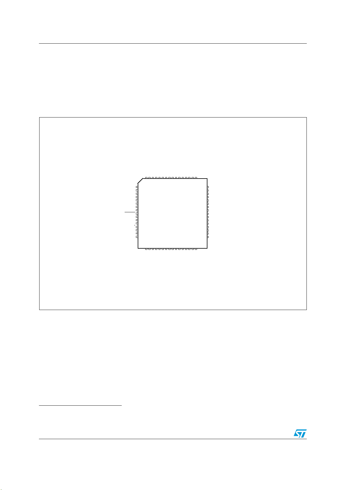
3 Package pinouts and signal descriptions
3.1 Package pinouts
The available LQFP pinouts and the LBGA208 ballmap are provided in the following figures.
For pin signal descriptions, please refer to the device reference manual (RM0017).
Figure 2. LQFP 64-pin configuration
PB[3]
1
PC[9]
2
PA[ 2 ]
3
PA[ 1 ]
4
PA[ 0 ]
5
VSS_HV
6
VDD_HV
7
VSS_HV
8
RESET
9
VSS_LV
10
VDD_LV
11
VDD_BV
12
PC[10]
13
PB[0]
14
PB[1]
15
PC[6]
16
(a)
PB[2]
PC[8]
PC[4]
PC[5]
PH[9]
PC[0]
VSS_LV
VDD_LV
VDD_HV
VSS_HV
PC[1]
PH[10]
PA[ 6 ]
646362616059585756555453525150
LQFP64 Top view
171819202122232425
PA[ 4 ]
PC[7]
PA[ 1 5 ]
PA[ 1 4 ]
PA[ 1 3 ]
PA[ 1 2 ]
VDD_LV
26272829303132
XTAL
EXTAL
VSS_LV
VSS_HV
PB[9]
VDD_HV
PA[ 5 ]
PC[2]
PC[3]
49
PA[ 1 1 ]
48
PA[ 1 0 ]
47
PA[ 9 ]
46
PA[ 8 ]
45
PA[ 7 ]
44
PA[ 3 ]
43
PB[15]
42
PB[14]
41
PB[13]
40
PB[12]
39
PB[11]
38
PB[7]
37
PB[6]
36
PB[5]
35
VDD_HV_ADC
34
VSS_HV_ADC
33
PB[8]
PB[4]
PB[10]
a. All LQFP64 information is indicative and must be confirmed during silicon validation.
14/117 Doc ID 14619 Rev 9
SPC560B40x/50x, SPC560C40x/50x Package pinouts and signal descriptions
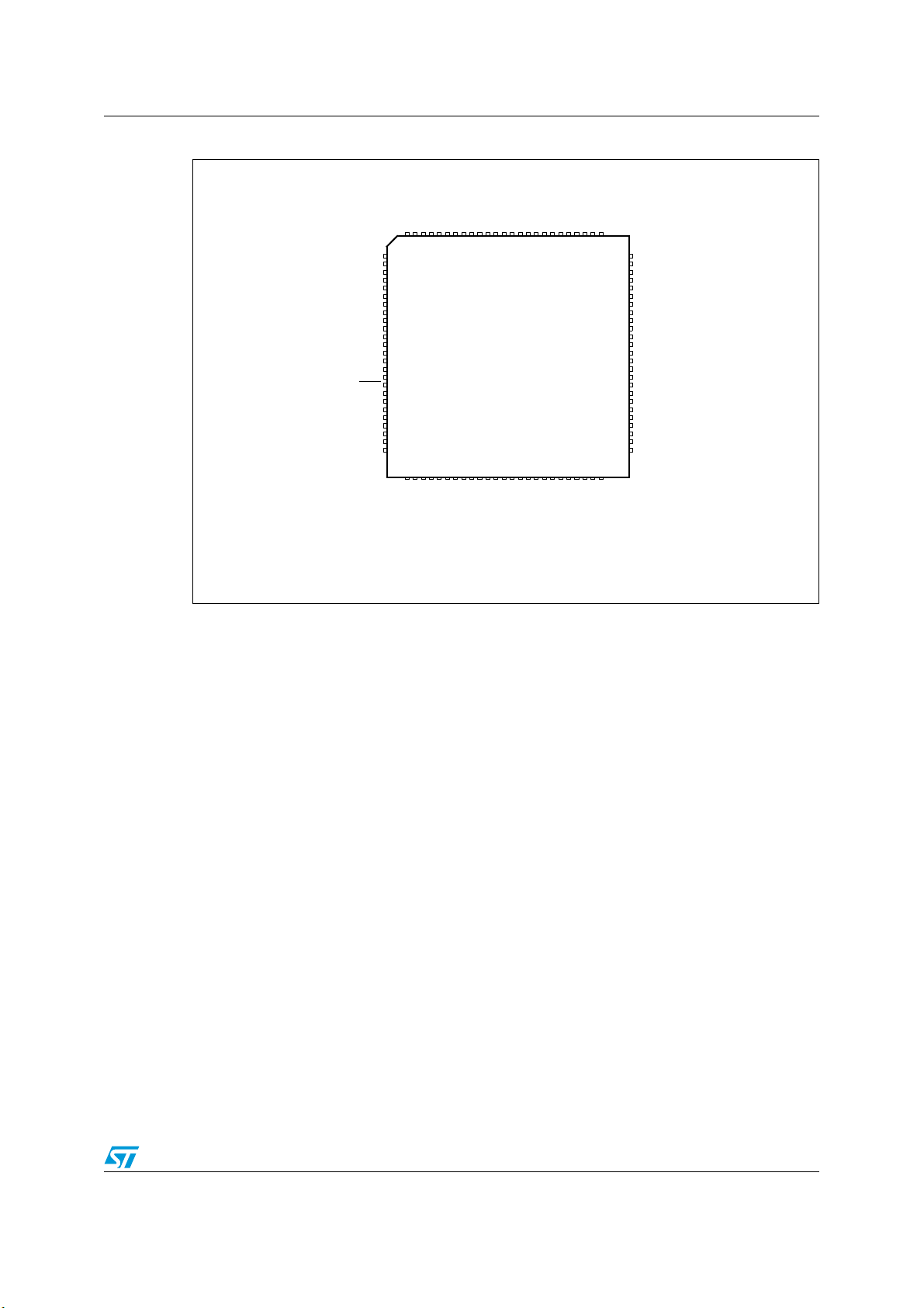
Figure 3. LQFP 100-pin configuration
PB[2]
PC[8]
PC[13]
PC[12]
PE[7]
PE[6]
PE[5]
PE[4]
PC[4]
PC[5]
PE[3]
PE[2]
PH[9]
PC[0]
VSS_LV
VDD_LV
VDD_HV
VSS_HV
PC[1]
PH[10]
PA[ 6 ]
PA[ 5 ]
PC[2]
PC[3]
PE[12]
PB[3]
PC[9]
PC[14]
PC[15]
PA[ 2 ]
PE[0]
PA[ 1 ]
PE[1]
PE[8]
PE[9]
PE[10]
PA[ 0 ]
PE[11]
VSS_HV
VDD_HV
VSS_HV
RESET
VSS_LV
VDD_LV
VDD_BV
PC[11]
PC[10]
PB[0]
PB[1]
PC[6]
9998979695949392919089888786858483828180797877
100
1
2
3
4
5
6
7
8
9
10
11
12
13
14
15
16
17
18
19
20
21
22
23
24
25
26272829303132333435363738394041424344454647484950
PC[7]
PA[ 1 5 ]
PA[ 1 4 ]
LQFP100
PA[ 4 ]
PA[ 1 3 ]
PA[ 1 2 ]
VDD_LV
Top view
XTAL
EXTAL
VSS_LV
VSS_HV
PB[9]
PB[8]
PD[0]
PD[1]
PD[2]
PD[3]
PB[10]
VDD_HV
76
PA[11]
75
PA[10]
74
PA[ 9 ]
73
PA[ 8 ]
72
PA[ 7 ]
71
VDD_HV
70
VSS_HV
69
PA[ 3 ]
68
PB[15]
67
PD[15]
66
PB[14]
65
PD[14]
64
PB[13]
63
PD[13]
62
PB[12]
61
PD[12]
60
PB[11]
59
PD[11]
58
PD[10]
57
PD[9]
56
PB[7]
55
PB[6]
54
PB[5]
53
VDD_HV_ADC
52
VSS_HV_ADC
51
PB[4]
PD[4]
PD[5]
PD[6]
PD[7]
PD[8]
Note:
Availability of port pin alternate functions depends on product selection.
Doc ID 14619 Rev 9 15/117
Package pinouts and signal descriptions SPC560B40x/50x, SPC560C40x/50x
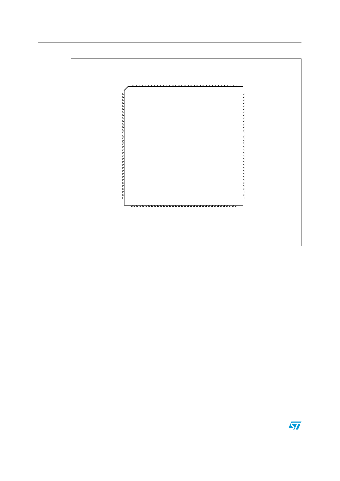
Figure 4. LQFP 144-pin configuration
PB[2]
PC[8]
PC[13]
PC[12]
PE[7]
PE[6]
PH[8]
PH[7]
PH[6]
PH[5]
PH[4]
PE[5]
PE[4]
PC[4]
PC[5]
PE[3]
PE[2]
PH[9]
PC[0]
VSS_LV
VDD_LV
VDD_HV
VSS_HV
PC[1]
PH[10]
PA[ 6 ]
PA[ 5 ]
PC[2]
PC[3]
PG[11]
PG[10]
PE[15]
PE[14]
PG[15]
PG[14]
PE[12]
144
143
142
141
140
139
138
137
136
135
134
133
132
131
130
129
128
127
126
125
124
123
122
121
120
119
118
117
116
115
114
113
112
111
110
PB[3]
PC[9]
PC[14]
PC[15]
PG[5]
PG[4]
PG[3]
PG[2]
PA[ 2 ]
PE[0]
PA[ 1 ]
PE[1]
PE[8]
PE[9]
PE[10]
PA[ 0 ]
PE[11]
VSS_HV
VDD_HV
VSS_HV
RESET
VSS_LV
VDD_LV
VDD_BV
PG[9]
PG[8]
PC[11]
PC[10]
PG[7]
PG[6]
PB[0]
PB[1]
PF[9]
PF[8]
PF[12]
PC[6]
1
2
3
4
5
6
7
8
9
10
11
12
13
14
15
16
17
18
19
20
21
22
23
24
25
26
27
28
29
30
31
32
33
34
35
36
LQFP144
To p v i ew
3738394041424344454647484950515253545556575859606162636465666768697071
109
108
107
106
105
104
103
102
101
100
72
99
98
97
96
95
94
93
92
91
90
89
88
87
86
85
84
83
82
81
80
79
78
77
76
75
74
73
PA[ 11 ]
PA[ 10 ]
PA[ 9]
PA[ 8]
PA[ 7]
PE[13]
PF[14]
PF[15]
VDD_HV
VSS_HV
PG[0]
PG[1]
PH[3]
PH[2]
PH[1]
PH[0]
PG[12]
PG[13]
PA[ 3]
PB[15]
PD[15]
PB[14]
PD[14]
PB[13]
PD[13]
PB[12]
PD[12]
PB[11]
PD[11]
PD[10]
PD[9]
PB[7]
PB[6]
PB[5]
VDD_HV_ADC
VSS_HV_ADC
PA[ 4 ]
PC[7]
PA[ 1 5]
PA[ 1 4]
PF[10]
PF[11]
PF[13]
XTAL
PA[ 1 3]
PA[ 1 2]
VSS_LV
VDD_LV
VSS_HV
PF[0]
PF[1]
PF[2]
PF[3]
PF[4]
PF[5]
PF[6]
PB[9]
PB[8]
PB[10]
EXTAL
VDD_HV
PF[7]
PD[0]
PD[1]
PD[2]
PD[3]
PB[4]
PD[4]
PD[5]
PD[6]
PD[7]
PD[8]
Note:
Availability of port pin alternate functions depends on product selection.
16/117 Doc ID 14619 Rev 9
SPC560B40x/50x, SPC560C40x/50x Package pinouts and signal descriptions
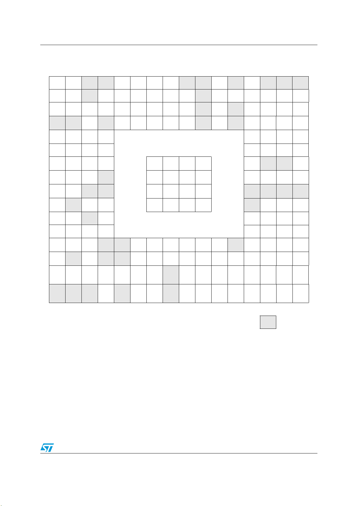
Figure 5. LBGA208 confguration
12345678910111213141516
A PC[8] PC[13]
BPC[9]PB[2]
CPC[14]
D
E PG[4] PG[5] PG[3] PG[2] PG[1] PG[0] PF[15]
F PE[0] PA[2] PA[1] PE[1] PH[0] PH[1] PH[3] PH[2] F
G PE[9] PE[8] PE[10] PA[0]
H
J RESET
K EVTI
L PG[9] PG[8]
M PG[7] PG[6] PC[10] PC[11] PB[13] PD[13] PD[12] PB[12] M
N PB[1] PF[9] PB[0]
PPF[8]
R PF[12] PC[6] PF[10] PF[11]
VDD_H
NC NC PC[15] NC PH[6] PE[4] PE[2]
VSS_H
PE[11]
V
VSS_L
NC NC PH[8] PH[4] PC[5] PC[0] NC NC PC[2] NC PE[15] NC NC NC A
NC PC[12] PE[6] PH[5] PC[4] PH[9] PH[10] NC PC[3] PG[11] PG[15] PG[14] PA[11] PA[10] B
VSS_L
PB[3] PE[7] PH[7] PE[5] PE[3]
V
VSS_HVVSS_HVVSS_HVVSS_H
VDD_H
V
VDD_BVVDD_L
NC
NC PC[7] NC NC PA[14]
NC
V
NC NC
V
NC EVTO PB[15] PD[15] PD[14] PB[14] L
NC NC PA[4]
VDD_H
V
VSS_HVVSS_HVVSS_HVVSS_H
VSS_HVVSS_HVVSS_HVVSS_H
VSS_HVVSS_HVVSS_HVVSS_H
VSS_L
V
VDD_L
V
PA [1 5 ] PA [ 13 ]
PC[1]
V
VDD_LVVDD_H
VDD_H
EXTAL
XTAL PB[10] PF[1] PF[5] PD[0] PD[3]
OSC32
NC
K_XTALPF[3] PF[7] PD[2] PD[4] PD[7]
NC PA[5] NC PE[14] PE[12] PA[9] PA[8] C
NC PA[6] NC PG[10] PF[14] PE[13] PA[7] D
V
V
V
V
V
PF[0] PF[4] NC PB[11] PD[10] PD[9] PD[11] N
V
VDD_H
MDO3 MDO2 MDO0 MDO1 H
NC NC NC NC J
NC PG[12] PA[3] PG[13] K
NC NC MSEO G
V
VDD_H
V_ADC
VSS_H
V_ADC
VDD_H
V
PB[6] PB[7] P
PB[5] R
E
NC NC NC MCKO NC PF[13] PA[12] NC
T
12345678910111213141516
Note: LBGA208 available only as development package for Nexus 2+.
OSC32
K_EXTALPF[2] PF[6] PD[1] PD[5] PD[6] PD[8] PB[4] T
= Not connected
NC
3.2 Pad configuration during reset phases
All pads have a fixed configuration under reset.
During the power-up phase, all pads are forced to tristate.
Doc ID 14619 Rev 9 17/117
Package pinouts and signal descriptions SPC560B40x/50x, SPC560C40x/50x
After power-up phase, all pads are forced to tristate with the following exceptions:
● PA[9] (FAB) is pull-down. Without external strong pull-up the device starts fetching from
flash.
● PA[8] (ABS[0]) is pull-up.
● RESET pad is driven low. This is pull-up only after PHASE2 reset completion.
● JTAG pads (TCK, TMS and TDI) are pull-up whilst TDO remains tristate.
● Precise ADC pads (PB[7:4] and PD[11:0]) are left tristate (no output buffer available).
● Main oscillator pads (EXTAL, XTAL) are tristate.
● Nexus output pads (MDO[n], MCKO, EVTO, MSEO) are forced to output.
3.3 Voltage supply pins
Voltage supply pins are used to provide power to the device. Three dedicated
VDD_LV/VSS_LV supply pairs are used for 1.2 V regulator stabilization.
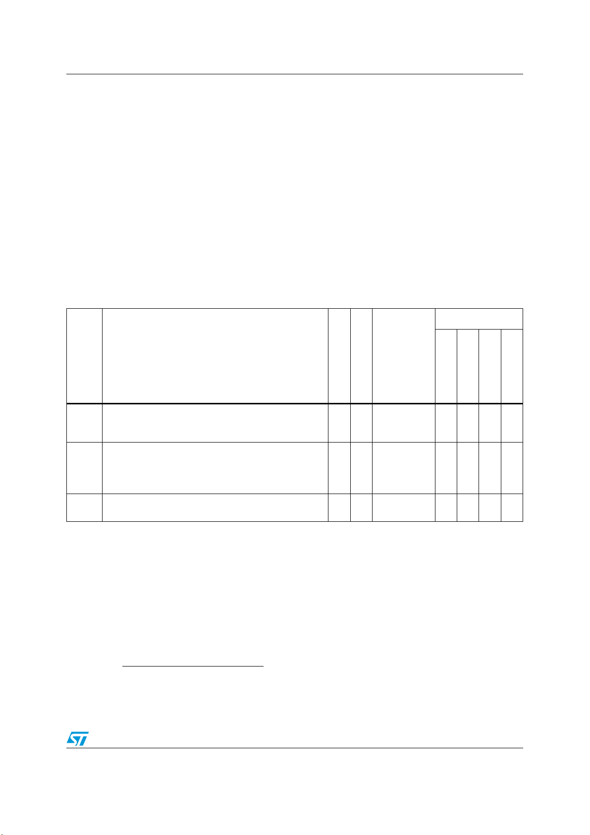
Table 4. Voltage supply pin descriptions
Port pin Function
Pin number
LQFP64 LQFP100 LQFP144 LBGA208
(1)
C2, D9, E16,
G13, H3,
N9, R5
VDD_HV Digital supply voltage 7, 28, 56
15, 37, 70, 8419, 51, 100,
123
G7, G8, G9,
G10, H1,
VSS_HV Digital ground 6, 8, 26, 55
14, 16, 35,
69, 83
18, 20, 49,
99, 122
H7, H8, H9,
H10, J7, J8,
J9, J10, K7,
K8, K9, K10
1.2V decoupling pins. Decoupling
VDD_LV
capacitor must be connected between
these pins and the nearest V
(2)
pin.
SS_LV
11, 23, 57 19, 32, 85 23, 46, 124 D8, K4, P7
1.2V decoupling pins. Decoupling
VSS_LV
capacitor must be connected between
these pins and the nearest V
(2)
pin.
DD_LV
10, 24, 58 18, 33, 86 22, 47, 125 C8, J2, N7
VDD_BV Internal regulator supply voltage 12 20 24 K3
VSS_HV_ADC
VDD_HV_ADC
1. LBGA208 available only as development package for Nexus2+.
2. A decoupling capacitor must be placed between each of the three VDD_LV/VSS_LV supply pairs to ensure stable voltage
(see the recommended operating conditions in the device datasheet for details).
Reference ground and analog ground
for the ADC
Reference voltage and analog supply
for the ADC
33 51 73 R15
34 52 74 P14
18/117 Doc ID 14619 Rev 9
SPC560B40x/50x, SPC560C40x/50x Package pinouts and signal descriptions
3.4 Pad types
In the device the following types of pads are available for system pins and functional port
pins:
S = Slow
M = Medium
F = Fast
I = Input only with analog feature
(b)
(b)(c)
(b)(c)
(b)
J = Input/Output (‘S’ pad) with analog feature
X = Oscillator
3.5 System pins
The system pins are listed in Ta bl e 5 .
Table 5. System pin descriptions
Pin number
Function
System pin
RESET
Bidirectional reset with Schmitt-Trigger characteristics
and noise filter.
Analog output of the oscillator amplifier circuit, when the
EXTAL
XTAL
1. LBGA208 available only as development package for Nexus2+.
2. See the relevant section of the datasheet .
oscillator is not in bypass mode.
Analog input for the clock generator when the oscillator
is in bypass mode.
(2)
Analog input of the oscillator amplifier circuit. Needs to
be grounded if oscillator is used in bypass mode.
(2)
Pad type
I/O direction
LQFP64
LQFP100
LQFP144
RESET configuration
Input, weak
I/O M
pull-up only
91721J1
after PHASE2
I/O X Tristate 27 36 50 N8
I X Tristate 25 34 48 P8
(1)
LBGA208
b. See the I/O pad electrical characteristics in the device datasheet for details.
c. All medium and fast pads are in slow configuration by default at reset and can be configured as fast or medium
(see PCR.SRC in section Pad Configuration Registers (PCR0–PCR122) in the device reference manual).
Doc ID 14619 Rev 9 19/117

20/117 Doc ID 14619 Rev 9
3.6 Functional ports
The functional port pins are listed in Ta bl e 6 .
Table 6. Functional port pin descriptions
(1)
Port pin
PA[0] PCR[0] AF0
PA[1] PCR[1] AF0
PA[2] PCR[2] AF0
PA[3] PCR[3] AF0
PA[4] PCR[4] AF0
PCR
Alternate
AF1
AF2
AF3
—
AF1
AF2
AF3
—
—
AF1
AF2
AF3
—
AF1
AF2
AF3
—
AF1
AF2
AF3
—
function
Function
GPIO[0]
E0UC[0]
CLKOUT
—
WKPU[19]
GPIO[1]
E0UC[1]
—
—
(5)
NMI
WKPU[2]
GPIO[2]
E0UC[2]
—
—
WKPU[3]
GPIO[3]
E0UC[3]
—
—
EIRQ[0]
GPIO[4]
E0UC[4]
—
—
WKPU[9]
(4)
(4)
(4)
(4)
Peripheral
SIUL
eMIOS_0
CGL
—
WKPU
SIUL
eMIOS_0
—
—
WKPU
WKPU
SIUL
eMIOS_0
—
—
WKPU
SIUL
eMIOS_0
—
—
SIUL
SIUL
eMIOS_0
—
—
WKPU
I/O
I/O
O
—
I/O
I/O
—
—
I/O
I/O
—
—
I/O
I/O
—
—
I/O
I/O
—
—
(2)
I/O direction
Pad type
RESET
configuration
LQFP64
Pin number
LQFP100
LQFP144
M Tristate 5 12 16 G4
I
S Tristate 4 7 11 F3
I
I
STristate 359F2
I
STristate 436890K15
I
S Tristate 20 29 43 N6
I
Package pinouts and signal descriptions SPC560B40x/50x, SPC560C40x/50x
(3)
LBGA208

Table 6. Functional port pin descriptions (continued)
(1)
Port pin
PA[5] PCR[5] AF0
PA[6] PCR[6] AF0
Doc ID 14619 Rev 9 21/117
PA[7] PCR[7] AF0
PA[8] PCR[8] AF0
PA[9] PCR[9] AF0
PA[10] PCR[10] AF0
PCR
Alternate
AF1
AF2
AF3
AF1
AF2
AF3
—
AF1
AF2
AF3
—
AF1
AF2
AF3
—
N/A
—
AF1
AF2
AF3
N/A
AF1
AF2
AF3
function
(6)
(6)
GPIO[5]
E0UC[5]
GPIO[6]
E0UC[6]
EIRQ[1]
GPIO[7]
E0UC[7]
LIN3TX
EIRQ[2]
GPIO[8]
E0UC[8]
EIRQ[3]
ABS[0]
LIN3RX
GPIO[9]
E0UC[9]
FAB
GPIO[10]
E0UC[10]
SDA
—
—
—
—
—
—
—
—
—
—
SPC560B40x/50x, SPC560C40x/50x Package pinouts and signal descriptions
(2)
Function
Peripheral
Pad type
I/O direction
SIUL
eMIOS_0
—
—
SIUL
eMIOS_0
—
—
SIUL
SIUL
eMIOS_0
LINFlex_3
—
SIUL
SIUL
eMIOS_0
—
—
SIUL
BAM
LINFlex_3
SIUL
eMIOS_0
—
—
BAM
SIUL
eMIOS_0
I2C_0
—
I/O
I/O
—
—
I/O
I/O
—
—
I/O
I/O
O
—
I/O
I/O
—
—
I/O
I/O
—
—
I/O
I/O
I/O
—
M Tristate 51 79 118 C11
S Tristate 52 80 119 D11
I
S Tristate 44 71 104 D16
I
S Input, weak
I
I
I
S Pull-down 46 73 106 C15
I
S Tristate 47 74 107 B16
RESET
pull-up
configuration
LQFP64
45 72 105 C16
Pin number
LQFP100
(3)
LQFP144
LBGA208

22/117 Doc ID 14619 Rev 9
Table 6. Functional port pin descriptions (continued)
(1)
Port pin
PA[11] PCR[11] AF0
PCR
Alternate
AF1
AF2
function
GPIO[11]
E0UC[11]
SCL
AF3
PA[12] PCR[12] AF0
GPIO[12]
AF1
AF2
AF3
—
PA[13] PCR[13] AF0
AF1
SIN_0
GPIO[13]
SOUT_0
AF2
AF3
PA[14] PCR[14] AF0
AF1
AF2
GPIO[14]
SCK_0
CS0_0
AF3
—
PA[15] PCR[15] AF0
AF1
AF2
EIRQ[4]
GPIO[15]
CS0_0
SCK_0
AF3
—
PB[0] PCR[16] AF0
AF1
WKPU[10]
GPIO[16]
CAN0TX
AF2
AF3
—
—
—
—
—
—
—
—
—
—
Package pinouts and signal descriptions SPC560B40x/50x, SPC560C40x/50x
(2)
Function
Peripheral
Pad type
I/O direction
(4)
SIUL
eMIOS_0
I2C_0
—
SIUL
—
—
—
DSPI0
SIUL
DSPI_0
—
—
SIUL
DSPI_0
DSPI_0
—
SIUL
SIUL
DSPI_0
DSPI_0
—
WKPU
SIUL
FlexCAN_0
—
—
I/O
I/O
I/O
—
I/O
—
—
—
I/O
O
—
—
I/O
I/O
I/O
—
I/O
I/O
I/O
—
I/O
O
—
—
S Tristate 48 75 108 B15
S Tristate 22 31 45 T7
I
M Tristate 21 30 44 R7
M Tristate 19 28 42 P6
I
M Tristate 18 27 40 R6
I
M Tristate 14 23 31 N3
RESET
configuration
LQFP64
Pin number
LQFP100
(3)
LQFP144
LBGA208

Table 6. Functional port pin descriptions (continued)
(1)
Port pin
PB[1] PCR[17] AF0
PB[2] PCR[18] AF0
Doc ID 14619 Rev 9 23/117
PB[3] PCR[19] AF0
PB[4] PCR[20] AF0
PB[5] PCR[21] AF0
PB[6] PCR[22] AF0
PCR
Alternate
AF1
AF2
AF3
—
—
AF1
AF2
AF3
AF1
AF2
AF3
—
—
AF1
AF2
AF3
—
AF1
AF2
AF3
—
AF1
AF2
AF3
—
function
GPIO[17]
WKPU[4]
CAN0RX
GPIO[18]
LIN0TX
SDA
GPIO[19]
SCL
WKPU[11]
LIN0RX
GPIO[20]
GPI[0]
GPIO[21]
GPI[1]
GPIO[22]
GPI[2]
—
—
—
—
—
—
—
—
—
—
—
—
—
—
—
SPC560B40x/50x, SPC560C40x/50x Package pinouts and signal descriptions
(2)
Function
Peripheral
Pad type
I/O direction
(4)
(4)
SIUL
—
—
—
WKPU
FlexCAN_0
SIUL
LINFlex_0
I2C_0
—
SIUL
—
I2C_0
—
WKPU
LINFlex_0
SIUL
—
—
—
ADC
SIUL
—
—
—
ADC
SIUL
—
—
—
ADC
I/O
—
—
—
I/O
O
I/O
—
I/O
—
I/O
—
—
—
—
—
—
—
—
—
—
S Tristate 15 24 32 N1
I
I
M Tristate 64 100 144 B2
STristate 111C3
I
I
I
ITristate 325072T16
I
I
I Tristate 35 53 75 R16
I
I
ITristate 365476P15
I
RESET
configuration
LQFP64
Pin number
LQFP100
(3)
LQFP144
LBGA208

24/117 Doc ID 14619 Rev 9
Table 6. Functional port pin descriptions (continued)
(1)
Port pin
PB[7] PCR[23] AF0
PCR
Alternate
function
GPIO[23]
AF1
AF2
AF3
—
PB[8] PCR[24] AF0
GPI[3]
GPIO[24]
AF1
AF2
AF3
—
—
PB[9] PCR[25] AF0
ANS[0]
OSC32K_XTAL
GPIO[25]
AF1
AF2
AF3
—
—
PB[10] PCR[26] AF0
ANS[1]
OSC32K_EXTAL
GPIO[26]
AF1
AF2
AF3
PB[11]
(8)
PCR[27] AF0
—
—
AF1
ANS[2]
WKPU[8]
GPIO[27]
E0UC[3]
AF2
AF3
—
CS0_0
ANS[3]
—
—
—
—
—
—
—
—
—
—
—
—
—
Package pinouts and signal descriptions SPC560B40x/50x, SPC560C40x/50x
(2)
Function
Peripheral
Pad type
I/O direction
(4)
(7)
(7)
SIUL
—
—
—
ADC
SIUL
—
—
—
ADC
SXOSC
SIUL
—
—
—
ADC
SXOSC
SIUL
—
—
—
ADC
WKPU
SIUL
eMIOS_0
—
DSPI_0
ADC
—
—
—
—
—
—
I/O
—
—
—
I/O
I/O
—
—
—
I/O
I/O
—
I/O
I
ITristate 375577P16
I
I
I Tristate 30 39 53 R9
I
I
I Tristate 29 38 52 T9
I
J Tristate 31 40 54 P9
I
I
J Tristate 38 59 81 N13
I
RESET
configuration
LQFP64
Pin number
LQFP100
(3)
LQFP144
LBGA208

Table 6. Functional port pin descriptions (continued)
(1)
PCR
Alternate
AF1
AF2
AF3
—
AF1
AF2
AF3
—
AF1
AF2
AF3
—
AF1
AF2
AF3
—
PCR[32] AF0
AF1
AF2
AF3
PCR[33] AF0
AF1
AF2
AF3
function
GPIO[28]
E0UC[4]
CS1_0
ANX[0]
GPIO[29]
E0UC[5]
CS2_0
ANX[1]
GPIO[30]
E0UC[6]
CS3_0
ANX[2]
GPIO[31]
E0UC[7]
CS4_0
ANX[3]
GPIO[32]
GPIO[33]
TDO
Doc ID 14619 Rev 9 25/117
Port pin
PB[12] PCR[28] AF0
PB[13] PCR[29] AF0
PB[14] PCR[30] AF0
PB[15] PCR[31] AF0
(9)
PC[0]
(9)
PC[1]
—
—
—
—
—
TDI
—
—
—
Function
(10)
Peripheral
SIUL
eMIOS_0
—
DSPI_0
ADC
SIUL
eMIOS_0
—
DSPI_0
ADC
SIUL
eMIOS_0
—
DSPI_0
ADC
SIUL
eMIOS_0
—
DSPI_0
ADC
SIUL
—
JTAGC
—
SIUL
—
JTAGC
—
I/O
I/O
—
O
I/O
I/O
—
O
I/O
I/O
—
O
I/O
I/O
—
O
I/O
—
—
I/O
—
O
—
(2)
Pad type
I/O direction
RESET
configuration
LQFP64
Pin number
LQFP100
LQFP144
JTristate 396183M16
I
JTristate 406385M13
I
J Tristate 41 65 87 L16
I
J Tristate 42 67 89 L13
I
M Input, weak
59 87 126 A8
pull-up
I
MTristate 54 82121C9
SPC560B40x/50x, SPC560C40x/50x Package pinouts and signal descriptions
(3)
LBGA208

26/117 Doc ID 14619 Rev 9
Table 6. Functional port pin descriptions (continued)
(1)
Port pin
PC[2] PCR[34] AF0
PCR
Alternate
AF1
AF2
function
GPIO[34]
SCK_1
CAN4TX
AF3
—
PC[3] PCR[35] AF0
AF1
AF2
EIRQ[5]
GPIO[35]
CS0_1
MA[0]
AF3
—
—
—
PC[4] PCR[36] AF0
CAN1RX
CAN4RX
EIRQ[6]
GPIO[36]
AF1
AF2
AF3
—
—
PC[5] PCR[37] AF0
AF1
AF2
SIN_1
CAN3RX
GPIO[37]
SOUT_1
CAN3TX
AF3
—
PC[6] PCR[38] AF0
AF1
EIRQ[7]
GPIO[38]
LIN1TX
AF2
AF3
—
—
—
—
—
—
—
—
Package pinouts and signal descriptions SPC560B40x/50x, SPC560C40x/50x
(2)
Function
Peripheral
Pad type
I/O direction
(11)
(11)
(11)
(11)
SIUL
DSPI_1
FlexCAN_4
—
SIUL
SIUL
DSPI_1
ADC
—
FlexCAN_1
FlexCAN_4
SIUL
SIUL
—
—
—
DSPI_1
FlexCAN_3
SIUL
DSPI1
FlexCAN_3
—
SIUL
SIUL
LINFlex_1
—
—
I/O
I/O
O
—
I/O
I/O
O
—
I/O
—
—
—
I/O
O
O
—
I/O
O
—
—
M Tristate 50 78 117 A11
I
S Tristate 49 77 116 B11
I
I
I
MTristate 62 92131B7
I
I
MTristate 61 91130A7
I
S Tristate 16 25 36 R2
RESET
configuration
LQFP64
Pin number
LQFP100
(3)
LQFP144
LBGA208

Table 6. Functional port pin descriptions (continued)
(1)
Port pin
PC[7] PCR[39] AF0
PC[8] PCR[40] AF0
Doc ID 14619 Rev 9 27/117
PC[9] PCR[41] AF0
PC[10] PCR[42] AF0
PC[11] PCR[43] AF0
PCR
Alternate
AF1
AF2
AF3
—
—
AF1
AF2
AF3
AF1
AF2
AF3
—
—
AF1
AF2
AF3
AF1
AF2
AF3
—
—
—
function
GPIO[39]
LIN1RX
WKPU[12]
GPIO[40]
LIN2TX
GPIO[41]
LIN2RX
WKPU[13]
GPIO[42]
CAN1TX
CAN4TX
MA[1]
GPIO[43]
CAN1RX
CAN4RX
WKPU[5]
—
—
—
—
—
—
—
—
—
—
—
SPC560B40x/50x, SPC560C40x/50x Package pinouts and signal descriptions
(2)
Function
Peripheral
Pad type
I/O direction
(11)
(11)
(4)
(4)
(4)
SIUL
—
—
—
LINFlex_1
WKPU
SIUL
LINFlex_2
—
—
SIUL
—
—
—
LINFlex_2
WKPU
SIUL
FlexCAN_1
FlexCAN_4
ADC
SIUL
—
—
—
FlexCAN_1
FlexCAN_4
WKPU
I/O
—
—
—
I/O
O
—
—
I/O
—
—
—
I/O
O
O
O
I/O
—
—
—
S Tristate 17 26 37 P3
I
I
STristate 6399143A1
STristate 222B1
I
I
M Tristate 13 22 28 M3
S Tristate — 21 27 M4
I
I
I
RESET
configuration
LQFP64
Pin number
LQFP100
(3)
LQFP144
LBGA208

28/117 Doc ID 14619 Rev 9
Table 6. Functional port pin descriptions (continued)
(1)
Port pin
PC[12] PCR[44] AF0
PCR
Alternate
AF1
function
GPIO[44]
E0UC[12]
AF2
AF3
—
PC[13] PCR[45] AF0
AF1
AF2
SIN_2
GPIO[45]
E0UC[13]
SOUT_2
AF3
PC[14] PCR[46] AF0
AF1
AF2
GPIO[46]
E0UC[14]
SCK_2
AF3
—
PC[15] PCR[47] AF0
AF1
AF2
EIRQ[8]
GPIO[47]
E0UC[15]
CS0_2
AF3
PD[0] PCR[48] AF0
GPIO[48]
AF1
AF2
AF3
—
PD[1] PCR[49] AF0
GPI[4]
GPIO[49]
AF1
AF2
AF3
—
GPI[5]
—
—
—
—
—
—
—
—
—
—
—
Package pinouts and signal descriptions SPC560B40x/50x, SPC560C40x/50x
(2)
Function
Peripheral
Pad type
I/O direction
SIUL
eMIOS_0
—
—
DSPI_2
SIUL
eMIOS_0
DSPI_2
—
SIUL
eMIOS_0
DSPI_2
—
SIUL
SIUL
eMIOS_0
DSPI_2
—
SIUL
—
—
—
ADC
SIUL
—
—
—
ADC
I/O
I/O
—
—
I/O
I/O
O
—
I/O
I/O
I/O
—
I/O
I/O
I/O
—
—
—
—
—
—
—
M Tristate — 97 141 B4
I
S Tristate — 98 142 A2
STristate — 3 3 C1
I
MTristate — 4 4 D3
I
I Tristate — 41 63 P12
I
I
I Tristate — 42 64 T12
I
RESET
configuration
LQFP64
Pin number
LQFP100
(3)
LQFP144
LBGA208

Table 6. Functional port pin descriptions (continued)
(1)
Port pin
PD[2] PCR[50] AF0
PD[3] PCR[51] AF0
Doc ID 14619 Rev 9 29/117
PD[4] PCR[52] AF0
PD[5] PCR[53] AF0
PD[6] PCR[54] AF0
PD[7] PCR[55] AF0
PCR
Alternate
AF1
AF2
AF3
—
AF1
AF2
AF3
—
AF1
AF2
AF3
—
AF1
AF2
AF3
—
AF1
AF2
AF3
—
AF1
AF2
AF3
—
function
GPIO[50]
GPI[6]
GPIO[51]
GPI[7]
GPIO[52]
GPI[8]
GPIO[53]
GPI[9]
GPIO[54]
GPI[10]
GPIO[55]
GPI[11]
—
—
—
—
—
—
—
—
—
—
—
—
—
—
—
—
—
—
SPC560B40x/50x, SPC560C40x/50x Package pinouts and signal descriptions
(2)
Function
Peripheral
Pad type
I/O direction
SIUL
—
—
—
ADC
SIUL
—
—
—
ADC
SIUL
—
—
—
ADC
SIUL
—
—
—
ADC
SIUL
—
—
—
ADC
SIUL
—
—
—
ADC
—
—
—
—
—
—
—
—
—
—
—
—
—
—
—
—
—
—
I
I Tristate — 43 65 R12
I
I
I Tristate — 44 66 P13
I
I
I Tristate — 45 67 R13
I
I
I Tristate — 46 68 T13
I
I Tristate — 47 69 T14
I
I
I
I Tristate — 48 70 R14
I
RESET
configuration
LQFP64
Pin number
LQFP100
(3)
LQFP144
LBGA208

30/117 Doc ID 14619 Rev 9
Table 6. Functional port pin descriptions (continued)
(1)
Port pin
PD[8] PCR[56] AF0
PCR
Alternate
function
GPIO[56]
AF1
AF2
AF3
—
PD[9] PCR[57] AF0
GPI[12]
GPIO[57]
AF1
AF2
AF3
—
PD[10] PCR[58] AF0
GPI[13]
GPIO[58]
AF1
AF2
AF3
—
PD[11] PCR[59] AF0
GPI[14]
GPIO[59]
AF1
AF2
AF3
PD[12]
(8)
PCR[60] AF0
—
AF1
AF2
GPI[15]
GPIO[60]
CS5_0
E0UC[24]
AF3
—
PD[13] PCR[61] AF0
AF1
AF2
ANS[4]
GPIO[61]
CS0_1
E0UC[25]
AF3
—
ANS[5]
—
—
—
—
—
—
—
—
—
—
—
—
—
—
Package pinouts and signal descriptions SPC560B40x/50x, SPC560C40x/50x
(2)
Function
Peripheral
Pad type
I/O direction
SIUL
—
—
—
ADC
SIUL
—
—
—
ADC
SIUL
—
—
—
ADC
SIUL
—
—
—
ADC
SIUL
DSPI_0
eMIOS_0
—
ADC
SIUL
DSPI_1
eMIOS_0
—
ADC
—
—
—
—
—
—
—
—
—
—
—
—
I/O
O
I/O
—
I/O
I/O
I/O
—
I
I Tristate — 49 71 T15
I
I
I Tristate — 56 78 N15
I
I
I Tristate — 57 79 N14
I
I
I Tristate — 58 80 N16
I
J Tristate — 60 82 M15
I
J Tristate — 62 84 M14
I
RESET
configuration
LQFP64
Pin number
LQFP100
(3)
LQFP144
LBGA208

Table 6. Functional port pin descriptions (continued)
(1)
Port pin
PD[14] PCR[62] AF0
PD[15] PCR[63] AF0
Doc ID 14619 Rev 9 31/117
PE[0] PCR[64] AF0
PE[1] PCR[65] AF0
PE[2] PCR[66] AF0
PE[3] PCR[67] AF0
PCR
Alternate
AF1
AF2
AF3
—
AF1
AF2
AF3
—
AF1
AF2
AF3
—
—
AF1
AF2
AF3
AF1
AF2
AF3
—
AF1
AF2
AF3
function
GPIO[62]
CS1_1
E0UC[26]
ANS[6]
GPIO[63]
CS2_1
E0UC[27]
ANS[7]
GPIO[64]
E0UC[16]
CAN5RX
WKPU[6]
GPIO[65]
E0UC[17]
CAN5TX
GPIO[66]
E0UC[18]
SIN_1
GPIO[67]
E0UC[19]
SOUT_1
—
—
—
—
—
—
—
—
SPC560B40x/50x, SPC560C40x/50x Package pinouts and signal descriptions
(2)
Function
Peripheral
Pad type
I/O direction
(11)
(4)
(11)
SIUL
DSPI_1
eMIOS_0
—
ADC
SIUL
DSPI_1
eMIOS_0
—
ADC
SIUL
eMIOS_0
—
—
FlexCAN_5
WKPU
SIUL
eMIOS_0
FlexCAN_5
—
SIUL
eMIOS_0
—
—
DSPI_1
SIUL
eMIOS_0
DSPI_1
—
I/O
O
I/O
—
I/O
O
I/O
—
I/O
I/O
—
—
I/O
I/O
O
—
I/O
I/O
—
—
I/O
I/O
O
—
J Tristate — 64 86 L15
I
J Tristate — 66 88 L14
I
S Tristate — 6 10 F1
I
I
M Tristate — 8 12 F4
M Tristate — 89 128 D7
I
M Tristate — 90 129 C7
RESET
configuration
LQFP64
Pin number
LQFP100
(3)
LQFP144
LBGA208

32/117 Doc ID 14619 Rev 9
Table 6. Functional port pin descriptions (continued)
(1)
Port pin
PE[4] PCR[68] AF0
PCR
Alternate
AF1
AF2
function
GPIO[68]
E0UC[20]
SCK_1
AF3
—
PE[5] PCR[69] AF0
AF1
AF2
AF3
PE[6] PCR[70] AF0
AF1
AF2
AF3
PE[7] PCR[71] AF0
AF1
AF2
AF3
PE[8] PCR[72] AF0
AF1
AF2
AF3
PE[9] PCR[73] AF0
EIRQ[9]
GPIO[69]
E0UC[21]
CS0_1
MA[2]
GPIO[70]
E0UC[22]
CS3_0
MA[1]
GPIO[71]
E0UC[23]
CS2_0
MA[0]
GPIO[72]
CAN2TX
E0UC[22]
CAN3TX
GPIO[73]
AF1
AF2
E0UC[23]
AF3
—
—
—
WKPU[7]
CAN2RX
CAN3RX
—
—
—
Package pinouts and signal descriptions SPC560B40x/50x, SPC560C40x/50x
(2)
Function
Peripheral
Pad type
I/O direction
(12)
(11)
(4)
(12)
(11)
SIUL
eMIOS_0
DSPI_1
—
SIUL
SIUL
eMIOS_0
DSPI_1
ADC
SIUL
eMIOS_0
DSPI_0
ADC
SIUL
eMIOS_0
DSPI_0
ADC
SIUL
FlexCAN_2
eMIOS_0
FlexCAN_3
SIUL
—
eMIOS_0
—
WKPU
FlexCAN_2
FlexCAN_3
I/O
I/O
I/O
—
I/O
I/O
I/O
O
I/O
I/O
O
O
I/O
I/O
O
O
I/O
O
I/O
O
I/O
—
I/O
—
M Tristate — 93 132 D6
I
M Tristate — 94 133 C6
M Tristate — 95 139 B5
M Tristate — 96 140 C4
M Tristate — 9 13 G2
S Tristate — 10 14 G1
I
I
I
RESET
configuration
LQFP64
Pin number
LQFP100
(3)
LQFP144
LBGA208

Table 6. Functional port pin descriptions (continued)
(1)
Port pin
PE[10] PCR[74] AF0
PE[11] PCR[75] AF0
Doc ID 14619 Rev 9 33/117
PE[12] PCR[76] AF0
PE[13] PCR[77] AF0
PE[14] PCR[78] AF0
PE[15] PCR[79] AF0
PCR
Alternate
AF1
AF2
AF3
—
AF1
AF2
AF3
—
—
AF1
AF2
AF3
—
—
AF1
AF2
AF3
AF1
AF2
AF3
—
AF1
AF2
AF3
function
GPIO[74]
LIN3TX
CS3_1
EIRQ[10]
GPIO[75]
CS4_1
LIN3RX
WKPU[14]
GPIO[76]
E1UC[19]
SIN_2
EIRQ[11]
GPIO[77]
SOUT2
E1UC[20]
GPIO[78]
SCK_2
E1UC[21]
EIRQ[12]
GPIO[79]
CS0_2
E1UC[22]
—
—
—
—
—
—
—
—
SPC560B40x/50x, SPC560C40x/50x Package pinouts and signal descriptions
(2)
Function
Peripheral
Pad type
I/O direction
(4)
(13)
SIUL
LINFlex_3
DSPI_1
—
SIUL
SIUL
—
DSPI_1
—
LINFlex_3
WKPU
SIUL
—
eMIOS_1
—
DSPI_2
SIUL
SIUL
DSPI_2
eMIOS_1
—
SIUL
DSPI_2
eMIOS_1
—
SIUL
SIUL
DSPI_2
eMIOS_1
—
I/O
O
O
—
I/O
—
O
—
I/O
—
I/O
—
I/O
O
I/O
—
I/O
I/O
I/O
—
I/O
I/O
I/O
—
S Tristate — 11 15 G3
I
S Tristate — 13 17 H2
I
I
S Tristate — 76 109 C14
I
I
S Tristate — — 103 D15
S Tristate — — 112 C13
I
M Tristate — — 113 A13
RESET
configuration
LQFP64
Pin number
LQFP100
(3)
LQFP144
LBGA208

34/117 Doc ID 14619 Rev 9
Table 6. Functional port pin descriptions (continued)
(1)
Port pin
PF[0] PCR[80] AF0
PCR
Alternate
AF1
AF2
function
GPIO[80]
E0UC[10]
CS3_1
AF3
—
PF[1] PCR[81] AF0
AF1
AF2
ANS[8]
GPIO[81]
E0UC[11]
CS4_1
AF3
—
PF[2] PCR[82] AF0
AF1
AF2
ANS[9]
GPIO[82]
E0UC[12]
CS0_2
AF3
—
PF[3] PCR[83] AF0
AF1
AF2
ANS[10]
GPIO[83]
E0UC[13]
CS1_2
AF3
—
PF[4] PCR[84] AF0
AF1
AF2
ANS[11]
GPIO[84]
E0UC[14]
CS2_2
AF3
—
PF[5] PCR[85] AF0
AF1
AF2
ANS[12]
GPIO[85]
E0UC[22]
CS3_2
AF3
—
ANS[13]
—
—
—
—
—
—
Package pinouts and signal descriptions SPC560B40x/50x, SPC560C40x/50x
(2)
Function
Peripheral
Pad type
I/O direction
SIUL
eMIOS_0
DSPI_1
—
ADC
SIUL
eMIOS_0
DSPI_1
—
I
SIUL
eMIOS_0
DSPI_2
—
ADC
SIUL
eMIOS_0
DSPI_2
—
ADC
SIUL
eMIOS_0
DSPI_2
—
ADC
SIUL
eMIOS_0
DSPI_2
—
ADC
I/O
I/O
O
—
I/O
I/O
O
—
I/O
I/O
I/O
—
I/O
I/O
O
—
I/O
I/O
O
—
I/O
I/O
O
—
J Tristate — — 55 N10
I
JTristate ——56P10
I
JTristate ——57T10
I
J Tristate — — 58 R10
I
J Tristate — — 59 N11
I
JTristate ——60P11
I
RESET
configuration
LQFP64
Pin number
LQFP100
(3)
LQFP144
LBGA208

Table 6. Functional port pin descriptions (continued)
(1)
Port pin
PF[6] PCR[86] AF0
PF[7] PCR[87] AF0
Doc ID 14619 Rev 9 35/117
PF[8] PCR[88] AF0
PF[9] PCR[89] AF0
PF[10] PCR[90] AF0
PF[11] PCR[91] AF0
PCR
Alternate
AF1
AF2
AF3
—
AF1
AF2
AF3
—
AF1
AF2
AF3
AF1
AF2
AF3
—
—
AF1
AF2
AF3
AF1
AF2
AF3
—
function
GPIO[86]
E0UC[23]
ANS[14]
GPIO[87]
ANS[15]
GPIO[88]
CAN3TX
CS4_0
CAN2TX
GPIO[89]
CS5_0
CAN2RX
CAN3RX
GPIO[90]
GPIO[91]
WKPU[15]
—
—
—
—
—
—
—
—
—
—
—
—
—
SPC560B40x/50x, SPC560C40x/50x Package pinouts and signal descriptions
(2)
Function
Peripheral
Pad type
I/O direction
(14)
(15)
(15)
(14)
(4)
SIUL
eMIOS_0
—
—
ADC
SIUL
—
—
—
ADC
SIUL
FlexCAN_3
DSPI_0
FlexCAN_2
SIUL
—
DSPI_0
—
FlexCAN_2
FlexCAN_3
SIUL
—
—
—
SIUL
—
—
—
WKPU
I/O
I/O
—
—
I/O
—
—
—
I/O
O
O
O
I/O
—
O
—
I/O
—
—
—
I/O
—
—
—
JTristate ——61T11
I
J Tristate — — 62 R11
I
M Tristate — — 34 P1
S Tristate — — 33 N2
I
I
M Tristate — — 38 R3
S Tristate — — 39 R4
I
RESET
configuration
LQFP64
Pin number
LQFP100
(3)
LQFP144
LBGA208

36/117 Doc ID 14619 Rev 9
Table 6. Functional port pin descriptions (continued)
(1)
Port pin
PF[12] PCR[92] AF0
PCR
Alternate
AF1
function
GPIO[92]
E1UC[25]
AF2
AF3
PF[13] PCR[93] AF0
AF1
GPIO[93]
E1UC[26]
AF2
AF3
—
PF[14] PCR[94] AF0
AF1
AF2
AF3
PF[15] PCR[95] AF0
WKPU[16]
GPIO[94]
CAN4TX
E1UC[27]
CAN1TX
GPIO[95]
AF1
AF2
AF3
—
—
—
PG[0] PCR[96] AF0
AF1
AF2
CAN1RX
CAN4RX
EIRQ[13]
GPIO[96]
CAN5TX
E1UC[23]
AF3
PG[1] PCR[97] AF0
GPIO[97]
AF1
AF2
E1UC[24]
AF3
—
—
CAN5RX
EIRQ[14]
—
—
—
—
—
—
—
—
—
—
Package pinouts and signal descriptions SPC560B40x/50x, SPC560C40x/50x
(2)
Function
Peripheral
Pad type
I/O direction
(11)
(11)
(11)
(11)
(4)
SIUL
eMIOS_1
—
—
SIUL
eMIOS_1
—
—
WKPU
SIUL
FlexCAN_4
eMIOS_1
FlexCAN_4
SIUL
—
—
—
FlexCAN_1
FlexCAN_4
SIUL
SIUL
FlexCAN_5
eMIOS_1
—
SIUL
—
eMIOS_1
—
FlexCAN_5
SIUL
I/O
I/O
—
—
I/O
I/O
—
—
I/O
O
I/O
O
I/O
—
—
—
I/O
O
I/O
—
I/O
—
I/O
—
M Tristate — — 35 R1
S Tristate — — 41 T6
I
M Tristate — — 102 D14
S Tristate — — 101 E15
I
I
I
MTristate — — 98E14
STristate — — 97E13
I
I
RESET
configuration
LQFP64
Pin number
LQFP100
(3)
LQFP144
LBGA208

Table 6. Functional port pin descriptions (continued)
(1)
Port pin
PG[2] PCR[98] AF0
PG[3] PCR[99] AF0
Doc ID 14619 Rev 9 37/117
PG[4] PCR[100] AF0
PG[5] PCR[101] AF0
PG[6] PCR[102] AF0
PG[7] PCR[103] AF0
PCR
Alternate
AF1
AF2
AF3
AF1
AF2
AF3
—
AF1
AF2
AF3
AF1
AF2
AF3
—
AF1
AF2
AF3
AF1
AF2
AF3
function
GPIO[98]
E1UC[11]
GPIO[99]
E1UC[12]
WKPU[17]
GPIO[100]
E1UC[13]
GPIO[101]
E1UC[14]
WKPU[18]
GPIO[102]
E1UC[15]
GPIO[103]
E1UC[16]
—
—
—
—
—
—
—
—
—
—
—
—
SPC560B40x/50x, SPC560C40x/50x Package pinouts and signal descriptions
(2)
Function
Peripheral
Pad type
I/O direction
(4)
(4)
SIUL
eMIOS_1
—
—
SIUL
eMIOS_1
—
—
WKPU
SIUL
eMIOS_1
—
—
SIUL
eMIOS_1
—
—
WKPU
SIUL
eMIOS_1
—
—
SIUL
eMIOS_1
—
—
I/O
I/O
—
—
I/O
I/O
—
—
I/O
I/O
—
—
I/O
I/O
—
—
I/O
I/O
—
—
I/O
I/O
—
—
MTristate — — 8 E4
STristate — — 7 E3
I
MTristate — — 6 E1
STristate — — 5 E2
I
M Tristate — — 30 M2
M Tristate — — 29 M1
RESET
configuration
LQFP64
Pin number
LQFP100
(3)
LQFP144
LBGA208

38/117 Doc ID 14619 Rev 9
Table 6. Functional port pin descriptions (continued)
(1)
Port pin
PG[8] PCR[104] AF0
PCR
Alternate
AF1
function
GPIO[104]
E1UC[17]
AF2
AF3
—
PG[9] PCR[105] AF0
AF1
CS0_2
EIRQ[15]
GPIO[105]
E1UC[18]
AF2
AF3
PG[10] PCR[106] AF0
AF1
SCK_2
GPIO[106]
E0UC[24]
AF2
AF3
PG[11] PCR[107] AF0
AF1
GPIO[107]
E0UC[25]
AF2
AF3
PG[12] PCR[108] AF0
AF1
GPIO[108]
E0UC[26]
AF2
AF3
PG[13] PCR[109] AF0
AF1
GPIO[109]
E0UC[27]
AF2
AF3
PG[14] PCR[110] AF0
AF1
GPIO[110]
E1UC[0]
AF2
AF3
—
—
—
—
—
—
—
—
—
—
—
—
Package pinouts and signal descriptions SPC560B40x/50x, SPC560C40x/50x
(2)
Function
Peripheral
Pad type
I/O direction
SIUL
eMIOS_1
—
DSPI_2
SIUL
SIUL
eMIOS_1
—
DSPI_2
SIUL
eMIOS_0
—
—
SIUL
eMIOS_0
—
—
SIUL
eMIOS_0
—
—
SIUL
eMIOS_0
—
—
SIUL
eMIOS_1
—
—
I/O
I/O
—
I/O
I/O
I/O
—
I/O
I/O
I/O
—
—
I/O
I/O
—
—
I/O
I/O
—
—
I/O
I/O
—
—
I/O
I/O
—
—
S Tristate — — 26 L2
I
S Tristate — — 25 L1
S Tristate — — 114 D13
M Tristate — — 115 B12
MTristate — — 92K14
MTristate — — 91K16
S Tristate — — 110 B14
RESET
configuration
LQFP64
Pin number
LQFP100
(3)
LQFP144
LBGA208

Table 6. Functional port pin descriptions (continued)
(1)
Port pin
PG[15] PCR[111] AF0
PH[0] PCR[112] AF0
Doc ID 14619 Rev 9 39/117
PH[1] PCR[113] AF0
PH[2] PCR[114] AF0
PH[3] PCR[115] AF0
PH[4] PCR[116] AF0
PH[5] PCR[117] AF0
PCR
Alternate
AF1
AF2
AF3
AF1
AF2
AF3
—
AF1
AF2
AF3
AF1
AF2
AF3
AF1
AF2
AF3
AF1
AF2
AF3
AF1
AF2
AF3
function
GPIO[111]
E1UC[1]
GPIO[112]
E1UC[2]
SIN1
GPIO[113]
E1UC[3]
SOUT1
GPIO[114]
E1UC[4]
SCK_1
GPIO[115]
E1UC[5]
CS0_1
GPIO[116]
E1UC[6]
GPIO[117]
E1UC[7]
—
—
—
—
—
—
—
—
—
—
—
SPC560B40x/50x, SPC560C40x/50x Package pinouts and signal descriptions
(2)
Function
Peripheral
Pad type
I/O direction
SIUL
eMIOS_1
—
—
SIUL
eMIOS_1
—
—
DSPI_1
SIUL
eMIOS_1
DSPI_1
—
SIUL
eMIOS_1
DSPI_1
—
SIUL
eMIOS_1
DSPI_1
—
SIUL
eMIOS_1
—
—
SIUL
eMIOS_1
—
—
I/O
I/O
—
—
I/O
I/O
—
—
I/O
I/O
O
—
I/O
I/O
I/O
—
I/O
I/O
I/O
—
I/O
I/O
—
—
I/O
I/O
—
—
M Tristate — — 111 B13
MTristate — — 93F13
I
MTristate — — 94F14
MTristate — — 95F16
MTristate — — 96F15
MTristate — —134A6
STristate — —135B6
RESET
configuration
LQFP64
Pin number
LQFP100
(3)
LQFP144
LBGA208

40/117 Doc ID 14619 Rev 9
Table 6. Functional port pin descriptions (continued)
Pin number
LQFP100
I/O
I/O
—
O
I/O
I/O
O
O
I/O
I/O
O
O
I/O
—
—
I/O
—
—
(2)
Pad type
I/O direction
RESET
configuration
LQFP64
MTristate — —136D5
MTristate — —137C5
MTristate — —138A5
S Input, weak
60 88 127 B8
pull-up
I
S Input, weak
60 81 120 B9
pull-up
I
(1)
Port pin
PH[6] PCR[118] AF0
PH[7] PCR[119] AF0
PH[8] PCR[120] AF0
(9)
PH[9]
(9)
PH[10]
1. Alternate functions are chosen by setting the values of the PCR.PA bitfields inside the SIUL module. PCR.PA = 00 → AF0; PCR.PA = 01 → AF1; PCR.PA = 10 → AF2;
PCR.PA = 11 → AF3. This is intended to select the output functions; to use one of the input functions, the PCR.IBE bit must be written to ‘1’, regardless of the values
selected in the PCR.PA bitfields. For this reason, the value corresponding to an input only function is reported as “—”.
2. Multiple inputs are routed to all respective modules internally. The input of some modules must be configured by setting the values of the PSMIO.PADSELx bitfields inside
the SIUL module.
3. LBGA208 available only as development package for Nexus2+.
4. All WKPU pins also support external interrupt capability. See wakeup unit chapter for further details.
5. NMI has higher priority than alternate function. When NMI is selected, the PCR.AF field is ignored.
6. “Not applicable” because these functions are available only while the device is booting. Refer to BAM chapter of the reference manual for details.
7. Value of PCR.IBE bit must be 0.
PCR
Alternate
AF1
AF2
AF3
AF1
AF2
AF3
AF1
AF2
AF3
PCR[121] AF0
AF1
AF2
AF3
PCR[122] AF0
AF1
AF2
AF3
function
Function
GPIO[118]
E1UC[8]
—
MA[2]
GPIO[119]
E1UC[9]
CS3_2
MA[1]
GPIO[120]
E1UC[10]
CS2_2
MA[0]
GPIO[121]
—
TCK
—
GPIO[122]
—
TMS
—
Peripheral
SIUL
eMIOS_1
—
ADC
SIUL
eMIOS_1
DSPI_2
ADC
SIUL
eMIOS_1
DSPI_2
ADC
SIUL
—
JTAGC
—
SIUL
—
JTAGC
—
Package pinouts and signal descriptions SPC560B40x/50x, SPC560C40x/50x
(3)
LQFP144
LBGA208

8. Be aware that this pad is used on the SPC560B64L3 and SPC560B64L5 to provide VDD_HV_ADC and VSS_HV_ADC1. Therefore, you should be careful in ensuring
compatibility between SPC560B40x/50x and SPC560C40x/50x and SPC560B64.
9. Out of reset all the functional pins except PC[0:1] and PH[9:10] are available to the user as GPIO.
PC[0:1] are available as JTAG pins (TDI and TDO respectively).
PH[9:10] are available as JTAG pins (TCK and TMS respectively).
If the user configures these JTAG pins in GPIO mode the device is no longer compliant with IEEE 1149.1-2001.
10. The TDO pad has been moved into the STANDBY domain in order to allow low-power debug handshaking in STANDBY mode. However, no pull-resistor is active on the
TDO pad while in STANDBY mode. At this time the pad is configured as an input. When no debugger is connected the TDO pad is floating causing additional current
consumption. To avoid the extra consumption TDO must be connected. An external pull-up resistor in the range of 47–100 kΩ should be added between the TDO pin and
VDD. Only in case the TDO pin is used as application pin and a pull-up cannot be used then a pull-down resistor with the same value should be used between TDO pin and
GND instead.
11. Available only on SPC560Cx versions and SPC560B50B2 devices.
12. Not available on SPC560B40L3 and SPC560B40L5 devices.
13. Not available in 100 LQFP package.
14. Available only on SPC560B50B2 devices.
15. Not available on SPC560B44L3 devices.
Doc ID 14619 Rev 9 41/117
SPC560B40x/50x, SPC560C40x/50x Package pinouts and signal descriptions

Package pinouts and signal descriptions SPC560B40x/50x, SPC560C40x/50x
3.7 Nexus 2+ pins
In the LBGA208 package, eight additional debug pins are available (see Tab le 7 ).
Table 7. Nexus 2+ pin descriptions
Debug
pin
MCKO Message clock out O F — — — T4
MDO0 Message data out 0 O M — — — H15
MDO1 Message data out 1 O M — — — H16
MDO2 Message data out 2 O M — — — H14
MDO3 Message data out 3 O M — — — H13
EVTI Event in I M Pull-up — — K1
EVTO Event out O M — — — L4
MSEO Message start/end out O M — — — G16
1. LBGA208 available only as development package for Nexus2+.
Pin number
Function
I/O
direction
Pad type
Function
after reset
LQFP
100
LQFP
144
LBGA
(1)
208
42/117 Doc ID 14619 Rev 9

SPC560B40x/50x, SPC560C40x/50x Electrical characteristics
4 Electrical characteristics
4.1 Introduction
This section contains electrical characteristics of the device as well as temperature and
power considerations.
This product contains devices to protect the inputs against damage due to high static
voltages. However, it is advisable to take precautions to avoid applying any voltage higher
than the specified maximum rated voltages.
To enhance reliability, unused inputs can be driven to an appropriate logic voltage level (V
or V
). This could be done by the internal pull-up and pull-down, which is provided by the
SS
product for most general purpose pins.
The parameters listed in the following tables represent the characteristics of the device and
its demands on the system.
In the tables where the device logic provides signals with their respective timing
characteristics, the symbol “CC” for Controller Characteristics is included in the Symbol
column.
In the tables where the external system must provide signals with their respective timing
characteristics to the device, the symbol “SR” for System Requirement is included in the
Symbol column.
Caution: All LQFP64 information is indicative and must be confirmed during silicon validation.
4.2 Parameter classification
The electrical parameters shown in this supplement are guaranteed by various methods. To
give the customer a better understanding, the classifications listed in Ta bl e 8 are used and
the parameters are tagged accordingly in the tables where appropriate.
Table 8. Parameter classifications
Classification tag Tag description
DD
P Those parameters are guaranteed during production testing on each individual device.
C
T
D Those parameters are derived mainly from simulations.
Those parameters are achieved by the design characterization by measuring a statistically
relevant sample size across process variations.
Those parameters are achieved by design characterization on a small sample size from typical
devices under typical conditions unless otherwise noted. All values shown in the typical
column are within this category.
Note: The classification is shown in the column labeled “C” in the parameter tables where
appropriate.
Doc ID 14619 Rev 9 43/117

Electrical characteristics SPC560B40x/50x, SPC560C40x/50x
4.3 NVUSRO register
Bit values in the Non-Volatile User Options (NVUSRO) Register control portions of the
device configuration, namely electrical parameters such as high voltage supply and
oscillator margin, as well as digital functionality (watchdog enable/disable after reset).
For a detailed description of the NVUSRO register, please refer to the device reference
manual.
4.3.1 NVUSRO[PAD3V5V] field description
The DC electrical characteristics are dependent on the PAD3V5V bit value. Ta bl e 9 shows
how NVUSRO[PAD3V5V] controls the device configuration.
Table 9. PAD3V5V field description
(1)
Value
0 High voltage supply is 5.0 V
1 High voltage supply is 3.3 V
1. Default manufacturing value is ‘1’. Value can be programmed by customer in Shadow Flash.
Description
4.3.2 NVUSRO[OSCILLATOR_MARGIN] field description
The fast external crystal oscillator consumption is dependent on the
OSCILLATOR_MARGIN bit value. Ta bl e 1 0 shows how NVUSRO[OSCILLATOR_MARGIN]
controls the device configuration.
Table 10. OSCILLATOR_MARGIN field description
(1)
Value
0 Low consumption configuration (4 MHz/8 MHz)
1 High margin configuration (4 MHz/16 MHz)
1. Default manufacturing value is ‘1’. Value can be programmed by customer in Shadow Flash.
Description
4.3.3 NVUSRO[WATCHDOG_EN] field description
The watchdog enable/disable configuration after reset is dependent on the
WATCHDOG_EN bit value. Tab le 1 1 shows how NVUSRO[WATCHDOG_EN] controls the
device configuration.
Table 11. WATCHDOG_EN field description
(1)
Value
Description
0 Disable after reset
1 Enable after reset
1. Default manufacturing value is ‘1’. Value can be programmed by customer in Shadow Flash.
44/117 Doc ID 14619 Rev 9

SPC560B40x/50x, SPC560C40x/50x Electrical characteristics
4.4 Absolute maximum ratings
Table 12. Absolute maximum ratings
Symbol Parameter Conditions
V
V
SR Digital ground on VSS_HV pins — 0 0 V
SS
Voltage on VDD_HV pins with respect to
SR
DD
ground (V
SS
)
Voltage on VSS_LV (low voltage digital
SR
V
SS_LV
V
DD_BV
supply) pins with respect to ground
)
(V
SS
Voltage on VDD_BV pin (regulator
SR
supply) with respect to ground (V
SS
)
Relative to V
DD
Voltage on VSS_HV_ADC (ADC
V
SS_ADC
V
DD_ADC
V
I
INJPAD
I
INJSUM
SR
reference) pin with respect to ground
)
(V
SS
Voltage on VDD_HV_ADC pin (ADC
SR
reference) with respect to ground (V
Voltage on any GPIO pin with respect to
SR
IN
ground (V
Injected input current on any pin during
SR
overload condition
Absolute sum of all injected input
SR
currents during overload condition
SS
)
)
SS
Relative to V
Relative to V
DD
DD
Val ue
Unit
Min Max
— −0.3 6.0 V
—V
−0.1 VSS+0.1 V
SS
— −0.3 6.0
−0.3 VDD+0.3
—V
−0.1 VSS+0.1 V
SS
— −0.3 6.0
V
−0.3 VDD+0.3
DD
— −0.3 6.0
—VDD+0.3
— −10 10
mA
— −50 50
V
V
V
V
= 5.0 V ± 10%, PAD3V5V = 0 — 70
I
AVGSEG
I
CORELV
T
STORAGE
Sum of all the static I/O current within a
SR
supply segment
Low voltage static current sink through
SR
VDD_BV
SR Storage temperature — −55 150 °C
DD
= 3.3 V ± 10%, PAD3V5V = 1 — 64
V
DD
——150mA
Note: Stresses exceeding the recommended absolute maximum ratings may cause permanent
damage to the device. This is a stress rating only and functional operation of the device at
these or any other conditions above those indicated in the operational sections of this
specification are not implied. Exposure to absolute maximum rating conditions for extended
periods may affect device reliability. During overload conditions (V
the voltage on pins with respect to ground (V
Doc ID 14619 Rev 9 45/117
) must not exceed the recommended values.
SS
IN>VDD
or VIN<VSS),
mA

Electrical characteristics SPC560B40x/50x, SPC560C40x/50x
4.5 Recommended operating conditions
Table 13. Recommended operating conditions (3.3 V)
Value
Symbol Parameter Conditions
Min Max
V
SS
(1)
V
DD
V
SS_LV
V
DD_BV
V
SS_ADC
V
DD_ADC
V
IN
I
INJPAD
I
INJSUM
TV
DD
1. 100 nF capacitance needs to be provided between each VDD/VSS pair.
2. 330 nF capacitance needs to be provided between each V
3. 400 nF capacitance needs to be provided between V
depending on external regulator characteristics).
4. 100 nF capacitance needs to be provided between V
5. Full electrical specification cannot be guaranteed when voltage drops below 3.0 V. In particular, ADC electrical
characteristics and I/Os DC electrical specification may not be guaranteed. When voltage drops below V
reset.
6. Guaranteed by device validation.
SR Digital ground on VSS_HV pins — 0 0 V
Voltage on VDD_HV pins with respect to ground
(2)
(3)
(4)
SR
SR
SR
SR
SR
SR
SR
SR
)
(V
SS
Voltage on VSS_LV (low voltage digital supply)
pins with respect to ground (V
Voltage on VDD_BV pin (regulator supply) with
respect to ground (V
SS
)
Voltage on VSS_HV_ADC (ADC reference) pin
with respect to ground (V
Voltage on VDD_HV_ADC pin (ADC reference)
with respect to ground (V
Voltage on any GPIO pin with respect to ground
)
(V
SS
Injected input current on any pin during overload
condition
Absolute sum of all injected input currents during
overload condition
SR VDD slope to ensure correct power up
)
SS
)
SS
)
SS
DD_LV/VSS_LV
DD_BV
DD_ADC/VSS_ADC
(6)
supply pair.
and the nearest V
pair.
—3.03.6V
—V
−0.1 VSS+0.1 V
SS
—3.03.6
Relative to V
DDVDD
—V
—3.0
Relative to V
DDVDD
—V
Relative to V
DD
−0.1 VDD+0.1
−0.1 VSS+0.1 V
SS
(5)
−0.1 VDD+0.1
−0.1 —
SS
—VDD+0.1
— −55
— −50 50
— — 0.25 V/µs
(higher value may be needed
SS_LV
LVDHVL,
Unit
V
3.6
V
V
mA
device is
Table 14. Recommended operating conditions (5.0 V)
Symbol Parameter Conditions
V
SS
(1)
V
DD
(3)
V
SS_LV
46/117 Doc ID 14619 Rev 9
SR Digital ground on VSS_HV pins — 0 0 V
Voltage on VDD_HV pins with respect to
SR
ground (V
Voltage on VSS_LV (low voltage digital
SR
supply) pins with respect to ground (V
SS
)
)
SS
Value
Min Max
—4.55.5
Voltage drop
(2)
—V
3.0 5.5
−0.1 VSS+0.1 V
SS
Unit
V

SPC560B40x/50x, SPC560C40x/50x Electrical characteristics
Table 14. Recommended operating conditions (5.0 V) (continued)
Value
Symbol Parameter Conditions
Min Max
—4.55.5
V
DD_BV
V
SS_ADC
(4)
Voltage on VDD_BV pin (regulator supply)
SR
with respect to ground (V
Voltage on VSS_HV_ADC (ADC reference)
SR
pin with respect to ground (V
SS
)
SS
Relative to V
(2)
DDVDD
—V
3.0 5.5
−0.1 VDD+0.1
−0.1 VSS+0.1 V
SS
—4.55.5
DD_ADC
V
IN
I
INJPAD
I
INJSUM
TV
DD
(5)
V
1. 100 nF capacitance needs to be provided between each VDD/VSS pair.
2. Full device operation is guaranteed by design when the voltage drops below 4.5 V down to 3.0 V. However, certain analog
electrical characteristics will not be guaranteed to stay within the stated limits.
3. 330 nF capacitance needs to be provided between each V
4. 100 nF capacitance needs to be provided between V
depending on external regulator characteristics).
5. 100 nF capacitance needs to be provided between V
6. Guaranteed by device validation.
Voltage on VDD_HV_ADC pin (ADC
SR
reference) with respect to ground (V
Voltage on any GPIO pin with respect to
SR
ground (V
Injected input current on any pin during
SR
overload condition
Absolute sum of all injected input currents
SR
during overload condition
SS
)
SR VDD slope to ensure correct power up
DD_LV/VSS_LV
and the nearest V
DD_BV
DD_ADC/VSS_ADC
SS
(6)
)
supply pair.
pair.
(2)
Relative to V
DDVDD
—V
Relative to V
DD
3.0 5.5
−0.1 VDD+0.1
−0.1 —
SS
—VDD+0.1
— −55
— −50 50
— — 0.25 V/µs
(higher value may be needed
SS_LV
Unit
VVoltage drop
VVoltage drop
V
mA
Note: RAM data retention is guaranteed with V
Doc ID 14619 Rev 9 47/117
not below 1.08 V.
DD_LV

Electrical characteristics SPC560B40x/50x, SPC560C40x/50x
4.6 Thermal characteristics
4.6.1 Package thermal characteristics
Table 15. LQFP thermal characteristics
(1)
Symbol C Parameter Conditions
Single-layer board - 1s
R
CC D
θJA
Thermal resistance, junction-toambient natural convection
(3)
Four-layer board - 2s2p
Single-layer board - 1s
CC D
R
θJB
Thermal resistance, junction-to-
(4)
board
Four-layer board - 2s2p
Single-layer board - 1s
R
θJC
CC D
Thermal resistance, junction-to-
(5)
case
Four-layer board - 2s2p
(2)
Pin count Value Unit
64 60
100 64
144 64
°C/W
64 42
100 51
144 49
64 24
100 36
144 37
°C/W
64 24
100 34
144 35
64 11
100 22
144 22
°C/W
64 11
100 22
Single-layer board - 1s
Junction-to-board thermal
Ψ
JB
CC D
characterization parameter, natural
convection
Four-layer board - 2s2p
Single-layer board - 1s
Junction-to-case thermal
Ψ
JC
CC D
characterization parameter, natural
convection
Four-layer board - 2s2p
1. Thermal characteristics are based on simulation.
= 3.3 V ± 10% / 5.0 V ± 10%, TA = −40 to 125 °C.
2. V
DD
48/117 Doc ID 14619 Rev 9
144 22
64 TBD
100 33
144 34
°C/W
64 TBD
100 34
144 35
64 TBD
100 9
144 10
°C/W
64 TBD
100 9
144 10

SPC560B40x/50x, SPC560C40x/50x Electrical characteristics
3. Junction-to-ambient thermal resistance determined per JEDEC JESD51-3 and JESD51-6. Thermal test board meets
JEDEC specification for this package.
4. Junction-to-board thermal resistance determined per JEDEC JESD51-8. Thermal test board meets JEDEC specification for
the specified package.
5. Junction-to-case at the top of the package determined using MIL-STD 883 Method 1012.1. The cold plate temperature is
used for the case temperature. Reported value includes the thermal resistance of the interface layer.
4.6.2 Power considerations
The average chip-junction temperature, TJ, in degrees Celsius, may be calculated using
Equation 1:
Equation 1 T
= TA + (PD x R
J
θJA
)
Where:
T
is the ambient temperature in °C.
A
R
is the package junction-to-ambient thermal resistance, in °C/W.
θJA
P
is the sum of P
D
P
is the product of I
INT
INT
and P
and VDD, expressed in watts. This is the chip internal
DD
I/O (PD
= P
INT
+ P
I/O
).
power.
P
represents the power dissipation on input and output pins; user determined.
I/O
Most of the time for the applications, P
P
may be significant, if the device is configured to continuously drive external modules
I/O
I/O< PINT
and may be neglected. On the other hand,
and/or memories.
An approximate relationship between P
Equation 2 P
= K / (TJ + 273 °C)
D
and TJ (if P
D
is neglected) is given by:
I/O
Therefore, solving equations Equation 1 and Equation 2:
Equation 3 K = P
x (TA + 273 °C) + R
D
θJA
x P
2
D
Where:
K is a constant for the particular part, which may be determined from Equation 3
by measuring P
of P
and TJ may be obtained by solving equations Equation 1 and Equation 2
D
iteratively for any value of T
(at equilibrium) for a known TA. Using this value of K, the values
D
.
A
Doc ID 14619 Rev 9 49/117

Electrical characteristics SPC560B40x/50x, SPC560C40x/50x
4.7 I/O pad electrical characteristics
4.7.1 I/O pad types
The device provides four main I/O pad types depending on the associated alternate
functions:
● Slow pads—These pads are the most common pads, providing a good compromise
between transition time and low electromagnetic emission.
● Medium pads—These pads provide transition fast enough for the serial communication
channels with controlled current to reduce electromagnetic emission.
● Fast pads—These pads provide maximum speed. There are used for improved Nexus
debugging capability.
● Input only pads—These pads are associated to ADC channels and the external 32 kHz
crystal oscillator (SXOSC) providing low input leakage.
Medium and Fast pads can use slow configuration to reduce electromagnetic emission, at
the cost of reducing AC performance.
4.7.2 I/O input DC characteristics
Ta bl e 1 6 provides input DC electrical characteristics as described in Figure 6.
Figure 6. I/O input DC electrical characteristics definition
V
IN
V
DD
V
IH
V
IL
(GPDI register of SIUL)
PDIx = ‘1’
PDIx = ‘0’
V
HYS
50/117 Doc ID 14619 Rev 9

SPC560B40x/50x, SPC560C40x/50x Electrical characteristics
Table 16. I/O input DC electrical characteristics
Symbol C Parameter Conditions
(1)
Value
Min Typ Max
Input high level CMOS (Schmitt
SR P
V
V
IH
IL
HYS
Trigger)
Input low level CMOS (Schmitt
SR P
Trigger)
Input hysteresis CMOS (Schmitt
CC C
Trigger)
DT
I
CCDDigital input leakage
LKG
DT
No injection on
adjacent pin
DT
PT
(2)
W
W
1. VDD = 3.3 V ± 10% / 5.0 V ± 10%, TA = −40 to 125 °C, unless otherwise specified
2. In the range from 40 to 1000 ns, pulses can be filtered or not filtered, according to operating temperature and voltage.
SR P Wakeup input filtered pulse — — — 40 ns
FI
(2)
SR P Wakeup input not filtered pulse — 1000 — — ns
NFI
— 0.65V
DD
—VDD+0.4
— −0.4 — 0.35V
—0.1V
T
= −40 °C — 2 200
A
= 25 °C — 2 200
A
= 85 °C — 5 300
A
= 105 °C — 12 500
A
= 125 °C — 70 1000
A
DD
——
DD
Unit
VV
nA
4.7.3 I/O output DC characteristics
The following tables provide DC characteristics for bidirectional pads:
● Ta bl e 1 7 provides weak pull figures. Both pull-up and pull-down resistances are
supported.
● Ta bl e 1 8 provides output driver characteristics for I/O pads when in SLOW
configuration.
● Ta bl e 1 9 provides output driver characteristics for I/O pads when in MEDIUM
configuration.
● Ta bl e 2 0 provides output driver characteristics for I/O pads when in FAST configuration.
Table 17. I/O pull-up/pull-down DC electrical characteristics
Symbol C Parameter Conditions
|I
|CC
WPU
|I
|CC
WPD
1. VDD = 3.3 V ± 10% / 5.0 V ± 10%, TA = −40 to 125 °C, unless otherwise specified.
2. The configuration PAD3V5 = 1 when V
Nexus output (MDOx, EVTO, MCKO) are configured in input or in high impedance state.
P
Weak pull-up current
= VIL, VDD = 5.0 V ± 10%
V
IN
absolute value
PV
P
Weak pull-down
= VIL, VDD = 3.3 V ± 10% PAD3V5V = 1 10 — 150
IN
= VIH, VDD = 5.0 V ± 10%
V
IN
current absolute value
PV
= VIH, VDD = 3.3 V ± 10% PAD3V5V = 1 10 — 150
IN
= 5 V is only a transient configuration during power-up. All pads but RESET and
DD
(1)
PAD3V5V = 0 10 — 150
PAD3V5V = 0 10 — 150
Min Typ Max
(2)
10 — 250
Val ue
Unit
µACPAD3V5V = 1
µAC PAD3V5V = 1 10 — 250
Doc ID 14619 Rev 9 51/117

Electrical characteristics SPC560B40x/50x, SPC560C40x/50x
Table 18. SLOW configuration output buffer electrical characteristics
Symbol C Parameter Conditions
(1)
I
= −2mA,
P
OH
V
= 5.0 V ± 10%, PAD3V5V = 0
DD
0.8V
(recommended)
Output high level
CC
V
OH
SLOW configuration
Push Pull
C
I
= −2mA,
OH
V
= 5.0 V ± 10%, PAD3V5V = 1
DD
I
= −1mA,
OH
= 3.3 V ± 10%, PAD3V5V = 1
V
DD
0.8V
(2)
VDD−0.8 — —
(recommended)
= 2 mA,
I
P
OL
= 5.0 V ± 10%, PAD3V5V = 0
V
DD
(recommended)
V
OL
Output low level
CC
SLOW configuration
Push Pull
C
= 2 mA,
I
OL
= 5.0 V ± 10%, PAD3V5V = 1
V
DD
I
= 1 mA,
OL
= 3.3 V ± 10%, PAD3V5V = 1
V
DD
(2)
(recommended)
1. VDD = 3.3 V ± 10% / 5.0 V ± 10%, TA = −40 to 125 °C, unless otherwise specified
2. The configuration PAD3V5 = 1 when V
Nexus output (MDOx, EVTO, MCKO) are configured in input or in high impedance state.
= 5 V is only a transient configuration during power-up. All pads but RESET and
DD
Value
Min Typ Max
——
DD
——
DD
— — 0.1V
— — 0.1V
DD
DD
——0.5
Unit
VC
VC
Table 19. MEDIUM configuration output buffer electrical characteristics
Symbol C Parameter Conditions
(1)
I
= −3.8 mA,
C
P
OH
= 5.0 V ± 10%, PAD3V5V = 0
V
DD
I
= −2mA,
OH
V
= 5.0 V ± 10%, PAD3V5V = 0
DD
(recommended)
Output high level
CC
V
OH
C
MEDIUM configuration
Push Pull
C
= −1mA,
I
OH
V
= 5.0 V ± 10%, PAD3V5V = 1
DD
I
= −1mA,
OH
V
= 3.3 V ± 10%, PAD3V5V = 1
DD
(2)
(recommended)
I
= −100 µA,
C
OH
V
= 5.0 V ± 10%, PAD3V5V = 0
DD
Value
Min Typ Max
0.8V
0.8V
0.8V
——
DD
——
DD
——
DD
VDD−0.8 — —
0.8V
——
DD
Unit
V
52/117 Doc ID 14619 Rev 9

SPC560B40x/50x, SPC560C40x/50x Electrical characteristics
Table 19. MEDIUM configuration output buffer electrical characteristics (continued)
Symbol C Parameter Conditions
I
= 3.8 mA,
C
P
OL
= 5.0 V ± 10%, PAD3V5V = 0
V
DD
I
= 2 mA,
OL
V
= 5.0 V ± 10%, PAD3V5V = 0
DD
(1)
(recommended)
VOLCC
Output low level
C
MEDIUM configuration
C
Push Pull
= 1 mA,
I
OL
V
= 5.0 V ± 10%, PAD3V5V = 1
DD
I
= 1 mA,
OL
V
= 3.3 V ± 10%, PAD3V5V = 1
DD
(recommended)
I
= 100 µA,
C
1. VDD = 3.3 V ± 10% / 5.0 V ± 10%, TA = −40 to 125 °C, unless otherwise specified.
2. The configuration PAD3V5 = 1 when V
Nexus output (MDOx, EVTO, MCKO) are configured in input or in high impedance state.
Table 20. FAST configuration output buffer electrical characteristics
= 5 V is only a transient configuration during power-up. All pads but RESET and
DD
Symbol C Parameter Conditions
OL
V
= 5.0 V ± 10%, PAD3V5V = 0
DD
(1)
Value
Min Typ Max
— — 0.2V
— — 0.1V
— — 0.1V
(2)
——0.5
— — 0.1V
Value
Min Typ Max
DD
DD
DD
DD
Unit
V
Unit
I
= −14mA,
P
OH
V
= 5.0 V ± 10%, PAD3V5V = 0
DD
(recommended)
Output high level
CC
V
OH
FAST configuration
Push Pull
C
I
= −7mA,
OH
V
= 5.0 V ± 10%, PAD3V5V = 1
DD
I
= −11mA,
OH
= 3.3 V ± 10%, PAD3V5V = 1
V
DD
(recommended)
= 14mA,
I
OL
P
= 5.0 V ± 10%, PAD3V5V = 0
V
DD
(recommended)
V
OL
Output low level
CC
FAST configuration
Push Pull
C
= 7mA,
I
OL
= 5.0 V ± 10%, PAD3V5V = 1
V
DD
I
= 11mA,
OL
V
= 3.3 V ± 10%, PAD3V5V = 1
DD
(recommended)
1. VDD = 3.3 V ± 10% / 5.0 V ± 10%, TA = −40 to 125 °C, unless otherwise specified.
2. The configuration PAD3V5 = 1 when V
Nexus output (MDOx, EVTO, MCKO) are configured in input or in high impedance state.
= 5 V is only a transient configuration during power-up. All pads but RESET and
DD
(2)
0.8V
0.8V
——
DD
——
DD
VDD−0.8 — —
— — 0.1V
— — 0.1V
(2)
——0.5
DD
DD
VC
VC
Doc ID 14619 Rev 9 53/117

Electrical characteristics SPC560B40x/50x, SPC560C40x/50x
4.7.4 Output pin transition times
Table 21. Output pin transition times
Symbol C Parameter Conditions
CC
t
tr
t
CC
tr
CC D
t
tr
1. VDD = 3.3 V ± 10% / 5.0 V ± 10%, TA = −40 to 125 °C, unless otherwise specified.
includes device and package capacitances (C
2. C
L
(1)
D
TC
Output transition time output
DC
(2)
pin
DC
SLOW configuration
TC
DC
D
TC
Output transition time output
DC
(2)
pin
DC
MEDIUM configuration
TC
DC
Output transition time output
(2)
pin
FAST configuration
CL = 25 pF
= 50 pF — — 100
L
= 100 pF — — 125
L
= 25 pF
L
= 50 pF — — 100
L
= 100 pF — — 125
L
C
= 25 pF
L
= 50 pF — — 20
L
= 100 pF — — 40
L
= 25 pF
L
= 50 pF — — 25
L
= 100 pF — — 40
L
C
= 25 pF
L
CL = 50 pF — — 6
C
= 100 pF — — 12
L
= 25 pF
C
L
CL = 50 pF — — 7
C
= 100 pF — — 12
L
< 5 pF).
PKG
= 5.0 V ± 10%, PAD3V5V = 0
V
DD
= 3.3 V ± 10%, PAD3V5V = 1
V
DD
= 5.0 V ± 10%, PAD3V5V = 0
V
DD
SIUL.PCRx.SRC = 1
= 3.3 V ± 10%, PAD3V5V = 1
V
DD
SIUL.PCRx.SRC = 1
= 5.0 V ± 10%, PAD3V5V = 0
V
DD
= 3.3 V ± 10%, PAD3V5V = 1
V
DD
Value
Unit
Min Typ Max
——50
ns
——50
——10
ns
——12
—— 4
ns
—— 4
4.7.5 I/O pad current specification
The I/O pads are distributed across the I/O supply segment. Each I/O supply segment is
associated to a V
Table 22. I/O supply segment
DD/VSS
Package
123456
LBGA208
(1)
Equivalent to LQFP144 segment pad distribution MCKO MDOn/MSEO
LQFP144 pin20–pin49 pin51–pin99 pin100–pin122 pin 123–pin19
LQFP100 pin16–pin35 pin37–pin69 pin70–pin83 pin 84–pin15
LQFP64
1. LBGA208 available only as development package for Nexus2+.
2. All LQFP64 information is indicative and must be confirmed during silicon validation.
(2)
pin8–pin26 pin28–pin55 pin56–pin7 — — —
54/117 Doc ID 14619 Rev 9
supply pair as described in Ta bl e 2 2.
Supply segment
— —
— —

SPC560B40x/50x, SPC560C40x/50x Electrical characteristics
Ta bl e 2 3 provides I/O consumption figures.
In order to ensure device reliability, the average current of the I/O on a single segment
should remain below the I
Table 23. I/O consumption
AVGSEG
Symbol C Parameter Conditions
C
I
SWTSLW
I
SWTMED
I
SWTFST
I
RMSSLW
I
RMSMED
I
RMSFST
I
AVG SEG
(2)
(2)
(2)
Dynamic I/O current for
D
C
SLOW configuration
C
Dynamic I/O current for
D
C
MEDIUM configuration
C
Dynamic I/O current for
D
C
FAST configuration
Root mean square I/O
C
D
current for SLOW
C
configuration
Root mean square I/O
C
D
current for MEDIUM
C
configuration
Root mean square I/O
C
D
current for FAST
C
configuration
Sum of all the static I/O
S
D
current within a supply
R
segment
maximum value.
(1)
= 5.0 V ± 10%,
V
DD
C
L
= 25 pF
PAD3V5V = 0
= 3.3 V ± 10%,
V
DD
PAD3V5V = 1
= 5.0 V ± 10%,
V
DD
C
L
= 25 pF
PAD3V5V = 0
= 3.3 V ± 10%,
V
DD
PAD3V5V = 1
V
= 5.0 V ± 10%,
DD
C
L
= 25 pF
PAD3V5V = 0
V
= 3.3 V ± 10%,
DD
PAD3V5V = 1
= 25 pF, 2 MHz
C
L
C
= 25 pF, 4 MHz — — 3.2
L
= 5.0 V ± 10%,
V
DD
PAD3V5V = 0
CL = 100 pF, 2 MHz — — 6.6
CL = 25 pF, 2 MHz
= 3.3 V ± 10%,
V
C
= 25 pF, 4 MHz — — 2.3
L
DD
PAD3V5V = 1
CL = 100 pF, 2 MHz — — 4.7
= 25 pF, 13 MHz
C
L
C
= 25 pF, 40 MHz — — 13.4
L
= 5.0 V ± 10%,
V
DD
PAD3V5V = 0
CL = 100 pF, 13 MHz — — 18.3
= 25 pF, 13 MHz
C
L
C
= 25 pF, 40 MHz — — 8.5
L
C
= 100 pF, 13 MHz — — 11
L
= 25 pF, 40 MHz
C
L
C
= 25 pF, 64 MHz — — 33
L
C
= 100 pF, 40 MHz — — 56
L
= 3.3 V ± 10%,
V
DD
PAD3V5V = 1
= 5.0 V ± 10%,
V
DD
PAD3V5V = 0
CL = 25 pF, 40 MHz
= 3.3 V ± 10%,
V
C
= 25 pF, 64 MHz — — 20
L
DD
PAD3V5V = 1
CL = 100 pF, 40 MHz — — 35
= 5.0 V ± 10%, PAD3V5V = 0 — — 70
V
DD
= 3.3 V ± 10%, PAD3V5V = 1 — — 65
V
DD
Value
Min Typ Max
——20
——16
——29
——17
——110
——50
——2.3
——1.6
——6.6
—— 5
——22
——14
Unit
mA
mA
mA
mA
mA
mA
mA
1. VDD = 3.3 V ± 10% / 5.0 V ± 10%, TA = −40 to125 °C, unless otherwise specified.
2. Stated maximum values represent peak consumption that lasts only a few ns during I/O transition.
Doc ID 14619 Rev 9 55/117

Electrical characteristics SPC560B40x/50x, SPC560C40x/50x
Ta bl e 2 4 provides the weight of concurrent switching I/Os.
Due to the dynamic current limitations, the sum of the weight of concurrent switching I/Os on
a single segment must not exceed 100% to ensure device functionality.
Table 24. I/O weight
Supply segment
LQFP
144
LQFP
100
LQFP
64
4
— PC[14] 9% — 11% — — — — —
(1)
LQFP144/LQFP100 LQFP64
Pad
Weight 5V Weight 3.3V Weight 5V Weight 3.3V
(3)
SRC
=0 SRC=1 SRC=0 SRC=1 SRC=0 SRC=1 SRC=0 SRC=1
PB[3] 10% — 12% — 10% — 12% —
3
PC[9] 10% — 12% — 10% — 12% —
(2)
4
— PC[15] 9% 13% 11% 12% — — — —
— — PG[5] 9% — 11% — — — — —
— — PG[4] 9% 12% 10% 11% — — — —
— — PG[3] 9% — 10% — — — — —
— — PG[2] 8% 12% 10% 10% — — — —
3 PA[2] 8% — 9% — 8% — 9% —
— PE[0] 8% — 9% — — — — —
3 PA[1] 7% — 9% — 7% — 9% —
— PE[1] 7% 10% 8% 9% — — — —
4
— PE[8] 7% 9% 8% 8% — — — —
4
— PE[9] 6% — 7% — — — — —
— PE[10] 6% — 7% — — — — —
3 PA[0] 5% 8% 6% 7% 5% 8% 6% 7%
— PE[11] 5% — 6% — — — — —
56/117 Doc ID 14619 Rev 9

SPC560B40x/50x, SPC560C40x/50x Electrical characteristics
Table 24. I/O weight
Supply segment
LQFP
144
1
LQFP
100
LQFP
64
——PG[9]9%—10%—————
— — PG[8] 9% — 11% — — — — —
— PC[11] 9% — 11% — — — — —
1
1 PC[10] 9% 13% 11% 12% 9% 13% 11% 12%
— — PG[7] 10% 14% 11% 12% — — — —
— — PG[6] 10% 14% 12% 12% — — — —
11
— — PF[9] 10% — 12% — — — — —
— — PF[8] 10% 15% 12% 13% — — — —
— — PF[12] 10% 15% 12% 13% — — — —
11
— — PF[10] 10% 14% 12% 12% — — — —
(1)
(continued)
(2)
Pad
LQFP144/LQFP100 LQFP64
Weight 5V Weight 3.3V Weight 5V Weight 3.3V
(3)
SRC
=0 SRC=1 SRC=0 SRC=1 SRC=0 SRC=1 SRC=0 SRC=1
PB[0] 10% 14% 12% 12% 10% 14% 12% 12%
PB[1] 10% — 12% — 10% — 12% —
PC[6] 10% — 12% — 10% — 12% —
PC[7] 10% — 12% — 10% — 12% —
— — PF[11] 10% — 11% — — — — —
1 1 PA[15] 9% 12% 10% 11% 9% 12% 10% 11%
— — PF[13] 8% — 10% — — — — —
PA[14] 8% 11% 9% 10% 8% 11% 9% 10%
PA[4] 8% — 9% — 8% — 9% —
11
PA[13] 7% 10% 9% 9% 7% 10% 9% 9%
PA[12] 7% — 8% — 7% — 8% —
Doc ID 14619 Rev 9 57/117

Electrical characteristics SPC560B40x/50x, SPC560C40x/50x
Table 24. I/O weight
Supply segment
LQFP
144
LQFP
100
LQFP
64
22
— — PF[0] 6% — 7% — — — — —
— — PF[1] 7% — 8% — — — — —
— — PF[2] 7% — 8% — — — — —
— — PF[3] 7% — 9% — — — — —
— — PF[4] 8% — 9% — — — — —
— — PF[5] 8% — 10% — — — — —
— — PF[6] 8% — 10% — — — — —
— — PF[7] 9% — 10% — — — — —
— PD[0] 1% — 1% — — — — —
— PD[1] 1% — 1% — — — — —
— PD[2] 1% — 1% — — — — —
(1)
(continued)
(2)
Pad
LQFP144/LQFP100 LQFP64
Weight 5V Weight 3.3V Weight 5V Weight 3.3V
(3)
SRC
=0 SRC=1 SRC=0 SRC=1 SRC=0 SRC=1 SRC=0 SRC=1
PB[9] 1% — 1% — 1% — 1% —
PB[8] 1% — 1% — 1% — 1% —
PB[10] 6% — 7% — 6% — 7% —
— PD[3] 1% — 1% — — — — —
2
— PD[4] 1% — 1% — — — — —
— PD[5] 1% — 1% — — — — —
— PD[6] 1% — 1% — — — — —
— PD[7] 1% — 1% — — — — —
— PD[8] 1% — 1% — — — — —
PB[4] 1% — 1% — 1% — 1% —
2
PB[5] 1% — 1% — 1% — 2% —
2
PB[6] 1% — 1% — 1% — 2% —
PB[7] 1% — 1% — 1% — 2% —
— PD[9] 1% — 1% — — — — —
— PD[10] 1% — 1% — — — — —
— PD[11] 1% — 1% — — — — —
2 PB[11] 11% — 13% — 17% — 21% —
— PD[12] 11% — 13% — — — — —
2 PB[12] 11% — 13% — 18% — 21% —
— PD[13] 10% — 12% — — — — —
58/117 Doc ID 14619 Rev 9

SPC560B40x/50x, SPC560C40x/50x Electrical characteristics
Table 24. I/O weight
Supply segment
LQFP
144
2
LQFP
100
LQFP
64
2 PB[13] 10% — 12% — 18% — 21% —
— PD[14] 10% — 12% — — — — —
2 PB[14] 10% — 12% — 18% — 21% —
2
— PD[15] 10% — 11% — — — — —
2
— — PG[13] 9% 13% 10% 11% — — — —
— — PG[12] 9% 12% 10% 11% — — — —
— — PH[0] 5% 8% 6% 7% — — — —
— — PH[1] 5% 7% 6% 6% — — — —
— — PH[2] 5% 6% 5% 6% — — — —
— — PH[3] 4% 6% 5% 5% — — — —
— — PG[1] 4% — 4% — — — — —
— — PG[0] 3% 4% 4% 4% — — — —
(1)
(continued)
(2)
Pad
LQFP144/LQFP100 LQFP64
Weight 5V Weight 3.3V Weight 5V Weight 3.3V
(3)
SRC
=0 SRC=1 SRC=0 SRC=1 SRC=0 SRC=1 SRC=0 SRC=1
PB[15] 9% — 11% — 18% — 21% —
PA[3] 9% — 11% — 18% — 21% —
— — PF[15] 3% — 4% — — — — —
— — PF[14] 4% 5% 5% 5% — — — —
— — PE[13] 4% — 5% — — — — —
PA[7]5% — 6% —16%—19%—
PA[8]5% — 6% —16%—19%—
2
PA[9]5% — 6% —15%—18%—
3
PA[10] 6% — 7% — 15% — 18% —
PA[11] 6% — 8% — 14% — 17% —
3
— PE[12] 7% — 8% — — — — —
— —PG[14]7%—8%—————
— — PG[15] 7% 10% 8% 9% — — — —
— — PE[14] 7% — 8% — — — — —
— —PE[15] 7% 9% 8% 8% — — — —
— —PG[10]6%—8%—————
— —PG[11] 6% 9% 7% 8% — — — —
PC[3] 6% — 7% — 7% — 9% —
32
PC[2]6% 8%7%7%6%9%8%8%
Doc ID 14619 Rev 9 59/117

Electrical characteristics SPC560B40x/50x, SPC560C40x/50x
Table 24. I/O weight
Supply segment
LQFP
LQFP
144
332
4
LQFP
100
— — PH[4] 9% 13% 11% 11% — — — —
— — PH[5] 9% — 11% — — — — —
64
3
— PE[2] 7% 10% 9% 9% — — — —
— PE[3] 8% 11% 9% 9% — — — —
4
3
— PE[4] 8% 12% 10% 11% — — — —
— PE[5] 9% 12% 10% 11% — — — —
(1)
(continued)
LQFP144/LQFP100 LQFP64
Pad
PA[5]5% 7%6%6%6%8%7%7%
PA[6] 5% — 6% — 5% — 6% —
PH[10] 4% 6% 5% 5% 5% 7% 6% 6%
PC[1] 5% — 5% — 5% — 5% —
PC[0]6% 9%7%8%6%9%7%8%
PH[9]7 7887788
PC[5] 8% 11% 9% 10% 8% 11% 9% 10%
PC[4] 8% 12% 10% 10% 8% 12% 10% 10%
Weight 5V Weight 3.3V Weight 5V Weight 3.3V
(3)
SRC
=0 SRC=1 SRC=0 SRC=1 SRC=0 SRC=1 SRC=0 SRC=1
(2)
— — PH[6] 9% 13% 11% 12% — — — —
— — PH[7] 9% 13% 11% 12% — — — —
— — PH[8] 10% 14% 11% 12% — — — —
— PE[6] 10% 14% 12% 12% — — — —
— PE[7] 10% 14% 12% 12% — — — —
— PC[12] 10% 14% 12% 13% — — — —
4
— PC[13] 10% — 12% — — — — —
PC[8] 10% — 12% — 10% — 12% —
3
PB[2] 10% 15% 12% 13% 10% 15% 12% 13%
1. VDD = 3.3 V ± 10% / 5.0 V ± 10%, TA = −40 to125 °C, unless otherwise specified.
2. All LQFP64 information is indicative and must be confirmed during silicon validation.
3. SRC: “Slew Rate Control” bit in SIU_PCR.
4.8 RESET electrical characteristics
The device implements a dedicated bidirectional RESET pin.
60/117 Doc ID 14619 Rev 9

SPC560B40x/50x, SPC560C40x/50x Electrical characteristics
Figure 7. Start-up reset requirements
V
DD
V
DDMIN
RESET
V
IH
V
IL
device reset forced by RESET
Figure 8. Noise filtering on reset signal
V
RESET
V
DD
V
IH
V
IL
filtered by
hysteresis
filtered by
lowpass filter
W
FRST
filtered by
lowpass filter
W
FRST
device start-up phase
unknown reset
state
W
NFRST
hw_rst
‘1’
‘0’
device under hardware reset
Table 25. Reset electrical characteristics
Symbol C Parameter Conditions
IH
V
IL
(Schmitt Trigger)
Input low Level CMOS
SR P
(Schmitt Trigger)
Input High Level CMOS
SR P
V
Doc ID 14619 Rev 9 61/117
(1)
Value
Min Typ Max
— 0.65V
—VDD+0.4 V
DD
— −0.4 — 0.35V
DD
Unit
V

Electrical characteristics SPC560B40x/50x, SPC560C40x/50x
Table 25. Reset electrical characteristics (continued)
Symbol C Parameter Conditions
V
HYS
Input hysteresis CMOS
CC C
(Schmitt Trigger)
—0.1V
Push Pull, I
V
= 5.0 V ± 10%, PAD3V5V = 0
DD
OL
= 2mA,
(recommended)
CCPOutput low level
V
OL
C
Push Pull, I
V
= 5.0 V ± 10%, PAD3V5V = 1
DD
Push Pull, I
V
= 3.3 V ± 10%, PAD3V5V = 1
DD
OL
OL
= 1mA,
= 1mA,
(recommended)
CL = 25pF,
V
= 5.0 V ± 10%, PAD3V5V = 0
DD
= 50pF,
C
L
V
= 5.0 V ± 10%, PAD3V5V = 0
DD
= 100pF,
C
L
= 5.0 V ± 10%, PAD3V5V = 0
V
DD
= 25pF,
C
L
V
= 3.3 V ± 10%, PAD3V5V = 1
DD
C
= 50pF,
L
V
= 3.3 V ± 10%, PAD3V5V = 1
DD
= 100pF,
C
L
= 3.3 V ± 10%, PAD3V5V = 1
V
DD
———40ns
W
t
tr
FRST
Output transition time
CC D
output pin
RESET
SR P
pulse
(3)
input filtered
(1)
Value
Min Typ Max
——V
DD
——0.1V
——0.1V
(2)
——0.5
—— 10
—— 20
—— 40
—— 12
—— 25
—— 40
DD
DD
Unit
VC
ns
NFRST
SR P
pulse
W
RESET
P
|I
WPU
|CC
Weak pull-up current
absolute value
PV
1. VDD = 3.3 V ± 10% / 5.0 V ± 10%, TA = −40 to 125 °C, unless otherwise specified.
2. This transient configuration does not occurs when device is used in the V
includes device and package capacitance (C
3. C
L
input not filtered
— 1000 — — ns
= 3.3 V ± 10%, PAD3V5V = 1 10 — 150
V
DD
= 5.0 V ± 10%, PAD3V5V = 0 10 — 150
DD
= 5.0 V ± 10%, PAD3V5V = 1
DD
= 3.3 V ± 10% range.
DD
<5pF).
PKG
62/117 Doc ID 14619 Rev 9
(2)
10 — 250
µADV

SPC560B40x/50x, SPC560C40x/50x Electrical characteristics
4.9 Power management electrical characteristics
4.9.1 Voltage regulator electrical characteristics
The device implements an internal voltage regulator to generate the low voltage core supply
V
common I/O supply V
● HV—High voltage external power supply for voltage regulator module. This must be
● BV—High voltage external power supply for internal ballast module. This must be
● LV—Low voltage internal power supply for core, FMPLL and flash digital logic. This is
from the high voltage ballast supply V
DD_LV
. The following supplies are involved:
DD
provided externally through V
provided externally through V
V
.
DD
power pin.
DD
power pin. Voltage values should be aligned with
DD_BV
. The regulator itself is supplied by the
DD_BV
generated by the internal voltage regulator but provided outside to connect stability
capacitor. It is further split into four main domains to ensure noise isolation between
critical LV modules within the device:
– LV_COR—Low voltage supply for the core. It is also used to provide supply for
FMPLL through double bonding.
– LV_CFLA—Low voltage supply for code flash module. It is supplied with dedicated
ballast and shorted to LV_COR through double bonding.
– LV_DFLA—Low voltage supply for data flash module. It is supplied with dedicated
ballast and shorted to LV_COR through double bonding.
– LV_PLL—Low voltage supply for FMPLL. It is shorted to LV_COR through double
bonding.
Doc ID 14619 Rev 9 63/117

Electrical characteristics SPC560B40x/50x, SPC560C40x/50x
Figure 9. Voltage regulator capacitance connection
C
(LV_COR/LV_CFLA)
REG2
V
DD
V
DD_BV
V
DD_LVn
V
SS_LVn
V
SS_LV
V
REF
Voltage Regulator
I
(Ballast decoupling)
DEC1
C
(LV_COR/LV_DFLA)
REG1
C
DEVICE
V
DD_BV
V
V
V
DD_LV
SS_LV
SS_LV
C
V
REG3
The internal voltage regulator requires external capacitance (C
DD_LV
REGn
V
DD_LV
DEVICE
C
DEC2
V
DD
V
SS
(supply/IO decoupling)(LV_COR/LV_PLL)
) to be connected to the
device in order to provide a stable low voltage digital supply to the device. Capacitances
should be placed on the board as near as possible to the associated pins. Care should also
be taken to limit the serial inductance of the board to less than 5 nH.
Each decoupling capacitor must be placed between each of the three V
pairs to ensure stable voltage (see Section 4.5: Recommended operating conditions).
The internal voltage regulator requires controlled slew rate of V
Figure 10.
64/117 Doc ID 14619 Rev 9
DD_LV/VSS_LV
DD/VDD_BV
supply
as described on

SPC560B40x/50x, SPC560C40x/50x Electrical characteristics
Figure 10. VDD and V
V
DD_HV
V
(MAX)
DD_HV
V
(MIN)
DD_HV
When STANDBY mode is used, further constraints apply to the V
guarantee correct regulator functionality during STANDBY exit. This is described on
Figure 11.
STANDBY regulator constraints should normally be guaranteed by implementing equivalent
of CSTDBY capacitance on application board (capacitance and ESR typical values), but
would actually depend on exact characteristics of application external regulator.
maximum slope
DD_BV
d
VDD
td
POWER UP POWER DOWN
FUNCTIONAL RANGE
DD/VDD_BV
in order to
Figure 11. VDD and VDD_BV supply constraints during STANDBY mode exit
V
DD_HV
d
ΔVDD(STDBY)
V
DD_HV
V
(NOMINAL)
DD_LV
(MIN)
V
DD_LV
d
VDD STDBY()
td
VDD STDBY()
td
V
DD_HV
V
(MAX)
DD_HV
ΔVDD(STDBY)
0V
Doc ID 14619 Rev 9 65/117

Electrical characteristics SPC560B40x/50x, SPC560C40x/50x
)
Table 26. Voltage regulator electrical characteristics
Symbol C Parameter Conditions
C
REGn
R
REG
C
DEC1
C
DEC2
d
VDD
td
|Δ
VDD(STDBY)
SR —
SR —
SR — Decoupling capacitance
SR —
SR
|SR—
Internal voltage regulator external
capacitance
Stability capacitor equivalent
serial resistance
(2)
ballast
Decoupling capacitance regulator
supply
— Maximum slope on VDD — — 250 mV/µs
Maximum instant variation on V
DD
during standby exit
— 200 — 500 nF
Range:
10 kHz to 20 MHz
V
DD_BV/VSS_LV
V
DD_BV
V
DD_BV/VSS_LV
V
DD_BV
V
DD/VSS
pair:
= 4.5 V to 5.5 V
pair:
= 3 V to 3.6 V
pair 10 100 — nF
(1)
Value
Unit
Min Typ Max
——0.2W
100
(3)
470
(4)
—
nF
400 —
——30mV
VDD STDBY(
t
I
MREGINT
V
I
LPREGINT
V
V
MREG
I
MREG
LPREG
I
LPREG
ULPREG
SR
standby exit
Maximum slope on V
—
CCTMain regulator output voltage
during
DD
Before exiting from
reset
——15mV/µs
—
P After trimming 1.16 1.28 —
SR —
CC D
CC P
SR —
CC
CC P
Main regulator current provided to
V
domain
DD_LV
Main regulator module current
consumption
Low power regulator output
voltage
Low power regulator current
provided to V
DD_LV
domain
D
Low power regulator module
current consumption
—
Ultra low power regulator output
voltage
———150 mA
I
= 200 mA — — 2
MREG
I
= 0 mA — — 1
MREG
After trimming 1.16 1.28 — V
———15 mA
I
= 15 mA;
LPREG
TA = 55 °C
I
= 0 mA;
LPREG
= 55 °C
T
A
——
—
After trimming 1.16 1.28 — V
1.32 —
V
mA
600
µA
5—
66/117 Doc ID 14619 Rev 9

SPC560B40x/50x, SPC560C40x/50x Electrical characteristics
Table 26. Voltage regulator electrical characteristics (continued)
Value
Unit
Symbol C Parameter Conditions
(1)
Min Typ Max
I
ULPREG
I
ULPREGINT
I
DD_BV
1. VDD = 3.3 V ± 10% / 5.0 V ± 10%, TA = −40 to 125 °C, unless otherwise specified.
2. This capacitance value is driven by the constraints of the external voltage regulator supplying the V
value is in the range of 470 nF.
3. This value is acceptable to guarantee operation from 4.5 V to 5.5 V.
4. External regulator and capacitance circuitry must be capable of providing I
operating range.
5. In-rush average current is seen only for short time (maximum 20 µs) during power-up and on standby exit. It is dependant
on the sum of the C
6. The duration of the in-rush current depends on the capacitance placed on LV pins. BV decoupling capacitors must be sized
accordingly. Refer to I
SR —
CC D
CC D
The |Δ
component used for the V
Ultra low power regulator current
provided to V
Ultra low power regulator module
current consumption
DD_LV
domain
I
ULPREG
TA = 55 °C
I
ULPREG
TA = 55 °C
In-rush average current on
V
capacitances.
REGn
MREG
VDD(STDBY)
during power-up
DD_BV
value for minimum amount of current to be provided in cc.
| and dVDD(STDBY)/dt system requirement can be used to define the
DD
(5)
supply generation. The following two examples describe how to
———5mA
= 5 mA;
= 0 mA;
———
while maintaining supply V
DD_BV
——
2—
—
voltage. A typical
DD_BV
DD_BV
100
300
(6)
in
calculate capacitance size:
µA
mA
Example 1 No regulator (worst case)
The |Δ
VDD(STDBY)
resistance of the regulator stability capacitor when the I
V
domain during the standby exit. It is thus possible to define the maximum equivalent
DD_LV
resistance ESR
ESR
STDBY
The dVDD(STDBY)/dt parameter can be seen as the V
pin (excluding ESR drop) while providing the I
| parameter can be seen as the V
(MAX) of the total capacitance on the V
STDBY
(MAX) = |Δ
VDD(STDBY)
|/I
DD_BV
voltage drop through the ESR
DD
current required to load
DD_BV
supply:
DD
= (30 mV)/(300 mA) = 0.1Ω
voltage drop at the capacitance
DD
supply required to load V
DD_BV
(d)
DD_LV
domain
during the standby exit. It is thus possible to define the minimum equivalent capacitance
C
C
(MIN) of the total capacitance on the V
STDBY
STDBY
(MIN) = I
/dVDD(STDBY)/dt = (300 mA)/(15 mV/µs) = 20 µF
DD_BV
DD
supply:
This configuration is a worst case, with the assumption no regulator is available.
Example 2 Simplified regulator
The regulator should be able to provide significant amount of the current during the standby
exit process. For example, in case of an ideal voltage regulator providing 200 mA current, it
is possible to recalculate the equivalent ESR
d. Based on typical time for standby exit sequence of 20 µs, ESR(MIN) can actually be considered at ~50 kHz.
STDBY
(MAX) and C
(MIN) as follows:
STDBY
Doc ID 14619 Rev 9 67/117

Electrical characteristics SPC560B40x/50x, SPC560C40x/50x
ESR
C
STDBY
STDBY
(MIN) = (I
(MAX) = |Δ
DD_BV
VDD(STDBY)
|/(I
− 200 mA) = (30 mV)/(100 mA) = 0.3 Ω
DD_BV
− 200 mA)/dVDD(STDBY)/dt = (300 mA −
200 mA)/(15 mV/µs) = 6.7 µF
In case optimization is required, C
(MIN) and ESR
STDBY
STDBY
based on the regulator characteristics as well as the board V
4.9.2 Low voltage detector electrical characteristics
The device implements a Power-on Reset (POR) module to ensure correct power-up
initialization, as well as four low voltage detectors (LVDs) to monitor the V
voltage while device is supplied:
● POR monitors V
reset state (refer to RGM Destructive Event Status (RGM_DES) Register flag F_POR
in device reference manual)
● LVDHV3 monitors V
to RGM Destructive Event Status (RGM_DES) Register flag F_LVD27 in device
reference manual)
● LVDHV5 monitors V
RGM Functional Event Status (RGM_FES) Register flag F_LVD45 in device reference
manual)
● LVDLVCOR monitors power domain No. 1 (refer to RGM Destructive Event Status
(RGM_DES) Register flag F_LVD12_PD1 in device reference manual
● LVDLVBKP monitors power domain No. 0 (refer to RGM Destructive Event Status
(RGM_DES) Register flag F_LVD12_PD0 in device reference manual)
during the power-up phase to ensure device is maintained in a safe
DD
to ensure device reset below minimum functional supply (refer
DD
when application uses device in the 5.0 V ± 10% range (refer to
DD
(MAX) should be calculated
plane characteristics.
DD
and the V
DD
DD_LV
Note: When enabled, power domain No. 2 is monitored through LVDLVBKP.
Figure 12. Low voltage detector vs reset
V
DD
V
LVDHVxH
V
LVDHVxL
RESET
68/117 Doc ID 14619 Rev 9

SPC560B40x/50x, SPC560C40x/50x Electrical characteristics
Table 27. Low voltage detector electrical characteristics
Symbol C Parameter Conditions
V
PORUP
V
PORH
SR P Supply for functional POR module — 1.0 — 5.5
= 25 °C,
T
A
CCPPower-on reset threshold
after trimming
T — 1.5 — 2.6
V
LV DH V 3H
V
LV DH V 3L
V
LV DH V 5H
V
LV DH V 5L
V
LV DLV C OR L
V
LVDLVBKPL
1. VDD = 3.3 V ± 10% / 5.0 V ± 10%, TA = −40 to 125 °C, unless otherwise specified.
CC T LVDHV3 low voltage detector high threshold
CC P LVDHV3 low voltage detector low threshold 2.6 — 2.9
CC T LVDHV5 low voltage detector high threshold — — 4.5
CC P LVDHV5 low voltage detector low threshold 3.8 — 4.4
CC P LVDLVCOR low voltage detector low threshold 1.08 — 1.16
CC P LVDLVBKP low voltage detector low threshold 1.08 — 1.16
4.10 Power consumption
Ta bl e 2 8 provides DC electrical characteristics for significant application modes. These
values are indicative values; actual consumption depends on the application.
Table 28. Power consumption on VDD_BV and VDD_HV
—
(1)
Min Typ Max
1.5 — 2.6
— — 2.95
Val ue
Unit
V
Symbol C Parameter Conditions
I
DDMAX
I
DDRUN
I
DDHALT
(2)
CC D
(4)
CC
CCCHALT mode current
RUN mode maximum
average current
T
Tf
RUN mode typical
Tf
average current
(5)
Pf
Pf
PT
f
= 8 MHz — 7 —
CPU
= 16 MHz — 18 —
CPU
= 32 MHz — 29 —
CPU
= 48 MHz — 40 100
CPU
= 64 MHz — 51 125
CPU
Slow internal RC oscillator
(6)
(128 kHz) running
DT
Slow internal RC oscillator
I
DDSTOP
DT
CCPSTOP mode current
(7)
(128 kHz) running
PT
(1)
Value
Min Typ Max
— — 115 140
=25°C — 8 15
T
A
= 125 °C — 14 25
A
T
= 25 °C — 180 700
A
= 55 °C — 500 —
A
=85°C — 1 6
A
= 105 °C — 2 9
A
= 125 °C — 4.5 12
A
Unit
(3)
mA
mA
mA
(8)
µA
(8)
(8)
mADT
(8)
Doc ID 14619 Rev 9 69/117

Electrical characteristics SPC560B40x/50x, SPC560C40x/50x
Table 28. Power consumption on VDD_BV and VDD_HV (continued)
Value
Symbol C Parameter Conditions
(1)
Min Typ Max
P
DT
I
DDSTDBY2
CC
STANDBY2 mode
DT
current
(9)
Slow internal RC oscillator
(128 kHz) running
DT
PT
T
DT
I
DDSTDBY1
CC
current
(10)
STANDBY1 mode
DT
Slow internal RC oscillator
(128 kHz) running
DT
DT
1. VDD = 3.3 V ± 10% / 5.0 V ± 10%, TA = −40 to 125 °C, unless otherwise specified.
2. --------Running consumption does not include I/Os toggling which is highly dependent on the application. The given value is
thought to be a worst case value with all peripherals running, and code fetched from code flash while modify operation
ongoing on data flash. Notice that this value can be significantly reduced by application: switch off not used peripherals
(default), reduce peripheral frequency through internal prescaler, fetch from RAM most used functions, use low power
mode when possible.
3. Higher current may be sinked by device during power-up and standby exit. Please refer to in rush current on Table 26.
4. RUN current measured with typical application with accesses on both flash and RAM.
5. Only for the “P” classification: Data and Code Flash in Normal Power. Code fetched from RAM: Serial IPs CAN and LIN in
loop back mode, DSPI as Master, PLL as system Clock (4 x Multiplier) peripherals on (eMIOS/CTU/ADC) and running at
max frequency, periodic SW/WDG timer reset enabled.
6. Data Flash Power Down. Code Flash in Low Power. SIRC (128 kHz) and FIRC (16 MHz) on. 10 MHz XTAL clock.
FlexCAN: instances: 0, 1, 2 ON (clocked but not reception or transmission), instances: 4, 5, 6 clock gated. LINFlex:
instances: 0, 1, 2 ON (clocked but not reception or transmission), instance: 3 clock gated. eMIOS: instance: 0 ON (16
channels on PA[0]–PA[11] and PC[12]–PC[15]) with PWM 20 kHz, instance: 1 clock gated. DSPI: instance: 0 (clocked but
no communication). RTC/API ON. PIT ON. STM ON. ADC ON but not conversion except 2 analog watchdog.
7. Only for the “P” classification: No clock, FIRC (16 MHz) off, SIRC (128 kHz) on, PLL off, HPvreg off, ULPVreg/LPVreg on.
All possible peripherals off and clock gated. Flash in power down mode.
8. When going from RUN to STOP mode and the core consumption is > 6 mA, it is normal operation for the main regulator
module to be kept on by the on-chip current monitoring circuit. This is most likely to occur with junction temperatures
exceeding 125 °C and under these circumstances, it is possible for the current to initially exceed the maximum STOP
specification by up to 2 mA. After entering stop, the application junction temperature will reduce to the ambient level and
the main regulator will be automatically switched off when the load current is below 6 mA.
9. Only for the “P” classification: ULPreg on, HP/LPVreg off, 32 KB RAM on, device configured for minimum consumption, all
possible modules switched off.
10. ULPreg on, HP/LPVreg off, 8 KB RAM on, device configured for minimum consumption, all possible modules switched off.
= 25 °C — 30 100
T
A
=55°C — 75 —
A
= 85 °C — 180 700
A
= 105 °C — 315 1000
A
= 125 °C — 560 1700
A
T
= 25 °C — 20 60
A
=55°C — 45 —
A
= 85 °C — 100 350
A
= 105 °C — 165 500
A
= 125 °C — 280 900
A
Unit
µA
µA
4.11 Flash memory electrical characteristics
4.11.1 Program/Erase characteristics
Ta bl e 2 9 shows the program and erase characteristics.
70/117 Doc ID 14619 Rev 9

SPC560B40x/50x, SPC560C40x/50x Electrical characteristics
Table 29. Program and erase specifications
Value
Symbol C Parameter
Min Typ
T
dwprogram
T
16Kpperase
T
32Kpperase
T
128Kpperase
T
esus
1. Typical program and erase times assume nominal supply values and operation at 25 °C.
2. Initial factory condition: < 100 program/erase cycles, 25 °C, typical supply voltage.
3. The maximum program and erase times occur after the specified number of program/erase cycles. These maximum values
are characterized but not guaranteed.
4. Actual hardware programming times. This does not include software overhead.
Table 30. Flash module life
Double word (64 bits) program time
16 KB block preprogram and erase time — 300 500 5000 ms
CC C
32 KB block preprogram and erase time — 400 600 5000 ms
128 KB block preprogram and erase time — 800 1300 7500 ms
CC D Erase suspend latency — — 30 30 µs
(4)
— 22 50 500 µs
(1)
Initial
max
(2)
Max
(3)
Value
Symbol C Parameter Conditions
Unit
Min Typ Max
Unit
Number of program/erase cycles
P/E CC C
Retention CC C
1. Ambient temperature averaged over duration of application, not to exceed recommended product operating temperature
range.
per block over the operating
temperature range (T
)
J
Minimum data retention at 85 °C
average ambient temperature
16 KB blocks 100000 — —
128 KB blocks 1000 100000 —
Blocks with
0–1000 P/E cycles
Blocks with
(1)
1001–10000 P/E cycles
Blocks with
10001–100000 P/E cycles
20 — —
10 — —
5——
ECC circuitry provides correction of single bit faults and is used to improve further
automotive reliability results. Some units will experience single bit corrections throughout
the life of the product with no impact to product reliability.
Table 31. Flash read access timing
Symbol C Parameter Conditions
f
READ
CC
P
Maximum frequency for Flash reading
2 wait states 64
C 0 wait states 20
(1)
Max Unit
cycles32 KB blocks 10000 100000 —
years
MHzC 1 wait state 40
1. VDD = 3.3 V ± 10% / 5.0 V ± 10%, TA = −40 to 125 °C, unless otherwise specified.
Doc ID 14619 Rev 9 71/117

Electrical characteristics SPC560B40x/50x, SPC560C40x/50x
4.11.2 Flash power supply DC characteristics
Ta bl e 3 2 shows the power supply DC characteristics on external supply.
Table 32. Flash memory power supply DC electrical characteristics
Symbol C Parameter Conditions
I
FREAD
(2)
Sum of the current consumption on
CC D
V
and V
DD_HV
DD_BV
on read access
Code flash memory module read
=64 MHz
f
CPU
Data flash memory module read
f
=64 MHz
CPU
(3)
(3)
Program/Erase ongoing while
reading code flash memory
I
FMOD
(2)
Sum of the current consumption on
CC D
V
and V
DD_HV
DD_BV
modification (program/erase)
on matrix
registers f
CPU
=64 MHz
Program/Erase ongoing while
reading data flash memory
registers f
CPU
=64 MHz
During code flash memory low-
I
FLPW
Sum of the current consumption on
CC D
V
DD_HV
and V
DD_BV
power mode
During data flash memory lowpower mode
During code flash memory
I
FPWD
Sum of the current consumption on
CC D
V
and V
DD_HV
DD_BV
power-down mode
During data flash memory powerdown mode
1. VDD = 3.3 V ± 10% / 5.0 V ± 10%, TA = −40 to 125 °C, unless otherwise specified.
2. This value is only relative to the actual duration of the read cycle.
64 MHz can be achieved only at up to 105 °C.
3. f
CPU
(1)
(3)
(3)
Value
Unit
Min Typ Max
—1533
mA
—1533
—1533
mA
—1533
——900
µA
——900
——150
µA
——150
72/117 Doc ID 14619 Rev 9

SPC560B40x/50x, SPC560C40x/50x Electrical characteristics
4.11.3 Start-up/Switch-off timings
Table 33. Start-up time/Switch-off time
Symbol C Parameter Conditions
T
FLARSTEXIT
T
FLALPEXIT
T
FLAPDEXIT
T
FLALPENTRY
T
FLAPDENTRY
1. VDD = 3.3 V ± 10% / 5.0 V ± 10%, TA = −40 to 125 °C, unless otherwise specified.
(1)
Min Typ Max
CCTDelay for Flash module to exit reset mode
T Data Flash — — 125
T
Delay for Flash module to exit low-power
CC
mode
T Data Flash — — 0.5
T
Delay for Flash module to exit power-down
CC
mode
T Data Flash — — 30
T
Delay for Flash module to enter low-power
CC
mode
T Data Flash — — 0.5
T
Delay for Flash module to enter power-
CC
down mode
T Data Flash — — 1.5
Code Flash — — 125
Code Flash — — 0.5
Code Flash — — 30
Code Flash — — 0.5
Code Flash — — 1.5
Value
4.12 Electromagnetic compatibility (EMC) characteristics
Unit
µs
Susceptibility tests are performed on a sample basis during product characterization.
4.12.1 Designing hardened software to avoid noise problems
EMC characterization and optimization are performed at component level with a typical
application environment and simplified MCU software. It should be noted that good EMC
performance is highly dependent on the user application and the software in particular.
Therefore it is recommended that the user apply EMC software optimization and
prequalification tests in relation with the EMC level requested for his application.
● Software recommendations: The software flowchart must include the management of
runaway conditions such as:
– Corrupted program counter
– Unexpected reset
– Critical data corruption (control registers...)
● Prequalification trials: Most of the common failures (unexpected reset and program
counter corruption) can be reproduced by manually forcing a low state on the reset pin
or the oscillator pins for 1 second.
To complete these trials, ESD stress can be applied directly on the device. When
unexpected behavior is detected, the software can be hardened to prevent
unrecoverable errors occurring (see application note Software Techniques For
Improving Microcontroller EMC Performance (AN1015)).
Doc ID 14619 Rev 9 73/117

Electrical characteristics SPC560B40x/50x, SPC560C40x/50x
4.12.2 Electromagnetic interference (EMI)
The product is monitored in terms of emission based on a typical application. This emission
test conforms to the IEC 61967-1 standard, which specifies the general conditions for EMI
measurements.
Table 34. EMI radiated emission measurement
Symbol C Parameter Conditions
— SR — Scan range — 0.150 — 1000 MHz
SR — Operating frequency — — 64 — MHz
f
CPU
V
1. EMI testing and I/O port waveforms per IEC 61967-1, -2, -4.
2. For information on conducted emission and susceptibility measurement (norm IEC 61967-4), please contact your local
SR — LV operating voltages — — 1.28 — V
DD_LV
= 5V, TA=25°C,
V
DD
S
CC T Peak level
EMI
marketing representative.
LQFP144 package
Test conforming to IEC 61967-2,
= 8 MHz/f
f
OSC
= 64 MHz
CPU
(1)(2)
No PLL frequency
modulation
±2% PLL frequency
modulation
Value
Unit
Min Typ Max
— — 18 dBµV
— — 14 dBµV
4.12.3 Absolute maximum ratings (electrical sensitivity)
Based on two different tests (ESD and LU) using specific measurement methods, the
product is stressed in order to determine its performance in terms of electrical sensitivity.
Electrostatic discharge (ESD)
Electrostatic discharges (a positive then a negative pulse separated by 1 second) are
applied to the pins of each sample according to each pin combination. The sample size
depends on the number of supply pins in the device (3 parts*(n+1) supply pin). This test
conforms to the AEC-Q100-002/-003/-011 standard. For more details, refer to the
application note Electrostatic Discharge Sensitivity Measurement (AN1181).
Table 35. ESD absolute maximum ratings
Symbol C Ratings Conditions Class Max value Unit
V
ESD(HBM)
V
ESD(MM)
V
ESD(CDM)
1. All ESD testing is in conformity with CDF-AEC-Q100 Stress Test Qualification for Automotive Grade Integrated Circuits.
2. A device will be defined as a failure if after exposure to ESD pulses the device no longer meets the device specification
requirements. Complete DC parametric and functional testing shall be performed per applicable device specification at
room temperature followed by hot temperature, unless specified otherwise in the device specification.
Electrostatic discharge voltage
CC T
(Human Body Model)
Electrostatic discharge voltage
CC T
(Machine Model)
Electrostatic discharge voltage
CC T
(Charged Device Model)
(1) (2)
T
= 25 °C
A
conforming to AEC-Q100-002
= 25 °C
T
A
conforming to AEC-Q100-003
= 25 °C
T
A
conforming to AEC-Q100-011
H1C 2000
M2 200
500
C3A
750 (corners)
V
74/117 Doc ID 14619 Rev 9

SPC560B40x/50x, SPC560C40x/50x Electrical characteristics
Static latch-up (LU)
Two complementary static tests are required on six parts to assess the latch-up
performance:
● A supply overvoltage is applied to each power supply pin.
● A current injection is applied to each input, output and configurable I/O pin.
These tests are compliant with the EIA/JESD 78 IC latch-up standard.
Table 36. Latch-up results
Symbol C Parameter Conditions Class
T
= 125 °C
LU CC T Static latch-up class
A
conforming to JESD 78
II level A
4.13 Fast external crystal oscillator (4 to 16 MHz) electrical
characteristics
The device provides an oscillator/resonator driver. Figure 13 describes a simple model of
the internal oscillator driver and provides an example of a connection for an oscillator or a
resonator.
Ta bl e 3 7 provides the parameter description of 4 MHz to 16 MHz crystals used for the
design simulations.
Doc ID 14619 Rev 9 75/117

Electrical characteristics SPC560B40x/50x, SPC560C40x/50x
Figure 13. Crystal oscillator and resonator connection scheme
EXTAL
C1
EXTAL
Crystal
XTAL
V
DD
I
R
DEVICE
C2
DEVICE
Notes:
1. XTAL/EXTAL must not be directly used to drive external circuits
2. A series resistor may be required, according to crystal oscillator supplier recommendations.
Table 37. Crystal description
Nominal
frequency
(MHz)
NDK crystal
reference
4 NX8045GB 300 2.68 591.0 21 2.93
8
XTAL
EXTAL
Resonator
XTAL
DEVICE
Crystal
equivalent
series
resistance
ESR Ω
Crystal
motional
capacitance
) fF
(C
m
Crystal
motional
inductance
(Lm) mH
Load on
xtalin/xtalout
C1 = C2
(1)
(pF)
300 2.46 160.7 17 3.01
Shunt
capacitance
between
xtalout
and xtalin
(2)
(pF)
C0
10 150 2.93 86.6 15 2.91
12 120 3.11 56.5 15 2.93
NX5032GA
16 120 3.90 25.3 10 3.00
1. The values specified for C1 and C2 are the same as used in simulations. It should be ensured that the testing includes all
the parasitics (from the board, probe, crystal, etc.) as the AC / transient behavior depends upon them.
2. The value of C0 specified here includes 2 pF additional capacitance for parasitics (to be seen with bond-pads, package,
etc.).
76/117 Doc ID 14619 Rev 9

SPC560B40x/50x, SPC560C40x/50x Electrical characteristics
Figure 14. Fast external crystal oscillator (4 to 16 MHz) timing diagram
S_MTRANS bit (ME_GS register)
‘1’
‘0’
V
V
FXOSC
V
FXOSCOP
XTAL
t
FXOSCSU
90%
10%
valid internal clock
1/f
FXOSC
Table 38. Fast external crystal oscillator (4 to 16 MHz) electrical characteristics
Symbol C Parameter Conditions
(1)
Value
Min Typ Max
f
FXOSC
SR —
CC C
Fast external crystal
oscillator frequency
V
= 3.3 V ± 10%,
DD
PAD3V5V = 1
— 4.0 — 16.0 MHz
2.2 — 8.2
OSCILLATOR_MARGIN = 0
V
= 5.0 V ± 10%,
DD
PAD3V5V = 0
OSCILLATOR_MARGIN = 0
V
= 3.3 V ± 10%,
DD
PAD3V5V = 1
2.0 — 7.4
2.7 — 9.7
g
mFXOSC
CC P
Fast external crystal
oscillator transconductance
CC C
OSCILLATOR_MARGIN = 1
V
= 5.0 V ± 10%,
CC C
DD
PAD3V5V = 0
2.5 — 9.2
OSCILLATOR_MARGIN = 1
f
= 4 MHz,
V
FXOSC
CC T
Oscillation amplitude at
EXTAL
OSC
OSCILLATOR_MARGIN = 0
= 16 MHz,
f
OSC
OSCILLATOR_MARGIN = 1
1.3 — —
1.3 — —
Unit
mA/V
V
V
FXOSCOP
I
FXOSC
t
FXOSCSU
CC C Oscillation operating point — — 0.95 — V
(2)
CC T
CC T
Fast external crystal
oscillator consumption
Fast external crystal
oscillator start-up time
——23mA
= 4 MHz,
f
OSC
OSCILLATOR_MARGIN = 0
= 16 MHz,
f
OSC
OSCILLATOR_MARGIN
= 1
—— 6
——1.8
Doc ID 14619 Rev 9 77/117
ms

Electrical characteristics SPC560B40x/50x, SPC560C40x/50x
Table 38. Fast external crystal oscillator (4 to 16 MHz) electrical characteristics (continued)
Value
Symbol C Parameter Conditions
(1)
Min Typ Max
V
V
1. VDD = 3.3 V ± 10% / 5.0 V ± 10%, TA = −40 to 125 °C, unless otherwise specified.
2. Stated values take into account only analog module consumption but not the digital contributor (clock tree and enabled
peripherals).
SR P
IH
SR P
IL
Input high level CMOS
(Schmitt Trigger)
Input low level CMOS
(Schmitt Trigger)
Oscillator bypass mode 0.65V
DD
—VDD+0.4 V
Oscillator bypass mode −0.4 — 0.35V
DD
4.14 Slow external crystal oscillator (32 kHz) electrical
characteristics
The device provides a low power oscillator/resonator driver.
Figure 15. Crystal oscillator and resonator connection scheme
OSC32K_EXTAL
C1
OSC32K_EXTAL
Unit
V
Crystal
OSC32K_XTAL
DEVICE
Note: OSC32K_XTAL/OSC32K_EXTAL must not be directly used to drive external circuits.
C2
OSC32K_XTAL
DEVICE
Resonator
78/117 Doc ID 14619 Rev 9

SPC560B40x/50x, SPC560C40x/50x Electrical characteristics
Figure 16. Equivalent circuit of a quartz crystal
C0
Crystal
Table 39. Crystal motional characteristics
C2C1
C
C1
(1)
R
m
m
L
m
C2
Value
Symbol Parameter Conditions
Min Typ Max
L
Motional inductance — — 11.796 — KH
m
Motional capacitance — — 2 — fF
C
m
Load capacitance at OSC32K_XTAL and
C1/C2
R
1. Crystal used: Epson Toyocom MC306.
2. This is the recommended range of load capacitance at OSC32K_XTAL and OSC32K_EXTAL with respect to ground. It
3. Maximum ESR (R
4. C0 includes a parasitic capacitance of 2.0 pF between OSC32K_XTAL and OSC32K_EXTAL pins.
OSC32K_EXTAL with respect to
(2)
ground
AC coupled @ C0 = 2.85 pF
(3)
Motional resistance
m
AC coupled @ C0 = 4.9 pF
AC coupled @ C0 = 7.0 pF
AC coupled @ C0 = 9.0 pF
includes all the parasitics due to board traces, crystal and package.
) of the crystal is 50 kΩ.
m
— 18 — 28 pF
(4)
——65
(4)
(4)
(4)
——50
——35
——30
Unit
kW
Doc ID 14619 Rev 9 79/117

Electrical characteristics SPC560B40x/50x, SPC560C40x/50x
Figure 17. Slow external crystal oscillator (32 kHz) timing diagram
OSCON bit (OSC_CTL register)
1
0
V
OSC32K_XTAL
V
SXOSC
T
SXOSCSU
Table 40. Slow external crystal oscillator (32 kHz) electrical characteristics
90%
10%
valid internal clock
1/f
SXOSC
Value
Symbol C Parameter Conditions
(1)
Min Typ Max
f
SXOSC
V
SXOSC
I
SXOSCBIAS
I
SXOSC
T
SXOSCSU
1. VDD = 3.3 V ± 10% / 5.0 V ± 10%, TA = −40 to 125 °C, unless otherwise specified. Values are specified for no neighbor
GPIO pin activity. If oscillator is enabled (OSC32K_XTAL and OSC32K_EXTAL pins), neighboring pins should not toggle.
2. Start-up time has been measured with EPSON TOYOCOM MC306 crystal. Variation may be seen with other crystal.
SR — Slow external crystal oscillator frequency — 32 32.768 40 kHz
CC T Oscillation amplitude — — 2.1 — V
CC T Oscillation bias current — — 2.5 — µA
CC T
CC T Slow external crystal oscillator start-up time — — — 2
Slow external crystal oscillator
consumption
———8µA
(2)
4.15 FMPLL electrical characteristics
The device provides a frequency-modulated phase-locked loop (FMPLL) module to
generate a fast system clock from the main oscillator driver.
Table 41. FMPLL electrical characteristics
Symbol C Parameter Conditions
f
PLLIN
Δ
PLLIN
SR — FMPLL reference clock
FMPLL reference clock duty
SR —
cycle
(2)
(2)
(1)
Value
Min Typ Max
—4—64MHz
—40—60%
Unit
s
Unit
f
PLLOUT
CC D FMPLL output clock frequency — 16 — 64 MHz
80/117 Doc ID 14619 Rev 9

SPC560B40x/50x, SPC560C40x/50x Electrical characteristics
Table 41. FMPLL electrical characteristics (continued)
Value
Symbol C Parameter Conditions
(1)
Min Typ Max
VCO frequency without
P
(3)
f
VCO
f
CPU
f
FREE
t
LOCK
Δt
STJIT
Δt
LT JI T
I
PLL
1. VDD = 3.3 V ± 10% / 5.0 V ± 10%, TA = −40 to 125 °C, unless otherwise specified.
2. PLLIN clock retrieved directly from FXOSC clock. Input characteristics are granted when oscillator is used in functional
mode. When bypass mode is used, oscillator input clock should verify f
3. Frequency modulation is considered ±4%.
4. Short term jitter is measured on the clock rising edge at cycle n and n+4.
frequency modulation
CC
VCO frequency with frequency
C
modulation
SR — System clock frequency — — — 64 MHz
CC P Free-running frequency — 20 — 150 MHz
CC P FMPLL lock time Stable oscillator (f
CC — FMPLL short term jitter
CC — FMPLL long term jitter
(4)
f
maximum –4 — 4 %
sys
= 16 MHz (resonator),
f
PLLIN
f
@ 64 MHz, 4000 cycles
PLLCLK
CC C FMPLL consumption TA = 25 °C — — 4 mA
—256—512
—245—533
= 16 MHz) — 40 100 µs
PLLIN
— — 10 ns
PLLIN
and Δ
PLLIN
.
Unit
MHz
4.16 Fast internal RC oscillator (16 MHz) electrical characteristics
The device provides a 16 MHz fast internal RC oscillator. This is used as the default clock at
the power-up of the device.
Table 42. Fast internal RC oscillator (16 MHz) electrical characteristics
Symbol C Parameter Conditions
f
FIRC
I
FIRCRUN
(2)
I
FIRCPWD
I
FIRCSTOP
(1)
Value
Min Typ Max
CC P
SR — — 12 20
CC T
Fast internal RC oscillator high
frequency
Fast internal RC oscillator high
frequency current in running mode
TA = 25 °C, trimmed — 16 —
= 25 °C, trimmed — — 200 µA
T
A
Fast internal RC oscillator high
CC D
frequency current in power down
TA = 125 °C — — 10 µA
mode
sysclk = off — 500 —
sysclk = 2 MHz — 600 —
sysclk = 4 MHz — 700 —
sysclk = 8 MHz — 900 —
CC T
Fast internal RC oscillator high
frequency and system clock current
in stop mode
TA = 25 °C
sysclk = 16 MHz — 1250 —
Unit
MHz
µA
Doc ID 14619 Rev 9 81/117

Electrical characteristics SPC560B40x/50x, SPC560C40x/50x
Table 42. Fast internal RC oscillator (16 MHz) electrical characteristics (continued)
Value
Symbol C Parameter Conditions
(1)
Min Typ Max
t
FIRCSU
Δ
FIRCPRE
Δ
FIRCTRIM
CC C
CC T
CC T
Fast internal RC oscillator start-up
time
Fast internal RC oscillator precision
after software trimming of f
FIRC
Fast internal RC oscillator trimming
step
= 5.0 V ± 10% — 1.1 2.0 µs
V
DD
TA = 25 °C −1—+1%
TA = 25 °C — 1.6 %
Fast internal RC oscillator variation
Δ
FIRCVAR
CC P
in overtemperature and supply with
respect to f
at TA= 25 °C in
FIRC
— −5—+5%
high-frequency configuration
1. VDD = 3.3 V ± 10% / 5.0 V ± 10%, TA = −40 to 125 °C, unless otherwise specified.
2. This does not include consumption linked to clock tree toggling and peripherals consumption when RC oscillator is ON.
4.17 Slow internal RC oscillator (128 kHz) electrical
characteristics
The device provides a 128 kHz slow internal RC oscillator. This can be used as the
reference clock for the RTC module.
Table 43. Slow internal RC oscillator (128 kHz) electrical characteristics
Unit
Value
Symbol C Parameter Conditions
(1)
Min Typ Max
f
SIRC
I
SIRC
t
SIRCSU
CC P
SR — — 100 — 150
(2)
CC C
CC P
Slow internal RC oscillator low
frequency
Slow internal RC oscillator low
frequency current
Slow internal RC oscillator startup time
TA = 25 °C, trimmed — 128 —
TA = 25 °C, trimmed — — 5 µA
TA = 25 °C, VDD = 5.0 V ± 10% — 8 12 µs
Slow internal RC oscillator
Δ
SIRCPRE
Δ
SIRCTRIM
CC C
CC C
precision after software trimming
of f
SIRC
Slow internal RC oscillator
trimming step
TA = 25 °C −2—+2
——2.7—
Slow internal RC oscillator
variation in temperature and
Δ
SIRCVAR
CC C
supply with respect to f
SIRC
at
High frequency configuration −10 — +10 %
TA= 55 °C in high frequency
configuration
1. VDD = 3.3 V ± 10% / 5.0 V ± 10%, TA = −40 to 125 °C, unless otherwise specified.
2. This does not include consumption linked to clock tree toggling and peripherals consumption when RC oscillator is ON.
Unit
kHz
%
82/117 Doc ID 14619 Rev 9

SPC560B40x/50x, SPC560C40x/50x Electrical characteristics
4.18 ADC electrical characteristics
4.18.1 Introduction
The device provides a 10-bit Successive Approximation Register (SAR) analog-to-digital
converter.
Figure 18. ADC characteristic and error definitions
code out
1023
1022
1021
1020
1019
1018
Offset error (EO)
1 LSB ideal = V
(2)
7
(1)
6
5
(5)
4
3
2
(4)
(3)
(1) Example of an actual transfer curve
(2) The ideal transfer curve
(3) Differential non-linearity error (DNL)
(4) Integral non-linearity error (INL)
(5) Center of a step of the actual transfer curve
Gain error (E
/ 1024
DD_ADC
)
G
1
0
1 2 3 4 5 6 7 1017 1018 1019 1020 1021 1022 1023
Offset error (E
O
)
1 LSB (ideal)
V
in(A)
4.18.2 Input impedance and ADC accuracy
In the following analysis, the input circuit corresponding to the precise channels is
considered.
Doc ID 14619 Rev 9 83/117
(LSB
ideal
)

Electrical characteristics SPC560B40x/50x, SPC560C40x/50x
To preserve the accuracy of the A/D converter, it is necessary that analog input pins have
low AC impedance. Placing a capacitor with good high frequency characteristics at the input
pin of the device can be effective: the capacitor should be as large as possible, ideally
infinite. This capacitor contributes to attenuating the noise present on the input pin;
furthermore, it sources charge during the sampling phase, when the analog signal source is
a high-impedance source.
A real filter can typically be obtained by using a series resistance with a capacitor on the
input pin (simple RC filter). The RC filtering may be limited according to the value of source
impedance of the transducer or circuit supplying the analog signal to be measured. The filter
at the input pins must be designed taking into account the dynamic characteristics of the
input signal (bandwidth) and the equivalent input impedance of the ADC itself.
In fact a current sink contributor is represented by the charge sharing effects with the
sampling capacitance: C
being substantially a switched capacitance, with a frequency
S
equal to the conversion rate of the ADC, it can be seen as a resistive path to ground. For
instance, assuming a conversion rate of 1 MHz, with C
330 kΩ is obtained (R
= 1 / (fc*CS), where fc represents the conversion rate at the
EQ
equal to 3 pF, a resistance of
S
considered channel). To minimize the error induced by the voltage partitioning between this
resistance (sampled voltage on C
) and the sum of RS + RF + RL + RSW + RAD, the external
S
circuit must be designed to respect the Equation 4:
Equation 4
RSRFRLR
+++ +
---------------------------------------------------------------------------
V
•
A
R
EQ
SWRAD
<
1
-- -LSB
2
Equation 4 generates a constraint for external network design, in particular on a resistive
path. Internal switch resistances (R
and RAD) can be neglected with respect to external
SW
resistances.
84/117 Doc ID 14619 Rev 9

SPC560B40x/50x, SPC560C40x/50x Electrical characteristics
Figure 19. Input equivalent circuit (precise channels)
EXTERNAL CIRCUIT INTERNAL CIRCUIT SCHEME
V
DD
Source Filter Current Limiter
Channel
Selection
Sampling
R
S
V
A
R
F
C
F
R
L
C
P1
RS: Source impedance
: Filter resistance
R
F
: Filter capacitance
C
F
: Current limiter resistance
R
L
: Channel selection switch impedance
R
SW1
: Sampling switch impedance
R
AD
: Pin capacitance (two contributions, C
C
P
: Sampling capacitance
C
S
and CP2)
P1
Figure 20. Input equivalent circuit (extended channels)
EXTERNAL CIRCUIT INTERNAL CIRCUIT SCHEME
Source Filter Current Limiter
R
SW1
C
P2
V
DD
Channel
Extended
Selection
Switch
R
AD
C
S
Sampling
R
S
V
A
R
F
C
F
R
RS: Source impedance
: Filter resistance
R
F
: Filter capacitance
C
F
: Current limiter resistance
R
L
: Channel selection switch impedance (two contributions, R
R
SW1
: Sampling switch impedance
R
AD
: Pin capacitance (two contributions, CP1, CP2 and CP3)
C
P
: Sampling capacitance
C
S
L
C
P1
and R
SW1
SW2
R
SW1
C
P3
)
R
SW2
C
R
AD
C
P2
S
Doc ID 14619 Rev 9 85/117

Electrical characteristics SPC560B40x/50x, SPC560C40x/50x
A second aspect involving the capacitance network shall be considered. Assuming the three
capacitances C
, CP1 and C
F
are initially charged at the source voltage VA (refer to the
P2
equivalent circuit in Figure 19): A charge sharing phenomenon is installed when the
sampling phase is started (A/D switch close).
Figure 21. Transient behavior during sampling phase
V
CS
V
A
V
A2
V
A1
Voltage transient on C
1
2
S
t
s
ΔV < 0.5 LSB
τ1 < (RSW + RAD) CS << t
τ2 = RL (CS + CP1 + CP2)
t
s
In particular two different transient periods can be distinguished:
1. A first and quick charge transfer from the internal capacitance C
sampling capacitance C
occurs (CS is supposed initially completely discharged):
S
and CP2 to the
P1
considering a worst case (since the time constant in reality would be faster) in which
C
is reported in parallel to C
P2
C
are in series, and the time constant is
S
(call CP = CP1 + CP2), the two capacitances CP and
P1
Equation 5
CPC
•
τ
R
1
+()=
SWRAD
--------------------- -
•
CPCS+
S
Equation 5 can again be simplified considering only CS as an additional worst
condition. In reality, the transient is faster, but the A/D converter circuitry has been
designed to be robust also in the very worst case: the sampling time t
longer than the internal time constant:
Equation 6
τ1R
The charge of C
voltage V
86/117 Doc ID 14619 Rev 9
A1
and CP2 is redistributed also on CS, determining a new value of the
P1
on the capacitance according to Equation 7:
+()< CSts«•
SWRAD
is always much
s

SPC560B40x/50x, SPC560C40x/50x Electrical characteristics
Equation 7
• V
V
A1CSCP1CP2
++()
ACP1CP2
+()•=
2. A second charge transfer involves also C
capacitance) through the resistance R
and C
were in parallel to CP1 (since the time constant in reality would be faster), the
S
(that is typically bigger than the on-chip
F
: again considering the worst case in which CP2
L
time constant is:
Equation 8
τ2R
< C
L
++()•
SCP1CP2
In this case, the time constant depends on the external circuit: in particular imposing
that the transient is completed well before the end of sampling time t
R
sizing is obtained:
L
, a constraints on
s
Equation 9
10 τ
• 10 R
2
Of course, R
combination with R
definitively bigger than C
shall be sized also according to the current limitation constraints, in
L
(source impedance) and RF (filter resistance). Being CF
S
, CP2 and CS, then the final voltage V
P1
charge transfer transient) will be much higher than V
(charge balance assuming now C
CSC
L
already charged at VA1):
S
++()••= t
P1CP2
. Equation 10 must be respected
A1
<
s
(at the end of the
A2
Equation 10
V
A2CSCP1CP2CF
+++()• VAC
• V
+CP1CP2+C
F
A1
+()•=
S
The two transients above are not influenced by the voltage source that, due to the presence
of the R
C
with respect to the ideal source VA; the time constant RFCF of the filter is very high with
S
respect to the sampling time (t
filter, is not able to provide the extra charge to compensate the voltage drop on
FCF
). The filter is typically designed to act as anti-aliasing.
s
Figure 22. Spectral representation of input signal
Noise
)
A
f
f
t
< 2 RFCF (conversion rate vs. filter pole)
c
= f0 (anti-aliasing filtering condition)
f
F
2 f0< fC (Nyquist)
Sampled signal spectrum (f
f
0
= conversion rate)
C
f
C
f
Analog source bandwidth (V
f
0
Anti-aliasing filter (f
= RC filter pole)
F
f
F
Doc ID 14619 Rev 9 87/117

Electrical characteristics SPC560B40x/50x, SPC560C40x/50x
Calling f0 the bandwidth of the source signal (and as a consequence the cut-off frequency of
the anti-aliasing filter, f
least 2f
; it means that the constant time of the filter is greater than or at least equal to twice
0
the conversion period (t
), according to the Nyquist theorem the conversion rate fC must be at
F
). Again the conversion period tc is longer than the sampling time ts,
c
which is just a portion of it, even when fixed channel continuous conversion mode is
selected (fastest conversion rate at a specific channel): in conclusion it is evident that the
time constant of the filter R
charge level on C
cannot be modified by the analog signal source during the time in which
S
is definitively much higher than the sampling time ts, so the
FCF
the sampling switch is closed.
The considerations above lead to impose new constraints on the external circuit, to reduce
the accuracy error due to the voltage drop on C
above, it is simple to derive Equation 11 between the ideal and real sampled voltage on C
; from the two charge balance equations
S
S
Equation 11
V
A2
----------- V
A
C
+C
P1CP2
------------------------------------------------------- -=
C
+CFC
P1CP2
+
F
++
S
:
From this formula, in the worst case (when V
assuming to accept a maximum error of half a count, a constraint is evident on C
Equation 12
CF2048 C
4.18.3 ADC electrical characteristics
Table 44. ADC input leakage current
Symbol C Parameter Conditions
CCDInput leakage current
I
LKG
= −40 °C
T
A
DT
DT
DT
PT
= 25 °C — 1 70
A
=85 °C — 3 100
A
= 105 °C — 8 200
A
= 125 °C — 45 400
A
No current injection on adjacent pin
is maximum, that is for instance 5 V),
A
•>
S
Value
Min Typ Max
—170
value:
F
Unit
nA
88/117 Doc ID 14619 Rev 9

SPC560B40x/50x, SPC560C40x/50x Electrical characteristics
Table 45. ADC conversion characteristics
Symbol C Parameter Conditions
Voltage on
VSS_HV_ADC (ADC
V
SS_ADC
SR —
reference) pin with
respect to ground
(2)
)
(V
SS
Voltage on
VDD_HV_ADC pin
V
DD_ADC
SR —
(ADC reference) with
respect to ground
)
(V
SS
(5)
(3)
(6)
ADCLKSEL = 1
f
= 32 MHz, INPSAMP = 17 0.5 —
ADC
= 6 MHz, INPSAMP = 255 — — 42
f
ADC
f
= 32 MHz, INPCMP = 2 0.625 — µs
ADC
V
AINx
f
ADC
Δ
ADC_SYS
I
ADCPWD
I
ADCRUN
t
ADC_PU
t
s
t
c
C
C
P1
SR — Analog input voltage
SR — ADC analog frequency — 6 — 32 + 4% MHz
SR —
SR —
SR —
ADC digital clock duty
cycle (ipg_clk)
ADC0 consumption in
power down mode
ADC0 consumption in
running mode
SR — ADC power up delay — — — 1.5 µs
CC T Sampling time
CC P Conversion time
CC D
S
CC D
ADC input sampling
capacitance
ADC input pin
capacitance 1
(1)
Val ue
Unit
Min Typ Max
— −0.1 — 0.1 V
—V
—V
(4)
−0.1 — VDD+0.1 V
DD
−0.1 — V
SS_ADC
DD_ADC
45 — 55 %
+0.1 V
———50µA
———4mA
µs
———3pF
———3pF
R
R
C
C
SW1
SW2
R
P2
P3
AD
CC D
CC D
CC D
CC D
CC D
ADC input pin
capacitance 2
ADC input pin
capacitance 3
Internal resistance of
analog source
Internal resistance of
analog source
Internal resistance of
analog source
———1pF
———1pF
———3kΩ
———2kΩ
———2kΩ
Doc ID 14619 Rev 9 89/117

Electrical characteristics SPC560B40x/50x, SPC560C40x/50x
Table 45. ADC conversion characteristics (continued)
Val ue
Symbol C Parameter Conditions
(1)
Min Typ Max
Current
injection on one
I
SR — Input current Injection
INJ
ADC input,
different from
the converted
one
|INL| CC T
|DNL| CC T
| CC T Absolute offset error — — 0.5 — LSB
|E
O
| CC T Absolute gain error — — 0.6 — LSB
|E
G
TUEp CC
Absolute value for
integral non-linearity
Absolute differential
non-linearity
P Total unadjusted
T With current injection −33
(7)
for precise
error
channels, input only
No overload — 0.5 1.5 LSB
No overload — 0.5 1.0 LSB
Without current injection −20.6 2
=
V
DD
3.3 V ± 10%
=
V
DD
5.0 V ± 10%
−5— 5
−5— 5
pins
T
TUEx CC
1. VDD = 3.3 V ± 10% / 5.0 V ± 10%, TA = −40 to 125 °C, unless otherwise specified.
2. Analog and digital V
3. V
4. Duty cycle is ensured by using system clock without prescaling. When ADCLKSEL = 0, the duty cycle is ensured by internal
5. During the sampling time the input capacitance C
6. This parameter does not include the sampling time t
7. Total Unadjusted Error: The maximum error that occurs without adjusting Offset and Gain errors. This error is a
may exceed V
AINx
will be clamped respectively to 0x000 or 0x3FF.
divider by 2.
resistance of the analog source must allow the capacitance to reach its final voltage level within ts. After the end of the
sampling time ts, changes of the analog input voltage have no effect on the conversion result. Values for the sample clock
t
depend on programming.
s
the result’s register with the conversion result.
combination of Offset, Gain and Integral Linearity errors.
Total unadjusted error
for extended channel
T With current injection −44
must be common (to be tied together externally).
SS
and V
SS_ADC
7
Without current injection −31 3
limits, remaining on absolute maximum ratings, but the results of the conversion
DD_ADC
can be charged/discharged by the external source. The internal
S
, but only the time for determining the digital result and the time to load
s
Unit
mA
LSB
LSB
4.19 On-chip peripherals
4.19.1 Current consumption
90/117 Doc ID 14619 Rev 9

SPC560B40x/50x, SPC560C40x/50x Electrical characteristics
Table 46. On-chip peripherals current consumption
Symbol C Parameter Conditions
Bitrate:
500 Kbyte/s
I
DD_BV(CAN)
I
DD_BV(eMIOS)
I
DD_BV(SCI)
CAN (FlexCAN) supply
CC T
current on V
eMIOS supply current on
CC T
V
DD_BV
SCI (LINFlex) supply
CC T
current on V
DD_BV
DD_BV
Bitrate:
125 Kbyte/s
Static consumption:
– eMIOS channel OFF
– Global prescaler enabled
Dynamic consumption:
– It does not change varying the
frequency (0.003 mA)
Total (static + dynamic) consumption:
– LIN mode
– Baudrate: 20 Kbyte/s
Ballast static consumption (only clocked) 1
(1)
Total (static + dynamic)
consumption:
– FlexCAN in loop-back
mode
–XTAL@8MHz used as
CAN engine clock source
– Message sending period
is 580 µs
8 * f
8 * f
29 * f
5 * f
Typ ica l
value
periph
periph
periph
3
periph
Unit
(2)
+ 85
µA
+ 27
µA
+ 31 µA
Ballast dynamic consumption
I
DD_BV(SPI)
SPI (DSPI) supply current
CC T
on V
DD_BV
(continuous communication):
– Baudrate: 2 Mbit/s
16 * f
periph
– Transmission every 8 µs
– Frame: 16 bits
I
DD_BV(ADC)
I
DD_HV_ADC(ADC)
ADC supply current on
CC T
V
DD_BV
ADC supply current on
CC T
V
DD_HV_ADC
VDD=5.5V
VDD=5.5V
Ballast static consumption
(no conversion)
Ballast dynamic
consumption
(continuous conversion)
(3)
Analog static consumption
(no conversion)
Analog dynamic
consumption
41 * f
75 * f
5 * f
2 * f
periph
periph
periph
periph
+ 32
(continuous conversion)
I
DD_HV(FLASH)
I
DD_HV(PLL)
1. Operating conditions: TA = 25 °C, f
2. f
3. During the conversion, the total current consumption is given from the sum of the static and dynamic consumption, i.e.,
is an absolute value.
periph
(41 + 5) * f
periph
.
Code Flash + Data Flash
CC T
supply current on V
PLL supply current on
CC T
V
DD_HV
periph
VDD= 5.5 V — 8.21 mA
DD_HV
VDD= 5.5 V — 30 * f
= 8 MHz to 64 MHz.
periph
µA
µA
µA
µA
Doc ID 14619 Rev 9 91/117

92/117 Doc ID 14619 Rev 9
4.19.2 DSPI characteristics
Electrical characteristics SPC560B40x/50x, SPC560C40x/50x
Table 47. DSPI characteristics
(1)
No. Symbol C Parameter
D
D
1t
SCK
SR
SCK cycle time
D
D
—f
DSPI
SR D DSPI digital controller frequency — — f
Internal delay between pad
— Δt
CSC
CC D
associated to SCK and pad
associated to CSn in master
mode for CSn1
→0
Internal delay between pad
— Δt
2t
CSCext
3t
ASCext
CC D
ASC
(4)
SR D CS to SCK delay Slave mode 32 — — 32 — — ns
(5)
SR D After SCK delay Slave mode 1/f
associated to SCK and pad
associated to CSn in master
mode for CSn1
→1
CC D
4t
SDC
5t
6t
7t
8t
A
DI
PCSC
PA SC
SR D Slave mode t
SR D Slave access time Slave mode — — 1/f
SR D Slave SOUT disable time Slave mode 7 — — 7 — — ns
SCK duty cycle
PCSx to PCSS time 0 0 ns
PCSS to PCSx time 0 0 ns
DSPI0/DSPI1 DSPI2
Min Typ Max Min Typ Max
Master mode
(MTFE = 0)
Slave mode
(MTFE = 0)
Master mode
(MTFE = 1)
Slave mode
(MTFE = 1)
125 — — 333 — —
125 — — 333 — —
83 — — 125 — —
83 — — 125 — —
CPU
Master mode — — 130
Master mode — — 130
+ 5 — — 1/f
DSPI
Master mode — t
/2 — — t
SCK
/2 — — t
SCK
DSPI
——f
(2)
(3)
——15
——130
+ 5 — — ns
DSPI
/2 —
SCK
/2 — —
SCK
+ 70 — — 1/f
CPU
(3)
(3)
+ 130 ns
DSPI
Unit
ns
MHz
ns
ns
ns

Table 47. DSPI characteristics
(1)
(continued)
No. Symbol C Parameter
SPC560B40x/50x, SPC560C40x/50x Electrical characteristics
DSPI0/DSPI1 DSPI2
Unit
Min Typ Max Min Typ Max
9t
SUI
SR D Data setup time for inputs
Slave mode 5 — — 5 — —
Master mode 0 — — 0 — —
Master mode 43 — — 145 — —
10 t
11 t
SUO
12 t
HO
Doc ID 14619 Rev 9 93/117
1. Operating conditions: C
2. Maximum value is reached when CSn pad is configured as SLOW pad while SCK pad is configured as MEDIUM. A positive value means that SCK starts before CSn is
asserted. DSPI2 has only SLOW SCK available.
3. Maximum value is reached when CSn pad is configured as MEDIUM pad while SCK pad is configured as SLOW. A positive value means that CSn is deasserted before
SCK. DSPI0 and DSPI1 have only MEDIUM SCK available.
4. The t
5. The t
6. This delay value corresponds to SMPL_PT = 00b which is bit field 9 and 8 of the DSPI_MCR.
7. SCK and SOUT configured as MEDIUM pad.
CSC
and internal SCK must be higher than Δt
ASC
internal SCK must be higher than Δt
SR D Data hold time for inputs
HI
(7)
CC D Data valid after SCK edge
Slave mode 2
Master mode — — 32 — — 50
Slave mode — — 52 — — 160
(7)
CC D Data hold time for outputs
Master mode 0 — — 0 — —
Slave mode 8 — — 13 — —
= 10 to 50 pF, SlewIN = 3.5 to 15 ns.
L
delay value is configurable through a register. When configuring t
delay value is configurable through a register. When configuring t
to ensure positive t
CSC
to ensure positive t
ASC
ASCext
CSCext
.
.
(6)
(using PCSSCK and CSSCK fields in DSPI_CTARx registers), delay between internal CS
CSC
(using PASC and ASC fields in DSPI_CTARx registers), delay between internal CS and
ASC
—— 2
(6)
——
ns
ns
ns
ns

Electrical characteristics SPC560B40x/50x, SPC560C40x/50x
Figure 23. DSPI classic SPI timing – master, CPHA = 0
PCSx
SCK Output
(CPOL = 0)
SCK Output
(CPOL = 1)
SIN
SOUT
2
4
1
4
10
9
First Data
Data
12
Last Data
11
First Data Data Last Data
Note: Numbers shown reference Tab le 4 7.
3
94/117 Doc ID 14619 Rev 9

SPC560B40x/50x, SPC560C40x/50x Electrical characteristics
Figure 24. DSPI classic SPI timing – master, CPHA = 1
PCSx
SCK Output
(CPOL = 0)
10
SCK Output
(CPOL = 1)
9
SIN
First Data
Data
12
SOUT
First Data
Note: Numbers shown reference Tab le 4 7.
Data
Figure 25. DSPI classic SPI timing – slave, CPHA = 0
2
SS
SCK Input
(CPOL = 0)
SCK Input
(CPOL = 1)
4
4
Last Data
11
Last Data
3
1
SOUT
SIN
5
First Data
9
First Data
12
Data
10
Data
Note: Numbers shown reference Tab le 4 7.
11
Last Data
Last Data
6
Doc ID 14619 Rev 9 95/117

Electrical characteristics SPC560B40x/50x, SPC560C40x/50x
Figure 26. DSPI classic SPI timing – slave, CPHA = 1
SS
SCK Input
(CPOL = 0)
SCK Input
(CPOL = 1)
11
5
12
6
SOUT
SIN
First Data
9
First Data
Data
10
Data
Note: Numbers shown reference Tab l e 4 7 .
Last Data
Last Data
Figure 27. DSPI modified transfer format timing – master, CPHA = 0
3
PCSx
4
2
SCK Output
(CPOL = 0)
SCK Output
(CPOL = 1)
1
4
9
SIN
First Data
Data
12
SOUT
First Data
Data
Note: Numbers shown reference Tab l e 4 7 .
96/117 Doc ID 14619 Rev 9
10
Last Data
11
Last Data

SPC560B40x/50x, SPC560C40x/50x Electrical characteristics
Figure 28. DSPI modified transfer format timing – master, CPHA = 1
PCSx
SCK Output
(CPOL = 0)
SCK Output
(CPOL = 1)
9
10
SIN
SOUT
First Data
First Data
Data
12
Data
Note: Numbers shown reference Tab l e 4 7 .
Last Data
11
Last Data
Figure 29. DSPI modified transfer format timing – slave, CPHA = 0
3
1
4
12
SS
SCK Input
(CPOL = 0)
SCK Input
(CPOL = 1)
2
4
5
11
6
SOUT
SIN
First Data
9
First Data
Data
Last Data
10
Data
Note: Numbers shown reference Tab le 47 .
Last Data
Doc ID 14619 Rev 9 97/117

Electrical characteristics SPC560B40x/50x, SPC560C40x/50x
Figure 30. DSPI modified transfer format timing – slave, CPHA = 1
SS
SCK Input
(CPOL = 0)
SCK Input
(CPOL = 1)
11
5
12
6
SOUT
First Data
9
SIN
First Data
Figure 31. DSPI PCS strobe (PCSS
7
PCSS
PCSx
Data
Last Data
10
Data
Note: Numbers shown reference Tab le 4 7.
Last Data
) timing
Note: Numbers shown reference Ta bl e 47 .
8
4.19.3 Nexus characteristics
TCYC
MCYC
MDOV
CC D TCK cycle time 64 — — ns
CC D MCKO cycle time 32 — — ns
CC D MCKO low to MDO data valid — — 8 ns
Table 48. Nexus characteristics
No. Symbol C Parameter
1t
2t
3t
98/117 Doc ID 14619 Rev 9
Value
Unit
Min Typ Max

SPC560B40x/50x, SPC560C40x/50x Electrical characteristics
Table 48. Nexus characteristics (continued)
Value
No. Symbol C Parameter
Min Typ Max
Unit
4t
MSEOV
5t
EVTOV
t
10
11
12 t
13 t
NTDIS
t
NTMSS
t
NTDIH
t
NTMSH
TDOV
TDOI
CC D MCKO low to MSEO_b data valid — — 8 ns
CC D MCKO low to EVTO data valid — — 8 ns
CC D TDI data setup time 15 — — ns
CC D TMS data setup time 15 — — ns
CC D TDI data hold time 5 — — ns
CC D TMS data hold time 5 — — ns
CC D TCK low to TDO data valid 35 — — ns
CC D TCK low to TDO data invalid 6 — — ns
Figure 32. Nexus TDI, TMS, TDO timing
TCK
10
11
TMS, TDI
TDO
12
Note: Numbers shown reference Tab l e 4 8.
Doc ID 14619 Rev 9 99/117

Electrical characteristics SPC560B40x/50x, SPC560C40x/50x
4.19.4 JTAG characteristics
Table 49. JTAG characteristics
No. Symbol C Parameter
1t
2t
3t
4t
5t
6t
7t
JCYC
TDIS
TDIH
TMSS
TMSH
TDOV
TDOI
CC D TCK cycle time 64 — — ns
CC D TDI setup time 15 — — ns
CC D TDI hold time 5 — — ns
CC D TMS setup time 15 — — ns
CC D TMS hold time 5 — — ns
CC D TCK low to TDO valid — — 33 ns
CC D TCK low to TDO invalid 6 — — ns
Figure 33. Timing diagram – JTAG boundary scan
TCK
Value
Min Typ Max
2/4
3/5
Unit
DATA INPUTS
DATA OUTPUTS
DATA OUTPUTS
INPUT DATA VALID
6
OUTPUT DATA VALID
7
Note: Numbers shown reference Ta bl e 49 .
100/117 Doc ID 14619 Rev 9
 Loading...