

查询SMA540B供应商
• HIGH GAIN LOW NOISE AMPLIFIERS
G
= 19 dB at 1.8 GHz
ms
• CURRENT EASY ADJUSTABLE BY AN
EXTERNAL RESIS TOR
• OPEN COLLECTOR OUTPUT
• TYPICAL SUPPLY VOLTAGE: 1.4-3.3 V
• TRANSITI ON FR E QU E N CY 4 2 GH z
• ULTRA MINIATURE SOT323-4L PACKAGE
(LEAD FREE)
APPLICATIONS
• WIDEBAND APPLICATIONS
• CELLULAR AND CORDLESS TELEPHONES
• HIGH FREQUENCY OSCILLATORS
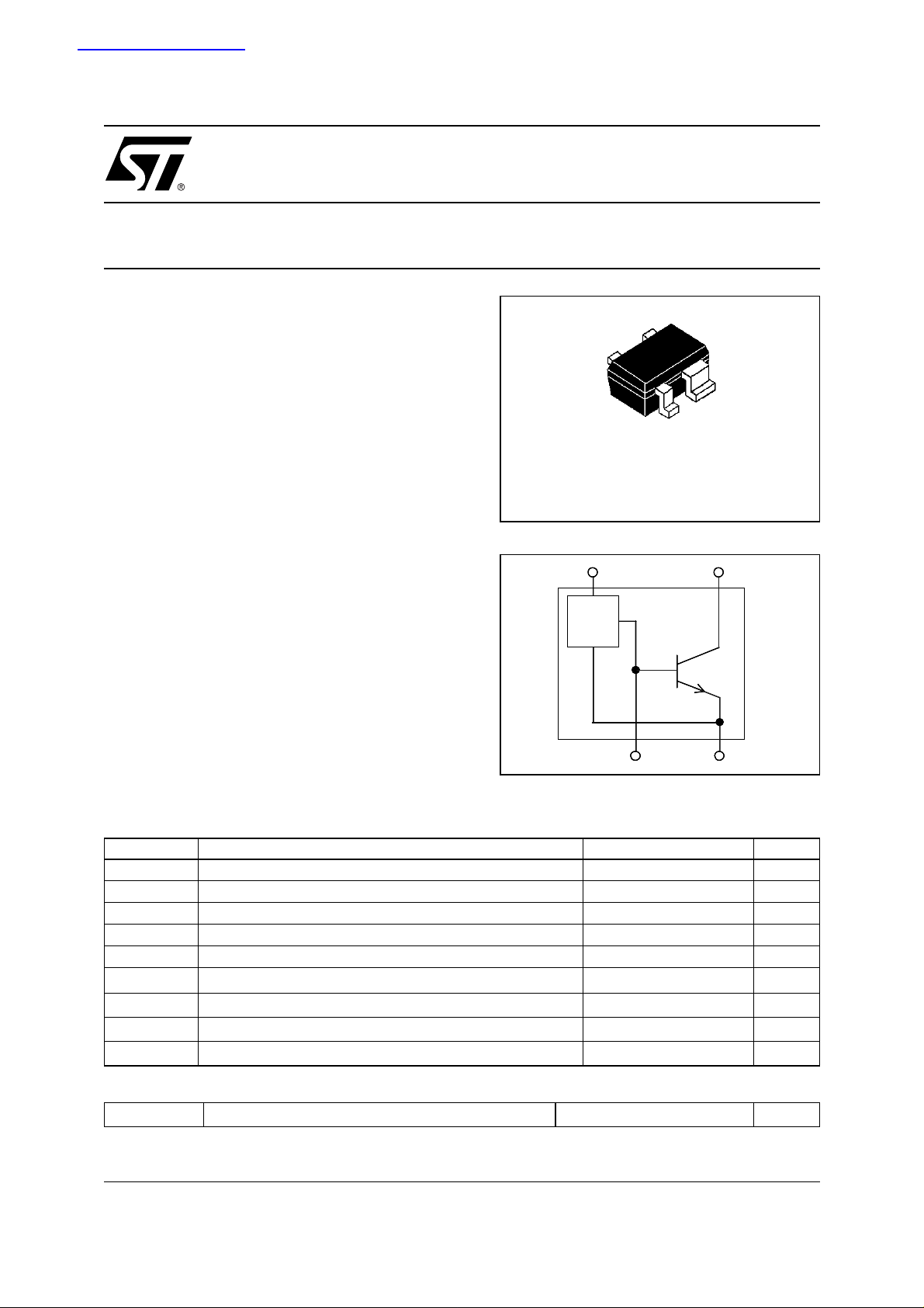
DESCRIPTION
The SMA540B is a NPN Transistor integrating a current mirror as biasing. In this way the IC (collector
current) can be controlled setting the current at Bias
pin according to IC = 10 * IBIAS. The IBIAS current
is easy adjustable using an external resistor.
SMA540B is housed in ultra miniature SOT323-4L
package(LEAD FREE), the rel ative dimensions a re
1.15mmx1.8mm with 0.8mm thickness.
SMA540B
Active Biased RF Transistor
PRELIMINARY DATA
SOT323-4L (SC70)
ORDER CODE
SMA540BTR
Bias
Bias
Bias
Bias, 4
Bias, 4
Bias, 4
B, 1 E, 2
B, 1 E, 2
B, 1 E, 2
BRANDING
TBD
C, 3
C, 3
C, 3
ABSOLUTE MAXIMUM RATINGS
Symbol Parameter Value Unit
V
V
I
BIAS
P
T
T
T
ceo
ebo
I
c
I
b
tot
op
stg
j
Collector emitter voltage 4.5 V
Emitter base voltage 1.5 V
Collector current 40 mA
Base current 4 mA
BIAS Current 4 mA
Total dissipation, Ts = 107 oC
Operating temperature -40 to +85
Storage temperature -65 to +150
Max. operating junction temperature 150
120 mW
THERMAL RESISTANCE
R
thjs
January, 15 2003
Thermal Resistance Junction soldering point < 270
o
C/W
o
C
o
C
o
C
1/4
SMA540B
w
ELECTRICAL CHARACTERISTICS
(T
=25 oC,Z
A
Symbol Parameter Test Conditions Min. Typ. Max. Unit
(1)
Gms
2
|S21|
F
50Ω
P
-1dB
OIP3 Ouput third order intercept point Vd = 2V, Ic = 20mA
C
CB
CR Current Ratio (Ic/I
Note(1): Gms = | S21 / S12 |
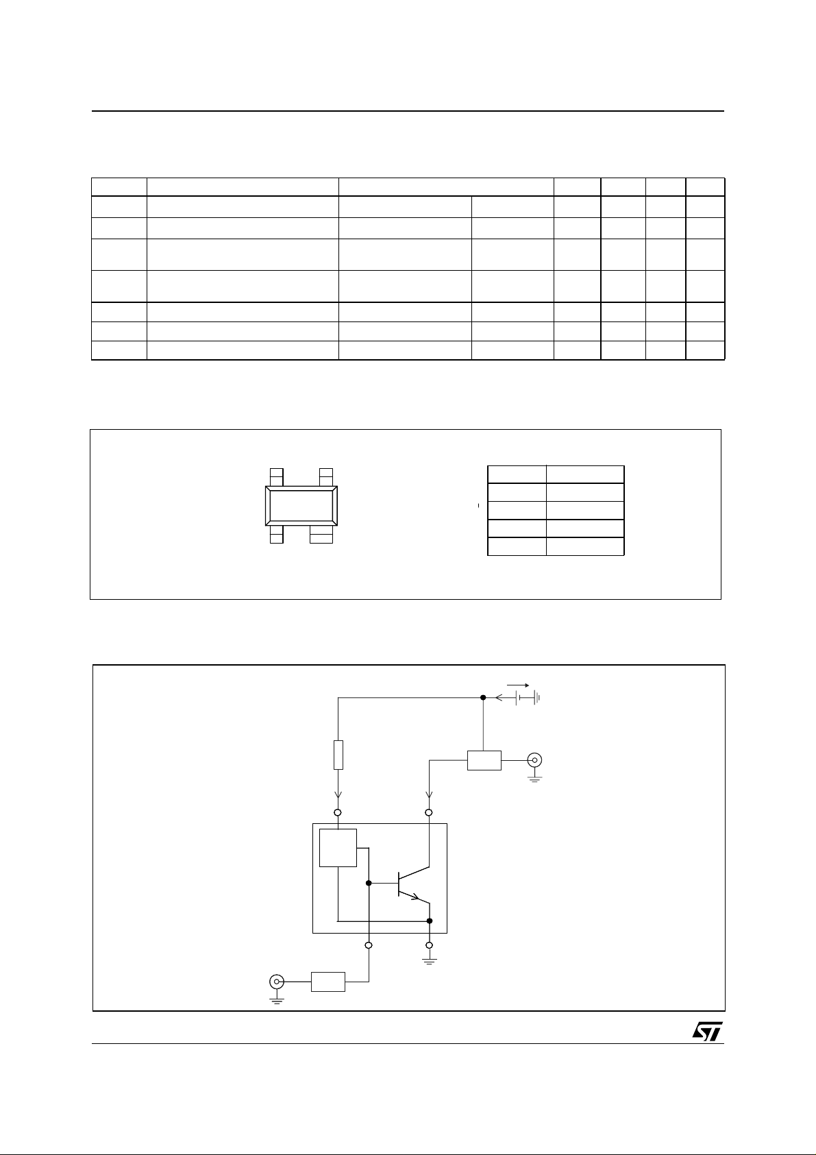
PIN CONNECTION
= 50Ω, tested in circuit shown in fig.1, unless otherwise specified )
L/S
Maximum stable gain Vd = 2V, Ic = 20mA f = 1.8GHz 19 dB
Insertion power gain Vd = 2V, Ic = 20mA f = 1.8GHz 17.5 dB
Noise Figure
Output Power at 1dB
Compression Point
Vd = 2V, Ic = 5mA,
Zs = 50Ω
Vd = 2V, Ic = 20mA,
f = 1.8GHz 1.3 dB
f = 1.8GHz
f = 1.8GHz
9 dBm
19 dBm
Collector-base capacitance Vcb = 2V, f = 1MHz 0.13 pF
)I
Bias
= 0.5mA, Vd = 2V
Bias
10
4
12
SOT343
Typical co nf ig uration (Fig. 1)
SOT343
Bias
Bias
Bias
3
R
I
Bias, 4
Bias, 4
Bias, 4
Bias
Bias
Top vie
I
C
C, 3
C, 3
C, 3
Pin No. Description
1 BASE
2 EMITTER
3 COLLECTOR
4BIAS
V
D
I
D
RF Out
Bias-T
2/4
RF In
N.C.
Bias-T
B, 1 E, 2
B, 1 E, 2
B, 1 E, 2
 Loading...