

ANALOG MULTIPLEXER/DEMULTIPLEXER
■ LOW POWER DISSIPATION:
I
=4µA(MAX.)atTA=25°C
CC
■ LOGIC LEVEL TRANSLATION TO ENABLE
TTL LO GIC SIGNAL TO COMMUNICATE
WITH±5V ANALOG SIGNAL
■ LOW "ON" RESISTANCE:
70ΩTYP. (V
50ΩTYP. (V
■ WIDE ANALOG INPUT VOLTAGE RANGE:
CC-VEE
CC-VEE
±6V
■ FAST SWITCHING:
t
= 13ns (TYP.) at TA=25°C
pd
■ LOW CROSSTALK BETWEEN SWITCHES
■ HIGHON/OFF OUTPUTVOLTAGERATIO
■ WIDE OPERATING SUPPLYVOLTAGE
RANGE (V
■ LOW SINE WAVE DISTORTION:
0.02%atV
■ COMPATIBLE WITH TTL OUTPUTS:
=2V(MIN.)VIL= 0.8V (MAX.)
V
IH
■ PIN AND FUNCTION COMPATIBLE WITH
CC-VEE
CC-VEE
74 SERIES 4051
DESCRIPTION
The M74HCT4051 is a single eight-channel
analog MULTIPLEXER/DEMULTIPLEXER
fabricated with silicon gate C
and it is pin to pin compatible with t he equivalent
metal gate C MOS4000B series.
It c onta ins 8 bidirectional and digitally controlled
analog switches.
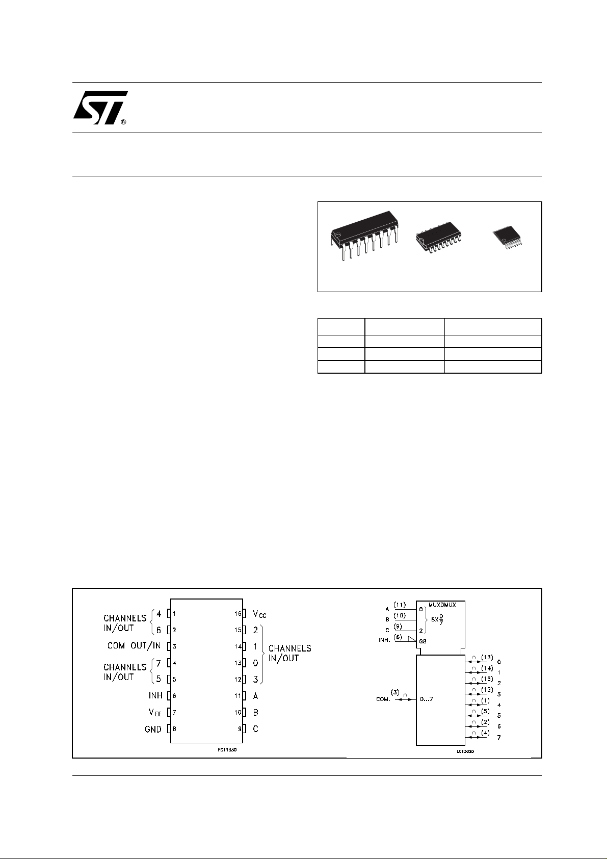
PIN CONNE CTION AND IEC LOGIC SYMBOLS
=4.5V)
=9V)
) = 2 V TO 12V
=9V
2
MOS technology
M74HCT4051
SINGLE 8-CHANNEL
TSSOPDIP SOP
ORDER CODES
PACKAGE TUBE T & R
DIP
SOP
TSSOP
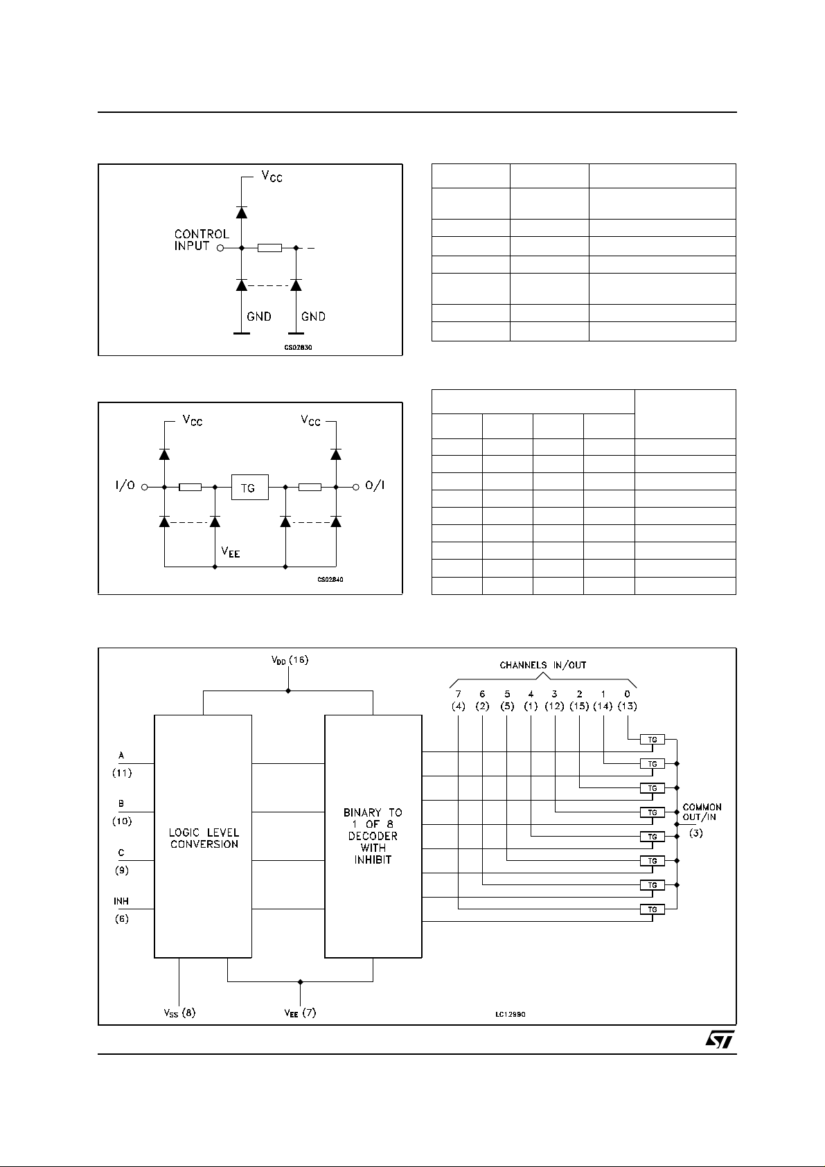
A built-in level shifting is included to allow an input
rangeupto±6V (peak) for an analog signal with
digital control signal of 0 to 6V.
V
EE
signals. It has an inhibit (INH) input terminal to
disable all the switches when high, com pat ibl e
with TTL out put level. For operation as a digital
multiplexer/demultiplexer, VEE is connected to
GND. A, B and C control inputs select one c hannel
out of eight channels; they are compatible with
TTL output level.
All inputs are equipped with protection circuits
against static discharge and transient excess
voltage.
M74HCT4051B1R
M74HCT4051M1R M74HCT4051RM13TR
M74HCT4051TTR
supply pin is provided for analog input
1/14March 2003
M74HCT4051
CONTROL INPUT EQUIVALENT CIRCUIT
I/O EQUIVALENT CIRCUIT
PIN DESCRIPTION
PIN No SYMBOL NAME AND FUNCTION
3COM
OUT/IN
6 INH INHIBIT Input
7V
11, 10, 9 A, B, C Select Inputs
13, 14, 15,
12, 1,5,2,4
8 GND Ground (0V)
16 V
EE
0 to 7 Independent Input/Out-
CC
Common Output/Input
Negative Supply Voltage
puts
Positive Supply Voltage
TRUTH TABLE
INPUT STATE
INH C B A
LLLL 0
LLLH 1
LLHL 2
LLHH 3
LHLL 4
LHLH 5
LHHL 6
LHHH 7
H X X X NONE
ON CHANNEL
FUNCTIONAL DIAGRAM
2/14
M74HCT4051
ABSOLUTE MAXIMUM RATINGS
Symbol Parameter Value Unit
V
V
CC -VEE
V
V
I
CK
I
IOK
I
or I
I
CC
P
T
T
Absolute Maximum Ratings are those values beyond which damage to the device may occur. Functional operation under these conditions is
not implied
(*) 500mWat65
RECOMMENDED OPERATING CONDITIONS
Symbol Parameter Value Unit
V
V
V
CC-VEE
V
V
T
t
r,tf
Supply Voltage
CC
Supply Voltage
Control Input Voltage -0.5 to VCC+ 0.5
I
Switch I/O Voltage VEE-0.5 to VCC+0.5
I/O
Control Input Diode Current
I/O Diode Current
Switch Through Current
T
DC VCCor Ground Current
GND
Power Dissipation
D
Storage Temperature
stg
Lead Temperature (10 sec)
L
°C; derate to 300mW by 10mW/°Cfrom65°Cto85°C
Supply Voltage
CC
Supply Voltage
EE
Supply Voltage
Input Voltage 0 to V
I
I/O Voltage VEEto V
I/O
Operating Temperature
op
Input Rise and Fall Time VCC= 4.5 to 5.5V
-0.5 to +7 V
-0.5 to +13 V
± 20 mA
± 20 mA
± 25 mA
± 50 mA
500(*) mW
-65 to +150 °C
300 °C
4.5 to 5.5 V
-6 to 0 V
2to12 V
CC
CC
-55 to 125 °C
0 to 500 ns
V
V
V
V
3/14
M74HCT4051
DC SPECIFICATIONS
Test Condition Value
Symbol Parameter
V
V
R
∆R
High Level Input
IHC
Voltage
Low Level Input
ILC
Voltage
ON Resistance 4.5 GND VI=V
ON
Difference of ON
ON
Resistance
between switches
I
Input/Output
OFF
Leakage Current
(SWITCH OFF)
Switch Input
I
IZ
Leakage Current
(SWITCH ON,
OUTPUT OPEN)
I
Input L eakage
I
Current
I
Quiescent Supply
CC
Current
∆I
Additional
CC
Quiescent Supply
Current per input
pin
V
(V)
CC
V
(V)
EE
= 25°C
T
A
-40 to 85°C
Min. Typ. Max. Min. Max. Min. Max.
-55 to
125°C
4.5
to
2.0 2.0 2.0 V
5.5
4.5
to
0.8 0.8 0.8 V
5.5
or V
IHC
V
4.5 -4.5 55 120 150 180
4.5 G ND V
4.5 -4.5 50 100 125 150
4.5 G ND V
4.5 -4.5 5 12 15 18
I/O=VCC
I
I/O
I=VIHC
V
I/O=VCC
I
I/O
I=VIHC
V
I/O=VCC
I
I/O
≤ 2mA
≤ 2mA
≤ 2mA
to V
or V
or V
or V
or V
ILC
EE
ILC
EE
ILC
EE
5.5 G ND VOS=VCCor GND
V
= GND or V
5.5 -6.0
5.5 G ND V
5.5 -6.0
IS
VI=V
ILC
OS=VCC
V
I=VIHC
or V
or GND
or V
CC
IHC
ILC
85 180 225 270
70 150 190 230
10 30 35 45
±
0.06
± 0.6 ± 1.0
± 0.1 ± 1 ± 1
±
0.06
± 0.6 ± 1.0
± 0.1 ± 1 ± 1
5.5 G ND VI=VCCor GND ± 0.1 ± 0.1 ± 1
5.5 G ND
5.5 -6.0 8 80 160
4.5
to
GND
V
I=VCC
V
other inp ut at V
5.5
I=VCC
or GND
or GND
- 2.1V
CC
100 360 450 490 µA
44080
Unit
Ω
Ω
µA
µA
µA
µA
4/14
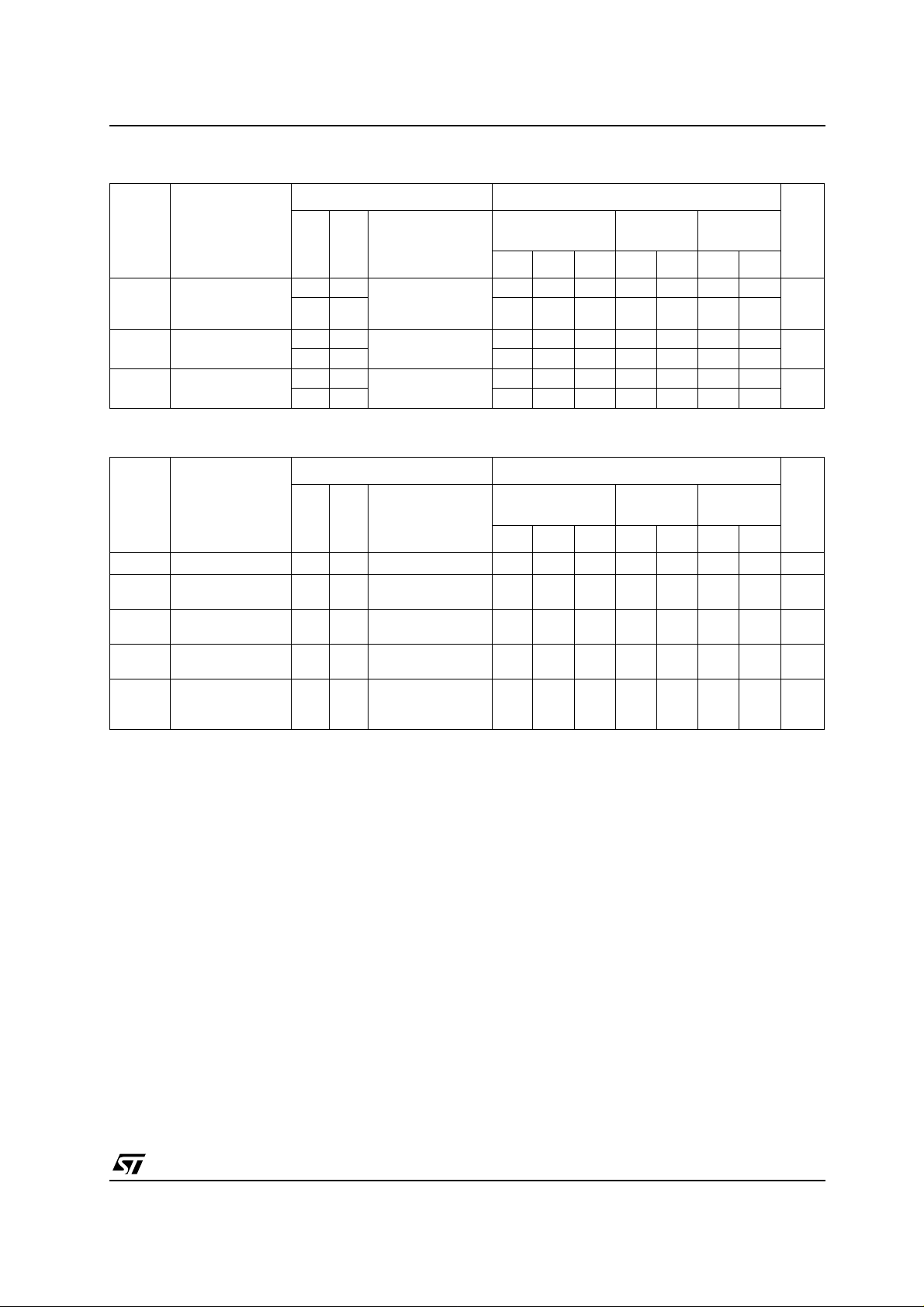
AC ELECTRICAL CHARACTERISTICS (CL= 50 pF, Input tr=tf=6ns)
Test Condition Value
M74HCT4051
Symbol Parameter
Φ
Phase Difference
I/O
Between Input and
Output
PZL
PZH
PLZ
PHZ
Output Enable
Time
Output Disable
Time
t
t
t
t
= 25°C
T
V
V
CC
EE
(V)
(V)
4.5 GND
= 50pF
C
4.5 -4.5 4 8 10 12
L
4.5 GND RL=1KΩ
C
4.5 -4.5 11 34 43 51
= 50pF
L
4.5 GND RL=1KΩ
C
4.5 -4.5 19 31 39 47
= 50pF
L
A
Min. Typ. Max. Min. Max. Min. Max.
512 15 18
13 45 56 68
25 38 48 58
-40 to 85°C
-55 to
125°C
Unit
ns
ns
ns
CAPACITANCE CHARACTERISTICS
Test Condition Value
Symbol Parameter
V
(V)
CC
V
(V)
EE
T
A
-40 to 85°C
= 25°C
Min. Typ. Max. Min. Max. Min. Max.
Input Capacitance 5.0 5 10 10 10 pF
C
IN
C
C
C
C
Common Terminal
I/O
Capacitance
Switch Terminal
I/O
Capacitance
Feed Through
IOS
Capacitance
Power Dissipation
PD
Capacitance
5.0 -5.0 11 20 20 20 pF
5.0 -5.0 7 15 15 15 pF
5.0 -5.0 0.75 2 2 2 pF
5.0 GND 67 pF
(note 1)
1) CPDis defined as the value of the IC’s internal equivalent capacitance which is calculated from the operating current consumption without
load. (Refer to Test Circuit). Average operating current can be obtained by the following equation. I
CC(opr)=CPDxVCCxfIN+ICC
-55 to
125°C
Unit
5/14

M74HCT4051
ANALOG S WITCH CHARACTERISTICS (GND = 0V;TA=25°C)
Symbol Parameter Test Condition Value Unit
V
V
CC
(V)
V
(V)
EE
(V
IN
p-p
)
Typ.
Sine Wave
Distortion
Sine Wave
Distortion
f
MAX
Frequency
Response
(Switch ON) (*)
MAX
Frequency
Response
f
(Switch ON) (**)
Feed through
Attenuation
(Switch OFF)
Crosstalk (Control
Input to Signal
Output)
Crosstalk
(between any two
switches)
(*) Input COMMON Terminal, and measured at SWITCH Terminal
(**) Input SWITCH Terminal, and measured at common Terminal
NOTE: These characteristics are determined by the design of the device.
2.25 -2.25 4
4.5 -4.5 8 0.020
2.25 -2.25 4
4.5 -4.5 8 0.06
f
2.25 -2.25 Adjust f
Increase f
IN
R
=50Ω,CL=10pF,fIN= 1KHz sine wave
L
2.25 -2.25 Adjust fINvoltage to obtain 0 dBm at VOS.
Increase f
6.0 -6.0
IN
R
=50Ω,CL=10pF,fIN= 1KHz sine wave
L
2.25 -2.25 V
4.5 -4.5 -50
= 600Ω,CL=50pF,fIN= 1MHz sine wave
R
L
4.5 0 Adjust R
R
4.5 -4.5 140
=600Ω,CL=50pF,fIN= 1MHz square wave between
L
2.25 -2.25 Adjust V
R
4.5 -4.5 -50
= 600Ω,CL=50pF,fIN= 1MHz sine wave
L
= 1 KHz RL=10KΩ,CL=50pF
f
IN
=10KHzRL=10KΩ,CL=50pF
IN
voltage to obtain 0 dBm at VOS.
IN
Frequency until dB meter reads -3dB
Frequency until dB meter reads -3dB
is centered at (VCC-VEE)/2
IN
Adjust input for 0 dBm
at set up so that IS=0A.
L
Vcc and GND tr=tf= 6 ns
to obtain 0dBm at input
IN
0.025
0.12
120
95
-50
60
-50
%
%
MHz4.5 -4.5 190
MHz4.5 -4.5 150
dB
mV
dB
6/14

M74HCT4051
SWITCHING CARACTERISTICS TEST CIRCUIT
CROSSTALK (control to output)
BANDWIDTH AND FEEDTHROUGH ATTENUATION CROSSTALK BETWEEN ANY TWO SWITCHES
7/14

M74HCT4051
SWITCHING CHAR ACTERISTICS WAVEFORM
CHANNEL RESISTANCE (R
8/14
ON)
ICC(Opr.)

M74HCT4051
Plastic DIP-16 (0.25) MECHANICAL DATA
mm. inch
DIM.
MIN. TYP MAX. MIN. TYP. MAX.
a1 0.51 0.020
B 0.77 1.65 0.030 0.065
b 0.5 0.020
b1 0.25 0.010
D 20 0.787
E 8.5 0.335
e 2.54 0.100
e3 17.78 0.700
F 7.1 0.280
I 5.1 0.201
L 3.3 0.130
Z 1.27 0.050
P001C
9/14

M74HCT4051
SO-16 MECHANICAL DATA
DIM.
A 1.75 0.068
a1 0.1 0.2 0.004 0.008
a2 1.65 0.064
b 0.35 0.46 0.013 0.018
b1 0.19 0.25 0.007 0.010
C 0.5 0.019
c1 45˚ (typ.)
D 9.8 10 0.385 0.393
E 5.8 6. 2 0.228 0.244
e 1.27 0.050
e3 8.89 0.350
F 3.8 4.0 0. 149 0.157
G 4.6 5.3 0. 181 0.208
L 0.5 1.27 0.019 0.050
M 0.62 0.024
S8 ˚ (max.)
MIN. TYP MAX. MIN. TYP. MAX.
mm. inch
10/14
PO13H

M74HCT4051
TSSOP16 MECHANICAL DATA
mm. inch
DIM.
MIN. TYP MAX. MIN. TYP. MAX.
A 1.2 0.047
A1 0.05 0.15 0.002 0.004 0.006
A2 0.8 1 1.05 0.031 0.039 0.041
b 0.19 0.30 0.007 0.012
c 0.09 0.20 0.004 0.0079
D 4.9 5 5.1 0.193 0.197 0.201
E 6.2 6.4 6.6 0.244 0.252 0.260
E1 4.3 4.4 4.48 0.169 0.173 0.176
e 0.65 BSC 0.0256 BSC
K0˚ 8˚0˚ 8˚
L 0.45 0.60 0.75 0.018 0.024 0.030
A2
A
A1
b
e
c
K
L
E
D
E1
PIN 1 IDENTIFICATION
1
0080338D
11/14

M74HCT4051
Tape & Reel SO-16 MECHANICAL DATA
mm. inch
DIM.
MIN. TYP MAX. MIN. TYP. MAX.
A 330 12.992
C 12.8 13.2 0.504 0.519
D 20.2 0.795
N 60 2.362
T 22.4 0.882
Ao 6.45 6.65 0.254 0.262
Bo 10.3 10.5 0.406 0.414
Ko 2.1 2.3 0.082 0.090
Po 3.9 4.1 0.153 0.161
P 7.9 8.1 0.311 0.319
12/14

M74HCT4051
Tape & Reel TSSOP16 MECHANICAL DATA
mm. inch
DIM.
MIN. TYP MAX. MIN. TYP. MAX.
A 330 12.992
C 12.8 13.2 0.504 0.519
D 20.2 0.795
N 60 2.362
T 22.4 0.882
Ao 6.7 6.9 0.264 0.272
Bo 5.3 5.5 0.209 0.217
Ko 1.6 1.8 0.063 0.071
Po 3.9 4.1 0.153 0.161
P 7.9 8.1 0.311 0.319
13/14

M74HCT4051
Information furnished is believed to be accurate and reliable . However, STMicroelectronics assumes no responsibility for the
consequences of use o f suc h inf ormat ion n or f or an y infr ingeme nt of paten ts or oth er ri gh ts of third part ies whic h may resul t f rom
its use. No license is granted by implication or otherwise under any patent or patent rights of STMicroelectronics. Specifications
mentioned in this publication are subject to change without notice. This publication supersedes and replaces all information
previously supplied. STMicroelectronics products are not authorized for use as critical components in life support devices or
systems without express written approval of STMicroelectronics.
Australia - Brazil - Canada - China - Finland - France - Germany - Hong Kong - India - Israel - Italy - Japan - Malaysia - Malta - Morocco
© The ST logo is a registered trademark of STMicroelectronics
© 2003 STMicroelectronics - Printed in Italy - All Rights Reserved
STMicroelectronics GROUP OF COMPANIES
Singapore - Spain - Sweden - Switzerland - United Kingdom - United States.
© http://www.st.com
14/14
 Loading...