

Page 1
February 1998 1/49
R
ST624x-KIT
STARTER KIT FOR ST624x MCU FAMILY
HARDWARE FEATURES
■
Immediate evaluation of ST6240 with
demonstration examples
■
Program debugging within the user’s real
application environment
■
On board programming of ST62E46 and
ST62T46
■
In-circuit programming of ST62E4x and
ST62T4x devices on the user’s application
board
SOFTWARE FEATURES
■
Software simulator including LCD display and
I/O read/write
■
Assembler, linker, debugger
■
EPROM/OTP programming utilities
■
Application examples
5
查询ST624x-KIT供应商 捷多邦,专业PCB打样工厂,24小时加急出货
Page 2

2/49
Table of Contents
6
ST624x -KIT . . . . . . . . . . . . . . . . . . . . . . . . . . . . . . . . . . . . . . . . . 1
1 INTRODUCTION . . . . . . . . . . . . . . . . . . . . . . . . . . . . . . . . . . . . . . . . . . . . . . . . . . . . . . . . . . . . . . 4
1.1 Where to go from here... . . . . . . . . . . . . . . . . . . . . . . . . . . . . . . . . . . . . . . . . . . . . . . . . . . . 7
2 THE STARTER KIT HARDWARE . . . . . . . . . . . . . . . . . . . . . . . . . . . . . . . . . . . . . . . . . . . . . . . . . 8
2.1 The ST6 Microcontroller . . . . . . . . . . . . . . . . . . . . . . . . . . . . . . . . . . . . . . . . . . . . . . . . . . . . 8
2.2 The Starter Kit Board . . . . . . . . . . . . . . . . . . . . . . . . . . . . . . . . . . . . . . . . . . . . . . . . . . . . . . 8
2.3 8 MHz and 32 KHz Oscillators . . . . . . . . . . . . . . . . . . . . . . . . . . . . . . . . . . . . . . . . . . . . . . 12
2.4 8-alphanumeric Digit LCD . . . . . . . . . . . . . . . . . . . . . . . . . . . . . . . . . . . . . . . . . . . . . . . . . 12
2.5 Reset Button . . . . . . . . . . . . . . . . . . . . . . . . . . . . . . . . . . . . . . . . . . . . . . . . . . . . . . . . . . . 12
2.6 LED Indicator . . . . . . . . . . . . . . . . . . . . . . . . . . . . . . . . . . . . . . . . . . . . . . . . . . . . . . . . . . . 12
2.7 Hexadecimal Keyboard . . . . . . . . . . . . . . . . . . . . . . . . . . . . . . . . . . . . . . . . . . . . . . . . . . . 12
2.8 Resistance trimmer . . . . . . . . . . . . . . . . . . . . . . . . . . . . . . . . . . . . . . . . . . . . . . . . . . . . . . 14
2.9 Combi-ports PC0-7 . . . . . . . . . . . . . . . . . . . . . . . . . . . . . . . . . . . . . . . . . . . . . . . . . . . . . . 14
3 INSTALLING THE STARTER KIT . . . . . . . . . . . . . . . . . . . . . . . . . . . . . . . . . . . . . . . . . . . . . . . 15
3.1 Hardware and Software Requirements . . . . . . . . . . . . . . . . . . . . . . . . . . . . . . . . . . . . . . . 15
3.2 I ns ta llin g the Softwar e . . . . . . . . . . . . . . . . . . . . . . . . . . . . . . . . . . . . . . . . . . . . . . . . . . . . 15
3.3 Connecting the Power Supply . . . . . . . . . . . . . . . . . . . . . . . . . . . . . . . . . . . . . . . . . . . . . . 15
4 RUNNING THE DEMOS . . . . . . . . . . . . . . . . . . . . . . . . . . . . . . . . . . . . . . . . . . . . . . . . . . . . . . . 17
4.1 What the Demos Do . . . . . . . . . . . . . . . . . . . . . . . . . . . . . . . . . . . . . . . . . . . . . . . . . . . . . . 17
4.1.1 Demo 1 - Key Display . . . . . . . . . . . . . . . . . . . . . . . . . . . . . . . . . . . . . . . . . . . . . . . 17
4.1.2 Demo 2 - Voltmeter . . . . . . . . . . . . . . . . . . . . . . . . . . . . . . . . . . . . . . . . . . . . . . . . . 17
4.2 Running the Demonstration Programs . . . . . . . . . . . . . . . . . . . . . . . . . . . . . . . . . . . . . . . . 18
5 CONNECTING EXTERNAL RESOURCES TO THE STARTER KIT BOARD . . . . . . . . . . . . . . 19
6 USING THE STARTER KIT BOARD AS A HARDWARE SIMULATOR . . . . . . . . . . . . . . . . . . 22
6.1 The Data Transmission Driver . . . . . . . . . . . . . . . . . . . . . . . . . . . . . . . . . . . . . . . . . . . . . . 23
6.2 Technical Limitations . . . . . . . . . . . . . . . . . . . . . . . . . . . . . . . . . . . . . . . . . . . . . . . . . . . . . 23
6.3 Error Messages . . . . . . . . . . . . . . . . . . . . . . . . . . . . . . . . . . . . . . . . . . . . . . . . . . . . . . . . . 25
6.4 Troublesho oting . . . . . . . . . . . . . . . . . . . . . . . . . . . . . . . . . . . . . . . . . . . . . . . . . . . . . . . . . 25
7 EXERCISES . . . . . . . . . . . . . . . . . . . . . . . . . . . . . . . . . . . . . . . . . . . . . . . . . . . . . . . . . . . . . . . . 26
7.1 Exercise 1 . . . . . . . . . . . . . . . . . . . . . . . . . . . . . . . . . . . . . . . . . . . . . . . . . . . . . . . . . . . . . 26
7.2 Exercise 2 . . . . . . . . . . . . . . . . . . . . . . . . . . . . . . . . . . . . . . . . . . . . . . . . . . . . . . . . . . . . . 30
8 PROGRAMMING ST6 MICROCONTROLLERS . . . . . . . . . . . . . . . . . . . . . . . . . . . . . . . . . . . . . 32
8.1 Setting Up the Starter Kit Board . . . . . . . . . . . . . . . . . . . . . . . . . . . . . . . . . . . . . . . . . . . . . 32
8.2 In-Circuit Programming . . . . . . . . . . . . . . . . . . . . . . . . . . . . . . . . . . . . . . . . . . . . . . . . . . . 33
8.2.1 Application B oard Connect ions . . . . . . . . . . . . . . . . . . . . . . . . . . . . . . . . . . . . . . . . 33
8.3 Setting Up the Starter Kit Board for In-Circuit Programming . . . . . . . . . . . . . . . . . . . . . . . 35
Page 3

3/49
Table of Contents
9 LCD INTERFACE . . . . . . . . . . . . . . . . . . . . . . . . . . . . . . . . . . . . . . . . . . . . . . . . . . . . . . . . . . . . 36
9.1 ST6240 LCD DRIVER OVERVIE W . . . . . . . . . . . . . . . . . . . . . . . . . . . . . . . . . . . . . . . . . . 36
9.2 STARTER KIT LCD PANEL INTERFACE . . . . . . . . . . . . . . . . . . . . . . . . . . . . . . . . . . . . . 37
9.3 Interfacing The LCD Panel with the ST6240 LCD Driver . . . . . . . . . . . . . . . . . . . . . . . . . . 40
9.4 Character Definition Examples . . . . . . . . . . . . . . . . . . . . . . . . . . . . . . . . . . . . . . . . . . . . . . 42
9.4.1 Character A Definition . . . . . . . . . . . . . . . . . . . . . . . . . . . . . . . . . . . . . . . . . . . . . . . 42
9.4.2 Character 3 Definition . . . . . . . . . . . . . . . . . . . . . . . . . . . . . . . . . . . . . . . . . . . . . . . 43
9.5 Starter Kit LCD Panel Character Set Software Model . . . . . . . . . . . . . . . . . . . . . . . . . . . . 44
9.5.1 Direct Code LCD RAM Patching . . . . . . . . . . . . . . . . . . . . . . . . . . . . . . . . . . . . . . . 44
9.5.2 Indexed Data ROM . . . . . . . . . . . . . . . . . . . . . . . . . . . . . . . . . . . . . . . . . . . . . . . . . 44
9.5.3 Complete Message Displa y . . . . . . . . . . . . . . . . . . . . . . . . . . . . . . . . . . . . . . . . . . 45
10 HARDWARE INFORMATION . . . . . . . . . . . . . . . . . . . . . . . . . . . . . . . . . . . . . . . . . . . . . . . . . . 47
10.1Part List . . . . . . . . . . . . . . . . . . . . . . . . . . . . . . . . . . . . . . . . . . . . . . . . . . . . . . . . . . . . . . . 47
10.2Starter Kit Board Schematic . . . . . . . . . . . . . . . . . . . . . . . . . . . . . . . . . . . . . . . . . . . . . . . . 47
7
Page 4

4/49
Introduction
1 INTRODUCTION
The ST624x Starter Kit provides you with all you need to start designing, developing and evaluating programs for ST624x microcontrollers immediately.
The ST624x Starter Kit includes:
• The ST6 assembler and linker, AST6 and LST6.
• The ST6 Windows debugger, WGDB6.
• The Windows ST6 microcontroller programmer, Epromer.
• The ST6 Starter Kit board, w hich serves as a demonstration board and low-cost debugging tool.
• Some demonstration programs that show how ST6 microcontrollers use the Starter Kit
board resources.
• Some example programs.
• Two ST62E46BF1 microcontro llers.
• A complete set of paper documentation and online help.
The demonstration programs, that come pre-loaded on the ST62T40B microcontroller, show
how the powerful features of ST6 microcontrollers operate in a real environment. The demonstration programs use the hardware resources provided on the Starter Kit board, which include an LCD, hexadecimal keyboard, a resistance trimmer and an 8 MHz and a 32 KHz oscillator.
Using the ST6 assembler and linker, AST6 and LST6, you can assemble and link ST6 programs. The "ST6 Family Software development tools AST6, LST6, WGDB6" User Manual will
guide you through the steps of developing, assembling and linking programs for the ST6. The
Starter Kit software includes a set of example programs of typical ST6 applications. These are
installed in the directory C:\st6tools\sk624Xi1\examples.
For a fast-track solution for developing bug-free programs for the ST6, without the hassle of
writing assembler code, try out the ST6-Realizer program.
Once you have developed your ST6 program, you can use the Windows-based ST6 program
debugger, WGDB6/SIMULATOR, together with the Starter Kit board, as a low-cost but powerful debugging tool. WGDB6 includes an ST6 simulator, that simulates the execution of your
program, and uses the ST6 that is plugged into the Starter Kit board to emulate all transactions that are performed with the data space. Thus, using the Starter Kit board with WGDB6,
you can view how the microcontroller peripherals behave when your program is executed.
WGDB6 includes powerful debugging features, such as source-level debugging, instruction
and conditional memory access breakpoints and selective trace recording. The "ST 6 Family
8
Page 5

5/49
Introduction
Software development tools AST6, LST6, WGDB6" User Manual and online help will lead you
through the debugging process using WGDB6.
When your program is ready, Epromer provides you with an easy-to-use Windows interface,
which lets you prepare executable code, then write it to the ST62E46B microcontroller that
can be plugged into the SDIP56 ZIF socket on the Starter Kit board, or your own in-circuit application board that is connected to the Starter Kit board.
The ST62T40B can’t be erased or programmed, it is already programmed and contains the
demonstrations program.
To observe and evaluate the consequences of your program on the resources it controls, you
can run it on the ST62T40B microcontroller that is s oldered on the Starter K it board in Hardware Simulation mode. If it controls a resource that is not included on the Starter Kit board,
you can connect your own resource to the board.
Instructions for use - Warning
This product conforms with the 89/336/EEC directive; it also complies with the EN55022 emissions standard for ITE, as well as with generic 50082-1 immunity standards.
The product is a
Class A apparatus
. In a residential environment this device may cause ra-
dioelectrical disturbances which may require that the user adopt appropriate precautions.
The product is not contained in an outer c asing, and cannot therefore be immune against elec-
trostatic discharge (ESD):
it should therefore only be handled at static safe work stations.
9
Page 6
6/49
Introduction
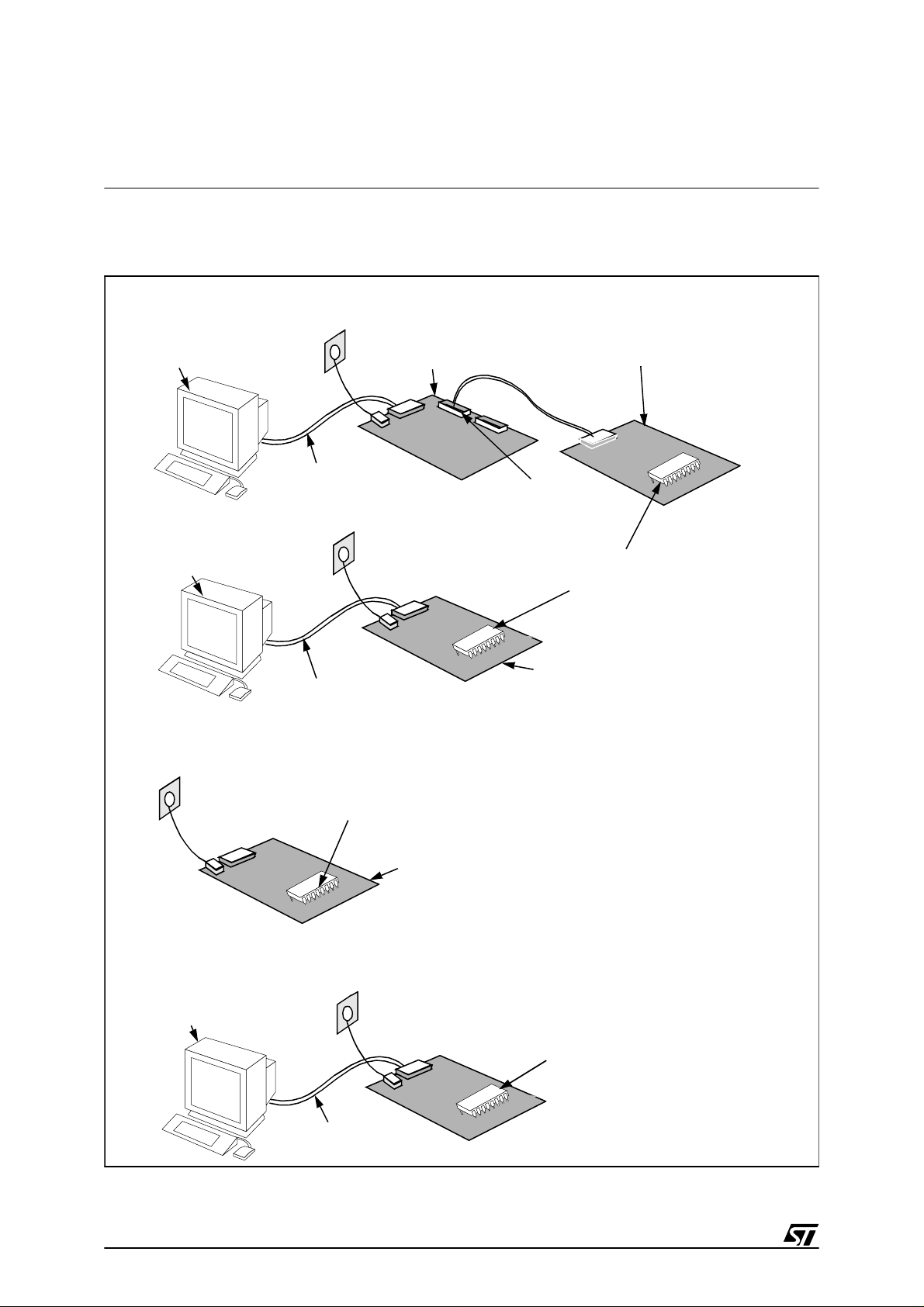
The following diagram summarises the possible uses of the Starter Kit board and the hardware setup required for each one.
To program ST6s on your own in-circuit programming board:
To run the demonstrations:
To use the Starter Kit board as a hardware simulator:
To program ST6s using the Starter Kit board:
PC running
Epromer
Starter Kit
board
In-circuit
programming board
Parallel port
connected to P2
Parallel port
connected to P2
P1 connector
ST6 to be
programmed
PC running
Epromer
ST62T40B Programmed with
DEMOKIT2.HEX
Starter Kit board
Starter Kit board
PC running
WGDB6 Simulator
ST62T40B Programmed with
DEMOKIT2.HEX
Parallel port
connected to P2
10
Page 7

7/49
Introduction
1.1 Where to go from here...
The following table directs you to where you should look for further information about using the
ST6 Starter Kit
To: Refer to:
Find out about the Starter Kit board and ST6
microcontrollers provided with the kit.
“The Starter Kit Hardware” on page 8 of this book.
Install the Starter Kit software, and connect the
power supply to th e board.
“Installing the Starter Kit” on page 15 of this book.
Find out what the demonstration applications do,
and run them.
“Running the Demos” on page 17 of this book.
Learn how to develop source code for AST6 and
LST6.
"ST6 Family Software development tools AST 6,
LST6, WGDB6" User Manual.
Prepare the Starter Kit board for use as an ST6
hardware simulator with WGDB6.
“Using The Starter Kit Board as a Hardware
Simulator” on page 22 of this book.
Learn how to use WGDB6 for debugging your
programs.
"ST6 Family Software development tools AST 6,
LST6, WGDB6" User Manual.
Prepare the Starter Kit board for programming
ST6 microcontrollers using Epromer.
“Programming ST6 Microcontrollers” on page 32 of
this book.
Prepare the Starter Kit board for connecting your
own in-circuit programming board.
“In-Circuit Programming” on page 33 of this book.
Learn how to use Eprommer for programming
ST6 microcontrollers.
The Epromer online help.
Connect your own hardware resource or LCD to
the Starter Kit board.
“Connecting External Resources to the Starter Kit
Board” on page 19 of this book.
Perform some introductory excercises using
WGDB6.
“Exercises” on page 26.
Learn how the LCD interface works. “LCD Interface” on page 36.
11
Page 8

8/49
The Starter Kit Hardware
2 THE STARTER KIT HARDWARE
This section describes the ST6 microcontrollers and the Starte r Kit board that come w ith the
ST6 Starter Kit. A full schematic of the Starter Kit board is provided in “Hardware Information”
on page 47.
2.1 The ST6 Microcontroller
The Starter Kit includes two ST62E46BF1 microcontrollers.
The ST62T40B microcontroller is pre-loaded with the c ode
DEMOKIT2.HEX
, which includes
the demonstration programs (see “Running the Demos” on page 17), as well as the communications protocol program, that enables you to use the Starter Kit board as a sim ulator (see
“Using The Starter Kit Board as a Hardware Simulator” on page 22).
2.2 The Starter Kit Board
The Starter Kit board includes the following resources:
• A Reset button.
• An 8-alphanumeric digit LCD.
• A hexadecimal keyboard.
• A LED indicator.
• A resistance trimmer.
• One 8 MHz and one 32 KHz oscillator.
• A SDIP56 ZIF socket to program the ST62E46B or ST62T46B.
It comes with its own power supply unit that can be plugged i nto an AC mains source, or a DC
source with the following characteristics:
• Voltage: 16V min./20V max.
• Current: 100 mA min.
12
Page 9
9/49
The Starter Kit Hardware
It includes the following connectors:
• A parallel port connector (P2) for connection to the host PC when it is used as a hardware
simulator or for programming.
• A remote resource I/O interface (J1).
• An in-circuit ST6 programming board connector (P1).
• A remote LCD connector (J2) to which you can connect your own LCD.
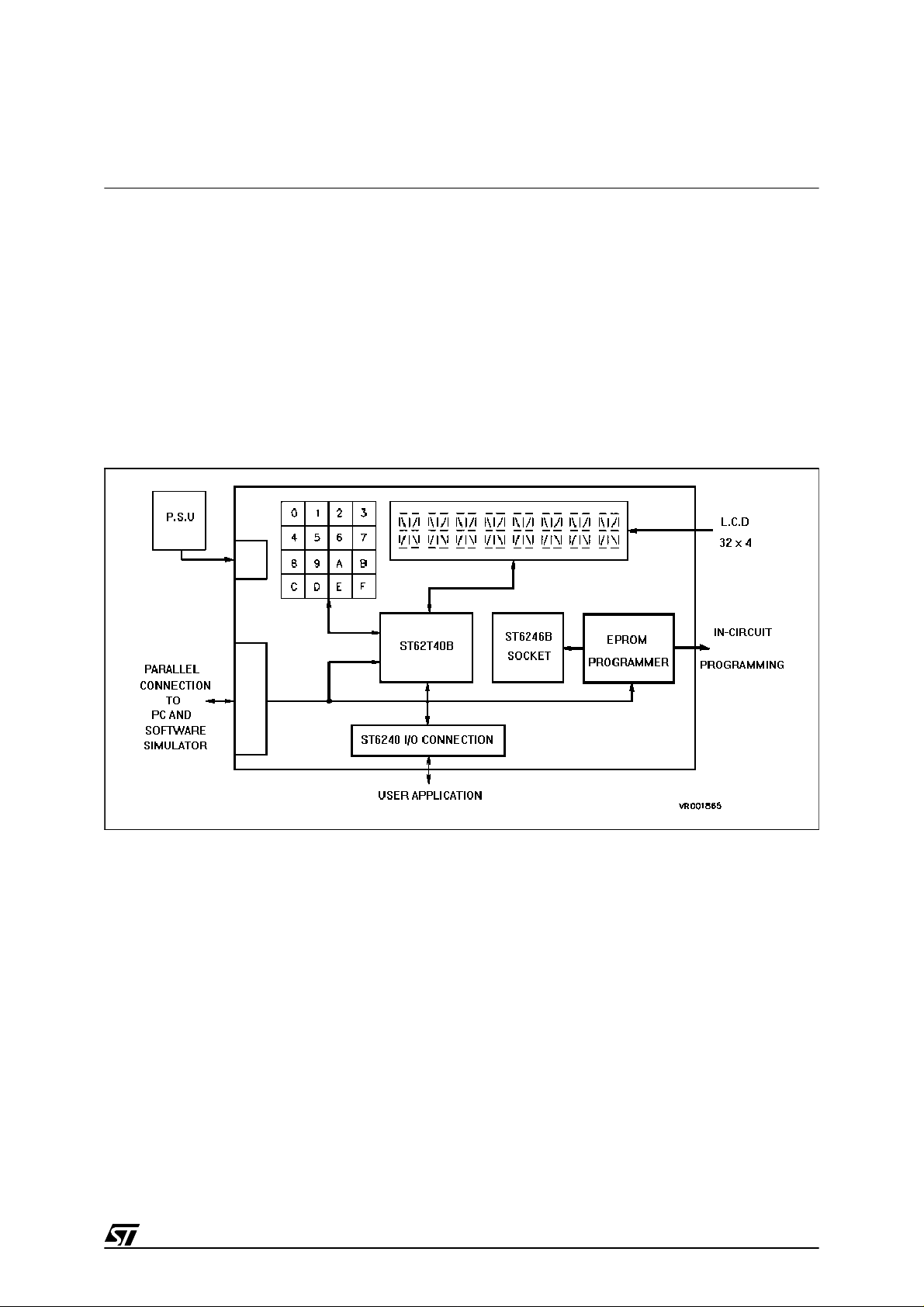
Below is a block diagram of the Starter Kit board:
13
Page 10
10/49
The Starter Kit Hardware
ST624x Starter Kit Board
14
Page 11
11/49
The Starter Kit Hardware
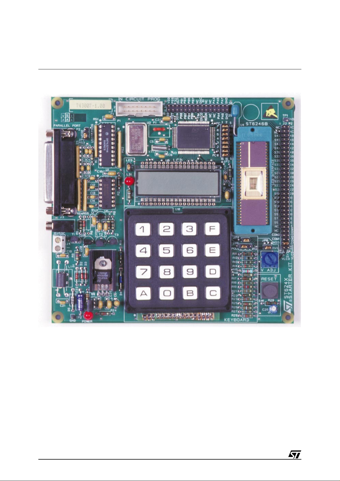
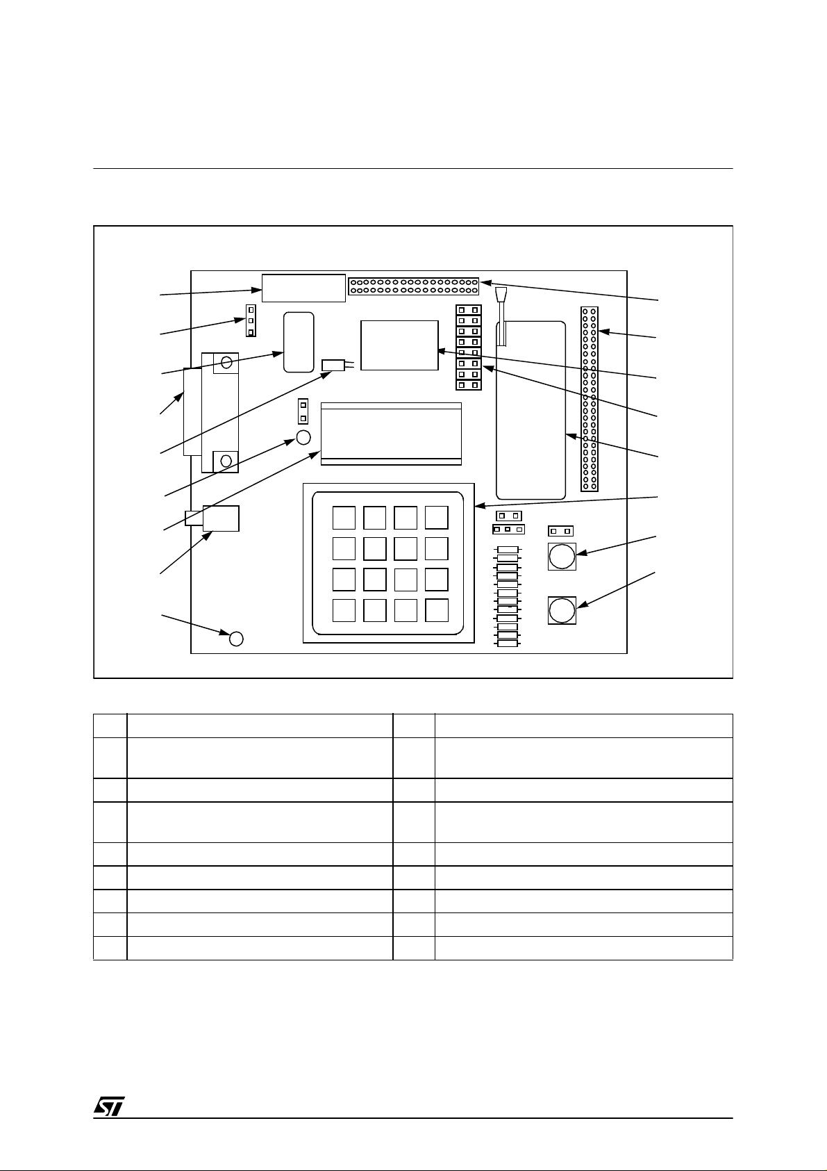
The following diagram shows the layout of the Starter Kit board.
1 In-circuit programming connector P1. 17 Remote resource I/O interface J1.
2 “Programming” or “User” operating mode
selection jumper JP1.
16 Remote LCD interface connector J2.
3 8 Mhz oscillator. 15 ST62T40B MCU
4 PC connector P2. 14 LCD protection with jumper JP2 if the combi-
port PC0-7 is used.
5 32.768 KHz oscillator. 13 SDIP56 ZIF MCU socket.
6 LED indicator LD1. 12 Keyboard
7 LCD display. 11 Voltage trimmer
8 Power supply JACK connector J3. 10 RESET button.
9 Power supply LED indicator LD2.
1
2
3
4
5
6
7
8
9
11
12
13
14
15
16
JP1
17
ST6246B
ST62T40B
SOCKET
DISPLAY
10
F
E654
789D
CB0A
321
15
Page 12
12/49
The Starter Kit Hardware
2.3 8 MHz and 32 KHz Oscillators
An oscillator feeds the ST62T40B OSCIN input with an 8 MHz clock signal.
A 32 KHz oscillator is delivered with the boar d. The required components: crystal XT1 and ca-
pacitors C5, C6 are connected to the ST62T40B as described in the ST6240 Data Book.
2.4 8-alphanumeric Digit LCD
An 8-alphanumeric digit LCD is connected to the ST62T40B LCD driver outputs. It has 32 segments that are driven by 4 COM outputs. You can disconnect a part of the LCD by removing
jumper JP2 if you want to use the combi-port PC0-7 on the connector interface J2. For full details about the LCD see “LCD Interface” on page 36.
2.5 Reset Button
This activates the ST62T40B RESET input when pressed. A power-on reset circuit is also provided.
2.6 LED Indicator
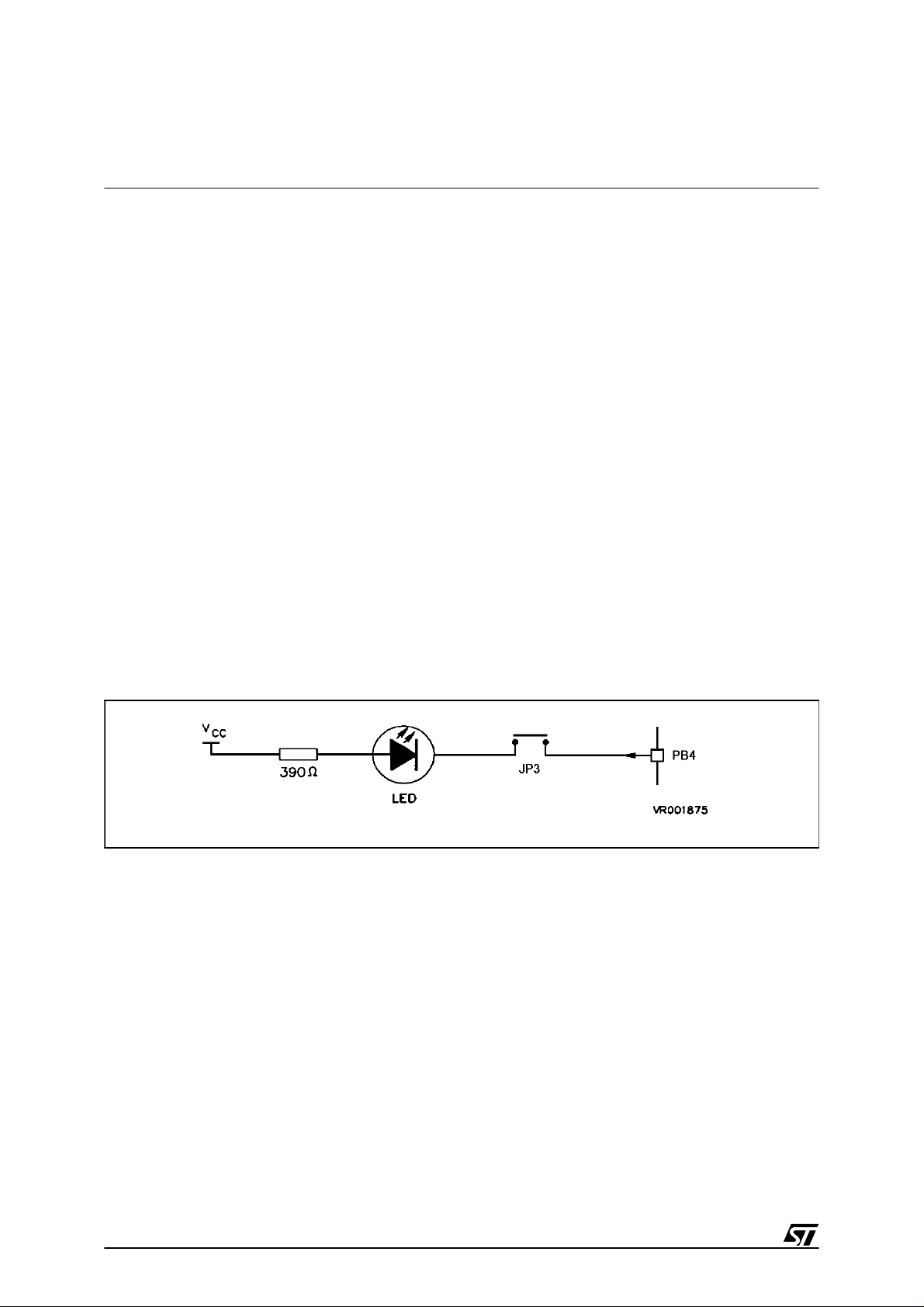
A LED is connected to the ST62T40B PB4 I/O pin (which is defined as output) to demonstrate
the ST6 LED-driving capacity. It can be disconnected from PB4 by removing the jumper JP3.
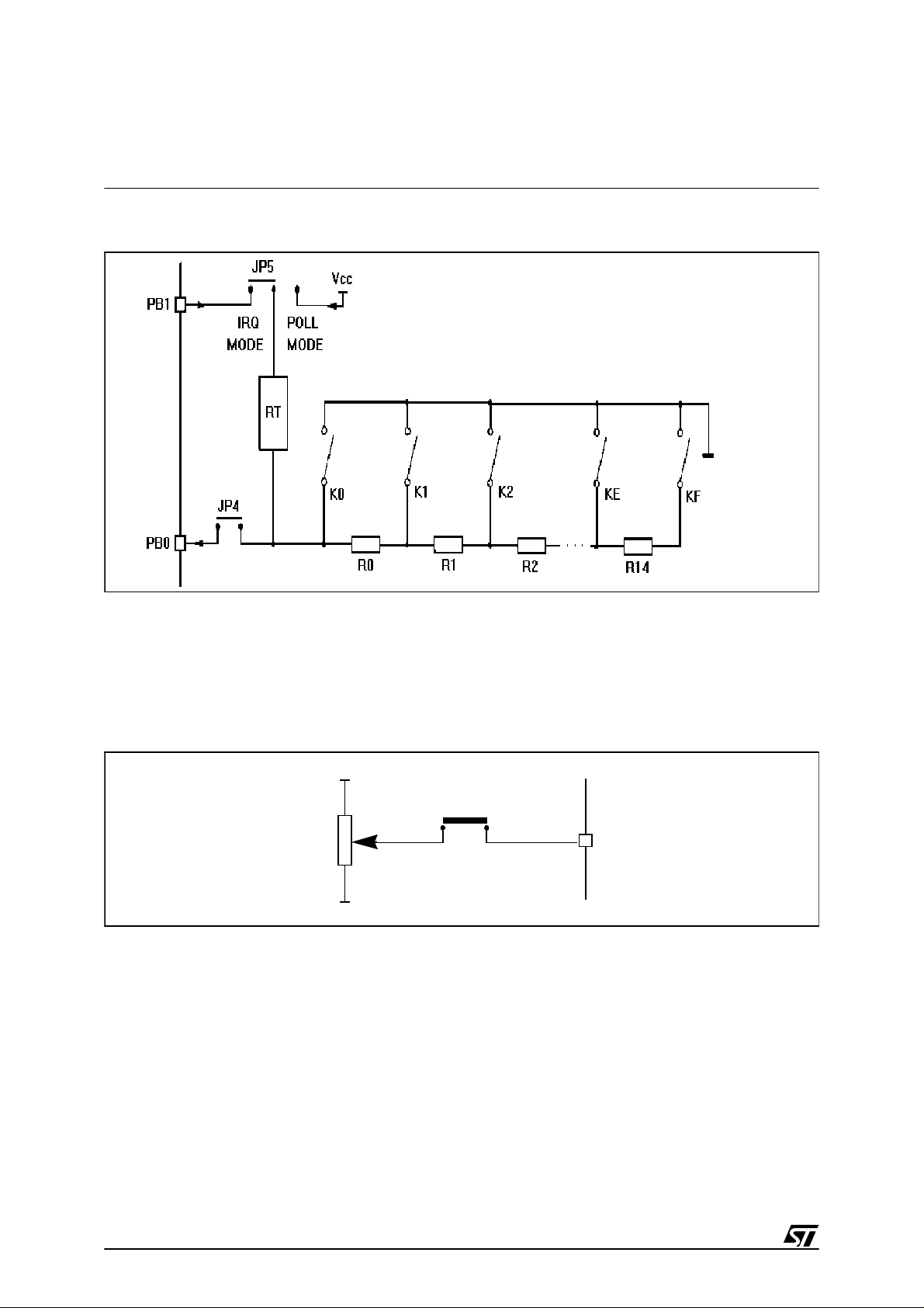
2.7 Hexadecimal Keyboard
A hexadecimal keyboard is connected to the ST62T40B PB0 I/O pin (defined as A/D Converter input), via an analog interface resistor array.
The voltage value on the A/D converter input is equal to 5V/16 x the key number, thus giving
an image of the pressed key.
16
Page 13
13/49
The Starter Kit Hardware
The following table lists the Resistor array values and their corresponding voltage/key values:
Jumper JP5 sets the keyboard operation mode: polling or IRQ, according to the following diagram.
Jumper JP4 disconnects the keyboard output from PB0 when it is removed, enabling you to
connect your own external source to PB0 via the J1 connector.
For an example of the analog keyboard application, refer to the SGS-Thomson application
note AN431: Using ST6 Analog Inputs for Multiple Key decoding.
Resistor Array Values Theoretical Voltage Values
RT: 1K
Ω
NO KEY: 5V
R0: 68
Ω
K0: 0V
R1: 75
Ω
K1: 0.312V
R2: 82
Ω
K2: 0.625V
R3: 100
Ω
K3: 0.937V
R4: 120
Ω
K4: 1.250V
R5: 150
Ω
K5: 1.562V
R6: 180
Ω
K6: 1.875V
R7: 220
Ω
K7: 2.187V
R8: 270
Ω
K8: 2.500V
R9: 390
Ω
K9: 2.812V
R10: 560
Ω
KA: 3.125V
R11: 820
Ω
KB: 3.437V
R12: 1.2K
Ω
KC: 3.750V
R13: 2.7K
Ω
KD: 4.062V
R14: 7.5K
Ω
KE: 4.375V
KF: 4.687V
JP5
This pos it io n
selects polling.
This position
selects IRQ.
JP5
17
Page 14
14/49
The Starter Kit Hardware
Analog Keyboard diagram:
2.8 Resistance trimmer
A 10 KΩ resistance trimmer feeds the ST62T40B PA4 I/O pin (when programmed as an A/D
Converter input) with a variable voltage (0 to 5V DC). It is used for A/D conversion demonstration/evaluation.
The trimmer can be disconnected from the PA4 I/O pin by removing the JP6 jum per.
2.9 Combi-ports PC0-7
The port C of the ST6240B is used for the LCD segments. It can be used as a normal port in
hardware simulation mode.
The port PC0-7 can be accessed on J2, prior to use it, remove the 8 jumpers on JP2 (marked
14 on the Starter Kit board diagram on page 11). Thus, the LC D won’t be aff ected by the inputs on the port PC0-7 and won’t be damaged.
TRIMMER
V
DD
PB4
JP6
JUMPER
ST62T40B
RV1
GND
18
Page 15

15/49
Installing the Starter Kit
3 INSTALLING THE STARTER KIT
3.1 Hardware and Software Requirements
To be able to install and run the ST6 Starter Kit, you need a PC with:
• A 3 1/2” Floppy Disk Drive
• A free Centronics compatible parallel port connector
• MS-Windows
TM
3.11, NT or 95.
• A CD-ROM Disk Drive
3.2 Installing the Software
If diskettes are provided, you must install the software with them in order to have the latest release:
1
Place the SK624XI1 diskette into your floppy disk drive.
2
In Windows Explorer or File Manager, view the contents of the diskette, then double-click
the
Setup
file or icon.
3
Follow the instructions as they appear on screen.
If only the ST62 CDROM is provided, then:
1
Place the ST62 CDROM provided into your CDROM disk drive.
2
In Windows Explorer or File Manager, view the contents of the CDROM, browse to
st62oncd\ftools\sk624Xi1 and double-click the
Setup
file or icon.
3
Follow the instructions as they appear on screen.
3.3 Connecting the Power Supp ly
If you have AC mains supply, connect the Jack plug on the power supply cable provided to the
J3 input socket, then connect the mains plug to a mains source.
If you have DC mains supply, connect the male plug on the power supply cable provi ded to the
J3 input socket, then connect the mains plug to a mains source with the following characteristics:
• Voltage: 16V min./20V max.
• Current: 100 mA min.
To avoid a short circuit, always connect the power input cable to the starter kit board before
connecting it to a mains power supply.
19
Page 16

16/49
Installing the Starter Kit
If you use your own 3.5 mm power supply plug, its polarity must be as follows:
JACK P LUG
-
+
20
Page 17

17/49
Running the Demos
4 RUNNING THE DEMOS
This section describes the demonstration programs that are provided with the Starter Kit and
explains how to run them.
4.1 What the Demos Do
The following paragraphs describe the demos that come pre-loaded with the ST6 Starter Kit
demos. See “Running the Demonstration Programs” on page 18 below for details on how to
select and run a demo.
The source files of these demos are provided with the Starter Kit software in the file
C:\st6tools\sk624Xi1\sk624Xli\DEMOKIT2.ASM.
4.1.1 Demo 1 - Key Display
1
Initialises the pin PB0 (which is connected to the keyboard) as an analog input.
2
Polls the A/D converter to detect whether a key is pressed.
3
When a key is pressed, it shifts the contents of the LCD one place to the left and displays
the value of the pressed key on the right side of the LCD.
To stop the demonstration, press the Reset button. To quit the demonstration routine and bypass the presentation message, press and r elease the Reset button while pressing any key on
the Starter Kit keyboard.
4.1.2 Demo 2 - Voltmeter
1
Initialises the pins as follows:
2
Reads digital value of the voltage present on PA4 from the A/D converter data register.
3
Displays the read voltage value on the LCD panel. When the read value reaches 4 volts,
the LD1 LED is switched on indicating that the voltage value is reaching its upper limit.
You can adjust the voltage value using the voltage trimmer (marked 11 on the Starter Kit
board diagram on page 11).
To stop the demonstration, press the Reset button. To quit the demonstration routine and bypass the presentation message, press and r elease the Reset button while pressing any key on
the Starter Kit keyboard.
The LED flickers when around 4 volts is reached. This is because of the power s upply voltage
noise >20 mV or instability of the resistor trimmer.
This pin: Is initialised as:
PA4 Analog input. Connected to the trimmer RV1.
PB4 20 mA direct LED drive output.
21
Page 18

18/49
Running the Demos
4.2 Running the Demonstration Programs
The ST62T40B microcontroller labelled DEMOKIT2 is programmed with the demonstration
software.
To run the demonstrations:
1
Power down the Starter Kit board.
2
Make sure that the ST62E46B is not plugged into the SDIP56 ZIF MCU socket.
3
Select the USER mode using the jumpers marked JP1 (marked 2 on the Starter Kit board
diagram on page 11), as shown in the diagram below:
4
Disconnect the cable from the parallel port (P2) connection, if it is connected.
5
Power up the Starter Kit board.
6
Press and release the Reset button on the Starter Kit board. When the message “Press key
1\2” is displayed on the LCD, press either 1 to run the Keyboard demonstration or 2 to run
the Voltmeter demo.
To stop the current demonstration and view the other demonstration, repeat s tep 6 above. Or,
to avoid the display of the presentation message, press any key on the Starter Kit keyboard
then, while keeping the key pressed, press and release the Reset button.
USER
PROG
22
Page 19

19/49
Connecting External Resources to the Starter Kit Board
5 CONNECT ING EXTERNAL RESOUR CES TO THE STARTER KIT BOARD
You can connect your own external resources to the pre-programmed ST62T40B to debug or
evaluate your programs, using the connector J1 (marked 17 on the Star ter K it board diagram
on page 11).
You can also connect your own LCD to the ST62T40B LCD driver using the connector J2
(marked 16 on the Starter Kit board diagram on page 11).
To be able to use either of these connectors, y ou must disconnect the resources that are already connected to the ST62T40B, to avoid external resource/Starter Kit board resource conflicts.
The following tables list the Starter Kit board resources and the corresponding J1 and J2 connections, and indicates the jumper that disconnects each resource
Table 1. J1 User’s I/O Interface Connector
NOTE:
1. The 5V supply is available up to 200mA max current.
2. 32KHz oscillator is mounted on PCB at XT1, C5 and C6 locations.
Signal Pin Number Pin Number Signal
5V supply
(1)
125V supply
(1)
RESET 3 4 PSS
OSC32in
(2)
5 6 OSC32out
(2)
PB0
(3)
7 8 PB1
(4)
PB2 9 10 PB3
PB4
(5)
11 12 PB5
PB6 13 14 PB7
TIMER 15 16 NMI
OSCout 17 18 OSCin
WDON 19 20 Unused
Unused 21 22 Unused
Unused 23 24 PA3
PA4
(6)
25 26 PA5
(7)
PA6
(7)
27 28 PA7
(7)
GND 29 30 GND
23
Page 20

20/49
Connecting External Resources to the Starter Kit Board
3. PB0 is connected to Analog Keyboard Array output. It c an be disconnected by removing
jumper JP4.
4. PB1 may be connected to Analog Keyboard reference voltage input (for interrupt mode). It
can be disconnected by removing jumper JP5.
5. PB4 is connected to LED LD1. It can be disconnected by removing jumper JP3.
6. PA4 is connected to the trimmer RV1. It can be disconnected by removing jumper JP6.
7. PA5, PA6, PA7 are used to perform data transfer in programming mode (PROG c onfiguration). In case these signals are connected to external user’s sources, those sources
must be disconnected (or set to High Z state) during programming operations.
PA0, PA1, PA2 are used to perform data transfer with PC simulator software. They are not
available for external usage in this operating mode. Thus, they are not present on J1 connector.
Table 2. J2 User’s LCD Interface Connector
Signal Pin Number Pin Number Signal
Unused 1 2 Unused
Unused 3 4 Unused
S47 5 6 S48
S45 7 8 S46
S43 9 10 S44
S4111 12S42
S39/PC6
(1)
13 14 S40/PC7
(1)
S37PC4
(1)
15 16 S38/PC5
(1)
S35PC2
(1)
17 18 S36/PC3
(1)
S33/PC0
(1)
19 20 S34/PC1
(1)
S3121 22S32
S2923 24S30
S2725 26S28
S2527 28S26
S2329 30S24
S2131 32S22
S1933 34S20
S1735 36S18
S1537 38S16
S1339 40S14
S1141 42S12
24
Page 21

21/49
Connecting External Resources to the Starter Kit Board
NOTE:
1. The combi-port PC0-7 can be accessed on J2. It is normally connected to the LCD pins
but, however, these LCD pins can be disconnected with JP2 jumper in order to use the
combi-port. After Reset, these pins are configured automatically as LCD segment.
2. The VLCD input pin is connected to 5V supply voltage through a jumper between pins 57
and 58. To connect another voltage source, first remove this jumper and then feed pin 58
with the new VLCD voltage.
3. For the Starter Kit LCD, VLCD1/3 and VLCD2/3 are generated by the ST62T40B internal
resistor divider. If needed, an external di vider can be connec ted to these two pi ns as described in ST6240 data book, especially if VLCD < 4.5V.
S9 43 44 S10
S7 45 46 S8
S5 47 48 S6
Unused 49 50 S4
Unused 51 52 Unused
COM2 53 54 COM4
COM1 55 56 COM3
5V
(2)
57 58 VLCD
(2)
VLCD1/3
(3)
59 60 VLCD2/3
(3)
Signal Pin Number Pin Number Signal
25
Page 22

22/49
Using The Starter Kit Board as a Hardware Simulator
6 USING TH E STARTER KIT BOAR D AS A HARDWARE SIMUL AT OR
WGDB6, the ST6 debugger that runs under Windows, lets you test your programs without
having to program the EPROM of your target ST6. Depending how much information you
want, and how close to real life you want your test environment to be, you can use WGDB6 in
one of three ways:
• As a software simulator. If you use WGDB6 as a simulator, you need not attach any additional hardware to your PC. The ST6 simulator program, that comes with WGDB6 and i s
run when you run WGDB6/Simulator, simulates the execution of your program, letting you
step through the code and see what happens as the program runs. WGDB6 simulator
includes Wave Form Editor, which simulates the output of the pins on your target ST6 in
relation to inputs that you define, enabli ng you to see how its peripherals react to the inupts
they receive.
• With an ST6 hardware emulator. Emulators are hardware systems that act as your target
microcontroller, at the same time capturing detailed information, such as which areas of
memory are accessed by the program and what happens when they are accessed. In this
case, WGDB6/Emulator provides an interface between the emulator and your PC, displaying data captured by the emulator and letting you implement the WGDB6 features in the
emulator, such as software or hardware breakpoints.
• With the Starter Kit board as a hardware simulator. This is a cross between the abov e two.
The WGDB6 software simulator simulates the execution of your program, but each time
the data space is accessed, it accesses that of the ST6 that is plugged into your Starter Kit
board. Thus, using the Starter Kit board with WGDB6, you can view how the real microcontroller peripherals behave when your program is executed.
This section describes the third option, how to use the Starter Kit board as a hardware simulator.
You can use the Starter Kit board to emulate any ST624x microcontroller.
When simulating programs designed for other microcontrollers, make sure that you do not use
resources that are not available on the microcontroller your application is designed for.
26
Page 23

23/49
Using The Starter Kit Board as a Hardware Simulator
6.1 The Data Transmission Driver
Data is transferred between the simulated peripheral registers and the ST62T40B registers
via the host PC’s parallel port. The D EMO KIT2.HEX pr ogram, w hich is in the ST62T40B microcontroller that is soldered on the Starter Kit board includes the transmission driver.
The data transfer driver uses the following pins:
Note
: Do not connect any external r esources to the corresponding J1 c onnector pins when us-
ing the Starter Kit board as a peripheral emulator.
6.2 Technical Limitations
The Starter Kit board has the following limitations when used with WGDB6 as a hardware simulator:
• Real-time program execution is not supported. The program execution speed depends on
your PC.
• Resetting the ST62T40B by power up, pressing the Reset button or external reset does
not reset the simulated ST6 core. To perform a complete simulated reset, use the WGDB6
reset command instead.
• Interrupts sent by the ST62T40B microcontroller are not supported by the WGDB6 simulator.
• The pins: NMI, PA0, PA1 and PA2 on the ST62T40B microcontroller are used for communications with the host PC, and are thus not available for simulation.
PC
parallel port
ST62T40B SIMULATOR USAGE
D2 PA2 Synchronisation
D3 PA0 Write data to MCU
D4 RESET Hardware reset of peripherals
D6 NMI Initiates data transfer
SDOP PA1 Read data from MCU
27
Page 24

24/49
Using The Starter Kit Board as a Hardware Simulator
To use the Starter Kit board as a hardware simulator:
1
Power down the Starter Kit board.
2
Make sure that the ST62E46BF1 is not plugged into the SDIP56 ZIF MCU socket.
3
Select the USER mode using the jumper JP1 (marked 2 on the Starter Kit board diagram on
page 11), as shown in the diagram below:
4
Connect the Parallel port P2 on the Starter Kit board to a spare parallel port on your PC using the cable provided with the Starter Kit.
5
Power up the Starter Kit board.
To run WGDB6:
• If you are using Windows 95, click the
Start
button, point to
Programs
, then
ST6 Tools
,
then click
WGDB6/Simulator
.
• If you are using Windows 3.x, double-click the appropriate
WGDB6/Simulator
icon in the
ST6 Tools
program group.
Refer to "WGDB6 User Guide" in the "ST6 Family Software Development Tools AST6, LST6,
WGDB6" User Manual for full instructions on how to use WGDB6.
USER
PROG
28
Page 25

25/49
Using The Starter Kit Board as a Hardware Simulator
6.3 Error Messages
The following table lists the error messages you may encounter when using WGDB6 with the
Starter Kit board:
6.4 Troubleshooting
If there is a communication problem between WGDB6 and the Starter kit board, the title
“WGDB6 Simulator” appears in the WGDB6 title bar. In this case, you shoud check the following:
• That the Starter Kit board is correctly powered up.
• That the parallel port cable is correctly connected.
• That the device jumper JP1 is in the USER position.
• That no ST62E46B is plugged into the Starter Kit board.
Error message Description
Error 116 Port A protected when using board. This means that WGDB6 tried to access the PORT A
registers. These are used for communications with
the board.
Error 117 Communication error with ST624x
board.
This means that a problem occurred during
communications between the host PC and the board.
Perform the checks listed below.
29
Page 26

26/49
Exercises
7 EXERCISES
This section describes two exercises, in whi ch y ou use your ST6 Starter Kit board as a hardware simulator with WGDB6:
• In the first excercise, you’re going to learn how to use WGDB6 to reset the LCD on your
Starter Kit board then display the letter A on it.
• In the second excercise, you’re going to use WGDB6 to step through the instructions that
display messages on the keyboard.
7.1 Exercise 1
1
Connect your Starter Kit board as a Hardware Si m u lator following the instructions given in
“Using The Starter Kit Board as a Hardware Simulator” on page 22.
Press the Reset button on the Starter Kit.
2
Run WGDB6 Simulator:
If you are using Windows 95, c lick the
Start
button, point to
Programs
, then
ST6 Tools
,
then click
WGDB6/Simulator
.
If you are using Windows 3.x, doubl e-click the appropriate
WGDB6/Simulator
icon in th e
ST6 Tools
program group.
The message ‘REMOTE’ is displayed on the LCD of the Starter K it board.
The WGDB6 main window opens:
3
Load the file
Stktrain.hex
:
i
In WGDB6, on the
File
menu, click
Open
.
ii
Browse to the director
y
c:\st6tools\sk624Xi1
iii
Select the file
stktrain.hex
, then click OK.
4
The Disassembler window now opens, displaying the source code of
stktrain.hex
.
30
Page 27

27/49
Exercises
5
Reset the simulated program: on the
Commands
menu, click
Reset
.
The disassembler window opens, displaying the line
0xffe
, which is set by the reset vector.
The LCD panel on the Starter Kit board is now clear, indicating that the WGDB6 simulator
performed a physical reset of the ST62T40B plugged into the starter kit board. When the
reset was performed, all segment outputs were set to OFF by setting the HFE bits 2, 1 and
0 of the LMCR register to 0. The LMCR register sets the LCD control mode. For full details
about the LMCR, see the ST6240 Data Book.
31
Page 28

28/49
Exercises
You are now going to locate the register LMCR, an d change its value:
1
In the WGDB6 main window, on the
Windows
menu, click
Browser
.
The Browser dialog box opens:
2
From the
Type
drop down list, choose data, as shown above (LMCR is a data address).
3
In the
Filter
field, type
LMCR
, as shown above.
4
Click
Apply
.
LMCR
is now displayed in the
Symbols
matching box, as shown above.
5
Select LMCR in the
Symbols matching
box, then click
Inspect
.
The Inspect window opens, displaying the value of LMCR (which is 0):
32
Page 29

29/49
Exercises
You are now going to change the value of LMCR to 36:
1
In the Inspect window, select the value ‘0’, then on the
Edit
menu, click
Modify
, and over-
type the value 0 with 36, and click
Set
. The contents of the inspect window are now
36
‘$’
, indicating that the new LMCR value is 36. The value 36 corresponds to the following
configuration:
bits DS1-0 = hold the values 0 0, defining 1/4 duty.
bits HF2-0 = hold the values 1 1 0, setting %256 main osc.
bits LF2-1 = hold the values 1 1 0, setting the LCD frequency to 512 Hz.
2
Look at the LCD on the Starter Kit board, it now displays the message ‘
REMOTE
’.
(If you already used the program, the message may not be ‘REMOTE’. It depends on what
is in the memory)
You are now going to manually build the character ‘A’ that will be displayed on the LCD:
1
In the
Inspect
window, on the
Edit
menu, click
Dump
. The dump window opens, cl ick on
‘Data’ to display the contents of the data space starting at the address
0d0
.
2
In the
Address
field in the Dump window, type the address
0e0
, then press the Enter key
on your keyboard. This moves the cursor to the beginning of the LC D RAM area. Observe
the values from
0E0
to
0F7
: these correspond to the letters ‘R EMOTE’ that ar e displayed
on the LCD. Overtype all these values with the value ‘00’, by repeatedly pressing the 0 key
on your keyboard: you will note that all LCD panel segments are turned off.
33
Page 30

30/49
Exercises
3
To build the letter A, in the Dump window overtype the values 00 with the following values:
Look at the LCD: the character ‘A’ is now displayed at digit 0. Now try writing some of your own
characters, using the information provided in “LCD Interface” on page 36.
7.2 Exercise 2
1
With
stktrain.hex
still loaded in WGDB6, in the WGDB6 main window, on the
Commands
menu, click
Reset
to reset the program.
The Disassembler window opens, with the l ine
jp init
highlighted: this is the line pointed
to by the reset vector.
2
In the WGDB6 main window, click the
Cont
button. The program counter jumps to the init
address, which is the beginning of the program.
Look at the Starter Kit LCD: it is first cleared, then the word ‘
DISPLAY
’, followed by ‘
KEY
’ is
displayed on it. Press some keys on the starter kit keyboard, and note the result: the keys
you press are displayed on the right side LCD. Bear in mind that the program is being simulated, and thus is not running i n real time mode, so you may have to keep keys pressed for
several seconds until they are displayed on the LCD.
3
In the WGDB6 main window, click the
Stop
button.
4
In the Disassembler window, type
m_disp
in the top right field, next to the
Page
field, and
press the Enter key on your PC keyboard.
The disassembled code around the address
m_disp
is displayed, with the
m_disp
ad-
dress highlighted. Click the
Break
button in the Disassembler window to set a breakpoint
At this address: Which corresponds to this
value:
Type this value:
0e1 COM1 02
0e7 COM2 0e
0ed COM3 07
0f3 COM4 00
34
Page 31

31/49
Exercises
on the
m_disp
address: program execution will now stop when the PC reaches this ad-
dress.
5
In the Disassembler window, on the
Commands
menu, click
Reset
.
6
Type
init
in the top right field, next to the
Page
field, and press the Enter key on your PC
keyboard. The program counter now jumps to the beginning of the program.
7
On the
Commands
menu, click
Conti nue
. This continues running the program, until the
breakpoint you placed on the line of
m_disp
is reached. Wait for program execution to
stop.
8
Click th e
Next
button to execute the next line of the program, and look at the LCD : it dis-
plays one segment, that has been turned on by the instruction:
ldi E1, 80
. Keep press-
ing the
Next
button to execute each instruction in turn, watching the effects each one has
on the LCD. You will notice that each time you press the
Next
button, a few more segments
are turned on, until the word ‘
DISPLAY
’ appears on the LCD.
Now that you are familiar with WGDB6, try stepping through the program yourself, observing
the effects each command has on the LCD, and modifying data to see the effect it has on the
LCD.
35
Page 32

32/49
Programming S T6 Microcontr ol lers
8 PROGRAMMING ST6 MI CROCONTRO LL E RS
You can use the Starter Kit board, in conjunction with the program Epromer, to program
ST62E46B or ST62T46B microcontrollers. You can also perform in-circuit programming of
ST62E4X or ST62T4X OTP/EPROM microcontrollers using your own board, connected to the
Starter Kit board via the c onnector P1 (marked 1 on the Starter Kit board di agram on page 11).
NOTE:
The PA5, PA6, PA7 and RESET pins are used to perform programmi ng operations. If these
pins are connected to an external resource via J1, y ou must either disconnect them (see “Connecting External Resources to the Starter Kit Board” on page 19) or set them to high impedance state during programming operations.
This section describes how to set up the Starter Kit board for programming microcontrollers,
and lists the connection requirements for in-circuit application boards.
8.1 Setting Up the Starter Kit Board
1
Power down the Starter Kit board.
2
Plug the ST62E46B/T46B microcontroller you want to program into the MCU socket on the
Starter Kit board.
3
Select the PROG mode using the jumper JP1(marked 2 on the Starter Ki t board diagram on
page 11), as shown in the diagram below:
USER
PROG
36
Page 33

33/49
Programming ST6 Microcontrollers
4
Connect the Parallel port P2 on the Starter Kit board to a spare parallel port on your PC using the cable provided with the starter kit.
5
Power up the Starter Kit board.
You can now use E promer to progr am the microcontroller that is plugge d into the Starter Kit
board.
NOTE :
Epromer does not work under Windows NT.
To run Epromer from Windows 3.x, double-click the Epromer icon in the ST6 Tools group.
To run Epromer from Windows 95, click
Start, Programs, ST6 Tools
, then
Epromer
.
For instructions on how to operate Epromer, click
Help
in the Epromer main window.
8.2 In-Circuit Programmin g
You can perform in-circuit programming of ST 62E4x and ST62T4x EPROM/OT P microcontrollers using your own board, connected to the Starter Kit board via the connector P1 (marked
1 on the Starter Kit board diagram on page 11).
8.2.1 Application Board Connections
The following paragraphs specify the connection requirements between your application
board and the Starter Kit board.
The application board must have a suitable 16-way connector (8x2 header HE10) to be connected via a 16-way cable to connector P1 ( marked 1 on the Starter Kit board diagram on
page 11) on the Starter Kit board.
The following table shows the required pin connections:
Table 3. Signal interconnectio n to different ST6 families
8x2 Connector I/O S T6 21X /2X ST624X ST626X/9X
Pin 1 O PB6 PA6 PB3
Pin 3 O PB5 PA5 PB0
Pin 5 O OSCin OSCin OSCin
Pin 7 I PB7 PA7 PB2
Pin 9 O RESET RESET RESET
Pin 11 I OSCout OSCout OSCout
Pin 13 O VPP/TM VPP/TM VPP/TM
Pin 14+16 Power VDD VDD VDD
Pin 2+4+8 Power VSS VSS VSS
37
Page 34

34/49
Programming S T6 Microcontr ol lers
V
DD
Use of the
V
DD
connection is optional, depending on whether the application board supply can
or cannot be disconnected. If the application board supply is disconnected, you can supply it
through pins 14 and 16 of the connector, as long as the total load current does not exceed 100
mA, and the capacitive load is less than 50 µF.
If the application board has its own power supply, its voltage must be set to 5V, so that logic
levels are compatible with those of the Starter Kit board.
OSCin
Synchronises the programming operations using a clock generated by the programming tool.
OSCin is located on the application board, and must be directly connected to Pin 5 on the 16way connector. No isolation is needed as long as a quartz crystal or ceramic resonator is used
in the application. If an external clock generator is used in the application, it mus t be disconnected during in-circuit programming.
RESET
Controls the programming mode entry. To prevent signal level contention, RESET must be di rectly connected to Pin 9 on the 16-way connector, and must be isolated from other nodes on
the application board. Any direct connection to V
DD
, V
SS
or an output must b e avoided. This
pin can be connected to a CMOS input, a 2 KΩ pull-up, a 10 KOhm pull-down or left open (Internal pull-up). The capacitive load of the RESET pin should not exceed 1
µ
F.
Pins 1 and 7
on the 16-way connector are used to establish communications between the
programming tool and the microcontroller.
To prevent signal-level contention, Pins 1 and 7 must be directly connected to PA6 and PA7
on the 16-way connector, and must be isolated from other nodes on the application board. Any
direct connection to V
DD
, V
SS
or an output must be avoided. These pins may be connected to
a CMOS input, a 2 KΩ pull-up, a 10 KOhm pull-down or left open (Internal pull-up).
If
pin 3
on the 16-pin connector is connected to the target device, the same applies. Connec-
tion to pin 3 is not necessary if a high voltage level is guaranteed by the board design.
Some
I/O pins
are not connected to the 16-way connector and must be set to a high level during programming. This is normally achieved by the RESET signal sent by the programming
tool through the 16-way cable, setting the I/O pins as inputs with an internal 300 KΩ pull-up.
To keep these I/O lines high, direct connection of these pins to GND or to any other signal at
low level (even temporarily) must be avoided. Only connections to another CMOS input, to an
external pull-up or a 10 MΩ pull-down is allowed.
The
Vpp/TM
pin must not be directly connected to GND/V
SS
on the application board, to avoid
any conflict with the programming voltage provided by the programming tool via pin 13 on the
38
Page 35

35/49
Programming ST6 Microcontrollers
connector. This pin should be pulled down by a resistor with minimum value of 10 KΩ. You must
add a 100 nF ceramic capacitor between Vpp/Test and V
SS.
8.3 Setting Up the Starter Kit Board for In-Circu it Programming
1
Power down the Starter Kit board.
2
Select the PROG mode using the jumpers JP1 (marked 2 on the Starter Kit board diagram
on page 11), as shown in the diagram below:
3
Connect the Parallel port P2 on the Starter Kit board to a spare parallel port on your PC using the cable provided with the starter kit.
4
Connect your application board to the connector P1 (marked 1 on the Starter Kit board diagram on page 11) on the Starter Kit board.
5
Power up your Starter Kit board.
You can now use Epromer to program the microcontroller that is on your own board.
NOTE:
Epromer does not work under Windows NT.
To run Epromer from Windows 3.x, double-click the Epromer icon in the ST6 Tools group.
To run Epromer from Windows 95, click
Start, Programs, ST6 Tools
, then
Epromer
.
For instructions on how to operate Epromer, click
Help
in the Epromer main window.
If your application board is not powered by the Starter Kit, you must connect it to a 5V DC power supply before you start programming.
PROG
39
Page 36

36/49
LCD Interface
9 LCD INTERFACE
9.1 ST6240 LCD DRIVER OVERVIEW
This is a quick summary of the features of the ST6240 LCD driver. Refer to the ST6240 data
book for more detailed information.
The ST6240 LCD driver comprises LCD control logic, a programmable prescaler, a 24-byte
wide dedicated LCD RAM, 45 segments and 4 c ommon outputs. This drives up to 180 LCD
segments.
The LCD control logic operates automatically and without interrupting the processor.
The LCD driver configuration is defined by the following ST6240 registers:
• LMCR (LCD Mode Control Register), which defines the LCD backplanes (duty cycle) and
the frame frequencies used by the LCD.
• LCD RAM (24 bytes), which sets each segment to O N or OFF by setting or resetting the
corresponding bit. According to the contents of the LCD RAM, the drivers generate the
segments and common signals which can directly drive an LCD panel.
Hardware configuration requirements are reduced to minimum:
• The VLCD input pin must be fed with VLCD voltage (independently of VMVDD), according
to your LCD panel specifications.
• The VLCD1/3, VLCD2/3 pins are connected to interm ediate VLCD voltages, to enable
external capacitive buffering or resistive shunting. An internal resistor network is implemented so that in most cases, thus no additional components are necessary.
To interface with the LCD panel, all you have to do is:
• Determine the operating LMCR register value according to the LCD panel specifications.
• Generate the correct VLCD v oltage and, i f needed, connect an external resistor network to
the VLCD1/3 and VLCD2/3 pins.
• Determine the most suitable mapping between the LCD panel segments and the LCD
RAM bits.
Once you’ve completed the above s teps, c ontrolling the LCD panel becomes as easy as modifying software bits.
40
Page 37

37/49
LCD Interface
9.2 STARTER KIT LCD PANEL INTERFACE
The following paragraphs describe how the starter kit LCD panel interfaces with the
ST62T40B microcontroller.
The LCD panel used on ST62T40B Starter Kit board has 8 alphanumeric digits.
Each digit is based on a 16-segment m atrix operating in mul tiplexed mode (1/4 duty) so that
only 4 segment pins are required per digit.
Thus the following pins are required for the 8 digits:
• 32 segment (SEG) pins
• 4 common (COM) pins
VLCD operating mode is 5V.
Digits are annotated from 0 to 7 respectively from right to left as s hown by th e fol lowing dia-
gram:
X
B
D
F
E
C
GK
LN
H
J
DP
I
M
VR0A1879
E
D
M
G
L
C
DP
N
K
H
F
I
A
B
J
E
D
M
G
L
E
C
DP
N
K
D
M
L
GNK
X
H
F
I
A
BJF
X
H
I
J
A
C
DP
B
digit digit
digit digit
7
6
54
digit
D
digit
3
DP
E
X
F
NL
M
GK
L
C
E
G
A
H
J
I
X
BF
H
DDD
2
DP
digit
1
DP
0
digit
DP
N
M
C
E
K
NL
M
GK
X
J
I
A
BF
H
J
I
A
L
C
E
G
N
M
C
K
X
BF
H
J
I
A
B
A
X
8 ALPHANUMERIC DIGI TS LCD
41
Page 38

38/49
LCD Interface
Each digit is made up of 16 segments (A,B,C,D and so on) as shown by the following diagram:
Each segment can be set to ON or OFF, depending on the state of its dedicated Segment and
Common lines, according to the boolean equation:
segment ON = Seg_line and Com_line active
Each DIGIT requires 4 SEG lines X 4 COM lines to be completely defined. The following diagram shows the graphic segments that are switched on according to each active COM:
X
A
B
D
F
E
C
GK
LN
H
J
DP
I
M
VR001879
X
A
B
D
F
E
C
GK
LN
H
J
DP
I
M
VR0B1879
E
D
M
G
L
C
DP
N
K
X
H
F
I
A
B
J
E
D
M
G
L
E
C
DP
N
K
D
M
L
G
N
K
X
H
F
I
A
B
J
F
X
H
I
J
A
C
DP
B
COM1 COM2 COM3 COM4
42
Page 39

39/49
LCD Interface
The following table shows the mapping between graphic elements set and the segment/common pins.
Table 4. Digit Matrix to Segment/COM Pins Mapping
For example, the graphic element 7J (J of digit 7) is driven by SEG l ine S2 (pin 2) and COM
line C2 (pin 19). For digit 2, pin 12 drives segments I,J,K,N when COM lines C1,C2,C3,C4 respectively are active.
PIN SEGMENTS PIN SEGMENTS PIN SEGMENTS
1
7X
7F 7E 7D 13 1X 1F 1E 1D 25 2A 2B 2C 2DP
27I7J7K7N141I1J1K1N262H2G2L2M
36X6F6E6D150X0F0E0D273A3B3C3DP
46I6J6K6N160I0J0K0N283H3G3L3M
5 5X5F5E5D 17 . . . C04 29 4A4B4C4DP
65I5J5K5N18 . .C03. 304H4G4L4M
7 4X4F4E4D 19 . C02 . . 31 5A5B5C5DP
8 4I 4J 4K 4N 20 C01 . . . 32 5H 5G 5L 5M
9 3X 3F 3E 3D 21 0A 0B 0C 0DP 33 6A 6B 6C 6DP
10 3I 3J 3K 3N 22 0H 0G 0L 0M 34 6H 6G 6L 6M
11 2X 2F 2E 2D 23 1A 1B 1C 1DP 35 7A 7B 7C 7DP
12 2I 2J 2K 2N 24 1H 1G 1L 1M 36 7H 7G 7L 7M
COM C1 C2 C3 C4 COM C1 C2 C3 C4 COM C1 C2 C3 C4
43
Page 40

40/49
LCD Interface
9.3 Interfacing The LCD Panel with the ST6240 LCD Driver
When assigning the LCD panel segments to the LCD RAM bits, the mapping used will depend
on the LCD you are using. It is recommended that you define the character mapping after defining your software architecture. Make sure, however that this mapping is kept as si mple as
possible. For example, the description map of each character in LCD RAM should be the
same for all the 8 digits on the LCD.
The LCD panel requires 32 segment lines multiplexed through 4 common lines. This is less
than the capabilities of the ST6240. Segments S9 to S39 and outputs COM1,2,3,4 of ST6240
LCD driver are connected to the LCD panel inputs as described in the following diagram.
VR001880
digit 6
digit 5
digit 4
digit 3
digit 2
digit 1
digit 0
digit 7
COM4
COM3
COM1
COM2
36
35
S40
S38
1
2
S39
S37
ST6240
OUTPUTS
S33
S35
3
4
S36
S34
33
34
S29
S31
5
6
S32
S30
31
32
S25
S27
7
8
S28
S26
29
30
S21
S23
9
10
S24
S22
27
28
S17
S19
11
12
S20
S18
25
26
S13
S15
13
14
S16
S14
23
24
S9
S11
15
16
S12
S10
21
22
COM4
COM3
COM1
COM2
ST6240
OUTPUTS
LCD PANEL
20
19
17
18
44
Page 41

41/49
LCD Interface
The following table lists the location of each digit definition in the ST6 RAM. Note that the
memory is not entirely used.
Table 5. Digit Locations in LCD RAM
Each digit is represented by 4 bits (MSB for odd digits, LSB for even digits) in each COM
memory area. Each set of 4 bits x 4 COMs are assigned to the 16 bits defined above as shown
in the following table.
Table 6. LCD RAM Bits Mapping
LCD RAM Address D7 D6 D5 D4 D3 D2 D1 D0
COM1
E1h Digit 1 Digit 0
E2h Digit 3 Digit 2
E3h Digit 5 Digit 4
E4h Digit 7 Digit 6
COM2
E7h Digit 1 Digit 0
E8h Digit 3 Digit 2
E9h Digit 5 Digit 4
EAh Digit 7 Digit 6
COM3
EDh Digit 1 Digit 0
EEh Digit 3 Digit 2
EFh D ig it 5 Digit 4
F0h Digit 7 Digit 6
COM4
F3h Digit 1 Digit 0
F4h Digit 3 Digit 2
F5h Digit 5 Digit 4
F6h Digit 7 Digit 6
Bit 7/3 Bit 6/2 Bit 5/1 Bit 4/0
COM1 H X A I
COM2 G F B J
COM3 L E C K
COM4 M D DP N
45
Page 42

42/49
LCD Interface
9.4 Character Definition Examples
The following examples show the defi nition of character s using the previously des cribed method.
9.4.1 Character A Definition
The following diagram represents the ‘A’ character to be displayed on the LCD panel.
The following table gives the corresponding bit pattern to be set in the LCD RAM to display the
character ‘A’ on the LCD panel. The bits set to 0 are left blank, and the bits set to 1 are shaded.
The right column provides the corresponding hexadecimal value.
This description is valid for all characters. The position of the displayed character depends
only on the addresses and the position (LS/MS nibble).
D3 D2 D1 D0
Hex
value
COM1
HX
AI2
COM2
G F BJE
COM3
L
E C K7
COM4
MDDPN0
X
A
B
D
F
E
C
GK
LN
H
J
DP
I
M
VR0C1879
46
Page 43

43/49
LCD Interface
9.4.2 Character 3 Definition
The following diagram shows the character 3 to be displayed on the LCD.
The following table gives the corresponding bit pattern to be set in the LCD RAM to display the
character ‘3’ on the LCD panel.
The set of 4 x 4 bits (representing the character set) can be stored in the ST624x DATA ROM
and easily used by display software through indexed accesses.
D3 D2 D1 D0
Hex
value
COM1
H X A I2
COM2
G F B JA
COM3
L E C K3
COM4
M D DP N4
X
A
B
D
F
E
C
GK
LN
H
J
DP
I
M
VR0D1879
47
Page 44

44/49
LCD Interface
9.5 Starter Kit LCD Panel Character Set Software Model
As described in the previous paragraphs, LCD connection and character mapping drive a software model of the LCD-displayable objects. These objects are available for DISPLAY routines
to drive LCD panel display during program execution.
The following paragraphs describe three methods of displaying characters on the LCD.
9.5.1 Direct Code LCD RAM Patching
This is the most simple way to display digits on an LCD. The mapped character values are directly patched into the corresponding LCD RAM locations. The bit map values are contained
in the immediate values of write instructions.
This method should only be used for very simple applications (few characters, displayed few
times) or for rapid evaluation.
The following block of code shows how to use direct code LCD RAM patching to display the
character ‘A’ at digit 0, where x is the value of the MSB (digit 1):
disp_A_0 ldi E1, x2 ;value 2 to digit 0 COM1 addr (E1, LSB)
ldi E7, xE ;value E to digit 0 COM2 addr (E7, LSB)
ldi ED, x7 ;value 7 to digit 0 COM3 addr (ED, LSB)
ldi F3, x0 ;value 0 to digit 0 COM4 addr (F3, LSB)
9.5.2 Indexed Data ROM
The mapped values of character sets are defined into ST6240 Data ROM area (refer to
ST6240 databook). The AST6/LST6
.byte
directive and .w and .d labels define and access
the Data ROM area.
A generic display call subroutine accesses the character definition map through the parameter
passed by the calling program. The
disp_0
subroutine (see below) displays a character at
digit 0 and clears digit 1 (MSB of the same LCD RAM locations).
An efficient generic display subroutine should manage the digit number (as input par ameter)
and perform the read/modify/write only on the concerned nibble in the LCD RAM byte (MSB or
LSB). This is done by the display subroutine delivered with the ST6240 Starter Kit library
(please read the README file provided in the SK6240LIB directory).
A character is defined by 4 x 4 bit words = 16 bits. To optimize the character set size in Data
ROM, it is useful to compact these 16 bits into 2 bytes, however this method increases the display routine complexity.
48
Page 45

45/49
LCD Interface
For the ST6240 Starter Kit demo routines, the character set is defined as follows (for example
character A):
CHAR_A. .byte 22
.byte EE
.byte 77
.byte 00
The character is displayed using the following routine:
disp_A_0 ldi RWSR, CHAR_A.w;set Data ROM Window register
ldi X, CHAR_A.d ;X set to point to CHA R_A
call disp_0 ;subroutine that displays digit 0
disp_0 ld E1, (X) ; output value 2 to digit 0 COM1
;(E1, LSB)
inc X ;X set to second byte of CHAR_A
ld E7, (X) ;output value E to digit 0 COM2
;(E7, LSB)
inc X ;X set to third byte of CHAR_A
ld ED, (X) ;output value 7 to digit 0 COM3
;(ED, LSB)
inc X ;X set to fourth byte of CHAR_A
ld F3, (X) ;output value 0 to digit 0 COM4
;(F3, LSB)
Four bytes are used to define a character, with MSB and LSB equal to the 4 bit definition values. In this way, MSB and LSB are easily distinguished using the AND instruction for masking
the non-relevant nibble.
9.5.3 Complete Message Display
You can simplify the definition of complete messages using the AST6 .ASCIZ directive. This
directive returns the ASCII code pattern of the characters indicated ended by NULL). To enable you to use the .ASCIZ directive, the ST6240 character set is pre-defined in the Data ROM
so that it becomes simple to access a mapped character definition through the character’s ASCII code.
One Data ROM window contains 64 bytes. As a character definition map requires 4 bytes, 16
characters can be defined in a whole window. This corresponds to a page of ASCII codes
(represented by the MSB of the ASCII code).
49
Page 46

46/49
LCD Interface
For example characters @, A, B through O, whose ASCII codes are 40,41,42 through 4F
(Hex) respectively, represent the ASCII code page 4, and fill a Data ROM window as shown
below:
.ORG x00;beginning of a wind ow
0 CHAR_@.byte 22;address 0 in the window
.byte AA
.byte BB
.byte 44
1 CHAR_A.byte 22;address 3 in the window
.byte EE
.byte 77
.byte 00
through
F CHAR_O.byte 22;address 3 C in the window
.byte 66
.byte 66
.byte 44;last address (3F) i n the window
For example, the ASCII code of character A is 41 (hex):
• 4 specifies the Data ROM window number
• 1 indexes the number of the character in the Data ROM window
The available LCD character set that is delivered with the ST6240 Starter Kit library is defined
using this method. This allows the
asci_dis
subroutine to display a character defined by its
ASCII code and
Mdis_mes
subroutine to display a complete message, built using the ASCIZ
AST6 directive, on the LCD panel.
Refer to the files SK6240LI.INI and SK6240LI.ASM in the SK624XLI directory for a description
of these subroutines.
50
Page 47

47/49
Hardware Information
10 HARDWARE INFORMATION
10.1 Part List
10.2 Starter Kit Board Schematic
See next page
Part Device Part Device
U1 74LS244 R1, R16 100
Ω
U2 8M Hz os cillator R2, R11, R28 1K
Ω
U3 S T 62T40 B MCU R3 47
Ω
U4 ST 62E 46B MCU socket R4, R26 39 0
Ω
U5 74LS04 R5, R8 10K
Ω
U6 LCD panel R6 Not connected
U7, U8 78L05 Voltage Regulator R7, R9 4.7K
Ω
U9 7805 Voltage Regulator R10, R27 560
Ω
U10 Keyboard R12 68
Ω
XT1 32.768 KHz crystal R13 75
Ω
RV1 10KΩ resistor trimmer R14 82
Ω
D1, D2, D3 1N4148 diode R15 7.5K
Ω
D4 BYV 10-20 Schottky R17 120
Ω
D5 1N4004 diode R18 150
Ω
Z1 8.2V Zener diode R19 2.7K
Ω
LD1, LD2 Red LED R20 3.3
Ω
T1, T3 BC547B transistor R21 180
Ω
T2 BC557B transistor R22 220
Ω
T4 BD236 transistor R23 270
Ω
L1 Sel f 2x2µH R24, R25 1.2K
Ω
C1, C2, C10, C15 100nF (Cd) R29 820
Ω
C16,C17,C18,C20,C23,C25 100nF RS1, RS5 3.3KΩ SIL8 Array
C3, C4, C7, C8, C9, C11, 100pF RS2 10 KΩ SIL9 Array
C12, C13, C14 100pF RS3, RS4 150Ω SIL8 Array
C5, C6 15pF RV1 10KΩ resistor trimmer
C19, C21 1.0nF P1 Header 2x8
C22 22µF P2 SUBD25-M Connector
C24 10µF J1 2x15 pins connector
C26 1µF J2 2x30 pins connector
SW1 Push-button J3 Female Jack plug
JP1 to JP6 jumpers J4 2nd power supply conn.
51
Page 48

48/49
Hardware Information
TO- 220
TO-92
USER'S I/O INTERFA C E
I N SI TU PROG. CONNECTOR
( enabl es VDD)
(disables RESET/)
( d i sab l es VPP)
PROG
IRQ POLL
USER
Not used
USER' S LCD INTERFACE
SDI P5 6
SOCKET
(SDOP 46B)
LCD Pi ns Prot ect i on i f
Combi -Port PC0- 7 i s used
14 femal e j umpers 2.54
(SDOP 40B)
TO-92
ENVPP Lev el c ompat ibi l i t y
ENVPP Lev el c ompat ibi l i t y
Reset Push
PC i nt erf ace connect or
Parallel Port
Solder Bri dge
Solder Bri dge
Solder Bri dge
Solder Bri dge
Solder Bri dge
Sol der Bri dge
Solder Bri dge
D0
S6
VPP
PA7/SDOP
PB3
OSCP
S22
S25
COM2
S8
OSCOUT
S10
COM1
D1
S21
S15
S44
PPINT
S26
S27
PB3
PA5/TM 2
S14
OSC32O
PA7/SDOP
PA7/SDO P
D2
S7
PB0
SDOP
S16
OSC32I
S18
PB4
PB0
PA6/TR O
PA1
PROG/
TROMIN
VLCD2/3
TM2
D0
D3
S19
PB2
PB7
S23
OSCIN
S24
D4
PB2
PB5
TROMIN
TIMER
VLCD1/3
SIM/
D6
PB4
RESET/
S20
D7
D4
OSCPI
PA5/TM2
S47
PA3
PSS
S5
PA4
OSC32I
PA7/SDOP
REM/
S12
PB6
PA4
VLCD
OSC32I
PB1
S17
RESETP/
RESETP
OSCPI
SDOP
TROMIN
AKEY
OSCPI
S11
PA0
WDON
S13
PA6/TRO
S42
PSS
RESETP/
OSCOUT
PB1
S48
TM2
PA3
S43
D5
PA5/TM 2
PA2
COM3
S45
COM4
REM/
PA0
PA6/TR O
S46
TIMER
PPINT
D1
OSC32O
PB5
ENVPP
SDOP
PA1
COM3
S6S5
S12
S17
S21
S24S23
S29
PC5/S38
S8
S32
PC1/S34
S43
S45
PC2/S35
S9
S25
S46
S47
VLCD2/3VLCD1/3
S13
S20
S22
VLCD
COM1
S15
S18
PC2/S35
PC5/S38
PC3/S36
S30
S31
PC6/S39
PC4/S37
VDD
S26
PC6/S39
S42
S14
S41
PC7/S40
COM2
S10
S16
S19
PC3/S36
PC7/S40
S44
S7
S11
S27
S41
PC4/S37
COM4
S28
S48
PC1/S34S4PC0/S33
PC0/S33
NMI
NMI
PA2
PC0/S33
PC1/S34
PC2/S35
PC3/S36
PC4/S37
PC5/S38
PC6/S39
PC7/S40
S33
S34
S35
S37
S36
S38
S39
S40
S9
S4
PB7
PB6
ENVDD
WDON
OSC32O
OSCP
VPP6240
OSCIN
RESET/
RESET/
PA7/SDOP
PA6/TR O
OSCIN46B
VPP
VPP
PA5/TM 2
PA5/TM2
VDD
OSCIN46B
PA6/TRO
S28
S30
S36
S29
S24
S19
S21
COM3
S37
S31
S40
S34
S18
S10
COM2
S15
S35
S28
S23
S14
S32
S27
S11
S39
S22
S30
COM4
S9
S16
S13
S17
S20
S32
S12
S26
S33
S25
COM1
S29
S31
S38
GND
GND
GND
GND
GND
GND
GND
GND
GND
GND
GND
GND
VCC
VCC
GND GND
GND GND
GND
GND
GND
GND
GND
GND
GND
VCC
GND
GND GND
GND
VDD
VDD
VDD
VDD
GND GND
VDD
VDDVDD
VDD
VDD
VDD
VDD
VDD
GND
VCC
VDD
GND
GND
GND
GND
GND
GND
GND
GND
VDD
U4
ST6246B
PC3/S361PC4/S372PC5/S383PC6/S394PC7/S405S416S427S438COM49COM310COM211COM112VLCD1/313VLCD2/3
14
VSS22VDD21TEST/Vpp20Ain/PA419Ain/PA518Ain/PA617Ain/PA716VLCD
15
RESET23OSCout24PB6/Sin28PB7/Sout27NMI26OSCin
25
PB5/Scl
29
PB4
30
S1342S1241S1140S10
39S938
PSS
37
OSC32in
36
OSC32out
35
PB0/Ain34PB1/Ain33PB2/Ain32PB3/Ain
31
S1443S1544S1645S2546S2647S2748S2849S2950S3051S3152S32
53
PC0/S3354PC1/S3455PC2/S35
56
SW1
5 4
21
3
P2
SUBD25C-F-COUDE
13251224112310229218207196185174163152141
U3
ST62T40B
PB0/Ai n
38
PB1/Ai n
37
PB2/Ai n
36
PB3/Ai n
35
PB4
34
PB5/Scl
33
PB6/Sin
32
PB7/Sout
31
TIMER
30
PA0/Ain22PA1/Ain21PA2/Ain20PA3/Ain19PA4/Ain17PA5/Ain16PA6/Ain15PA7/Ain14COM110COM29COM38COM47S486S475S464S453S442S43
1
S26
64
S42
80
S25
63
S41
79
S24
62
PC7/S4 0
78
S23
61
PC6/S3 9
77
S22
60
PC5/S3 8
76
S21
59
PC4/S3 7
75
S20
58
PC3/S3 6
74
S19
57
PC2/S35
73
S18
56
PC1/S3 4
72
S17
55
PC0/S3 3
71
S16
54
S32
70
S15
53
S31
69
S14
52
S30
68
S13
51
S29
67
S12
50
S28
66
S11
49
S27
65
S10
48S947S846S745S644S543S442
PSS
41
OSC32in
40
OSC32out
39
NMI
29
WDON
28
OSCIN
27
OSCOUT
26
RS
25
VSS24VDD
23
VPP/TM
18
VLCD13VLCD2/312VLCD1/3
11
L1
SELF 2x2.2ÿH
2
43
1
JP2
MW2X8C
1 2
3 4
5 6
7 8
9 10
11 12
13 14
15 16
J2
MW2X30 C
1 2
3 4
5 6
7 8
9 10
11 12
13 14
15 16
17 18
19 20
21 22
23 24
25 26
27 28
29 30
31 32
33 34
35 36
37 38
39 40
41 42
43 44
45 46
47 48
49 50
51 52
53 54
55 56
57 58
59 60
JP6
MW2X1C
1 2
JP4
MW2X1C
1 2
JP3
MW2X1C
1 2
J1
MW2X15C
1 2
3 4
5 6
7 8
9 10
11 12
13 14
15 16
17 18
19 20
21 22
23 24
25 26
27 28
29 30
JP5
MW1X3C
1
2
3
JP1
MW1X3C
123
TP1
MW1X1C
TP2
MW1X1C
I
GND
O
U9
LM7805
1
2
3
LD2
LED-RED-5 MM
12
LD1
LED-RED-5MM
1 2
U6
LCD VIM878
D8.C1D8.A2D7.C3D7.A4D6.C5D6.A6D5.C7D5.A8D4.C9D4.A10D3.C11D3.A12D2.C13D2.A14D1.C15D1.A16COM417COM3
18
D8.D
36
D8.B
35
D7.D
34
D7.B
33
D6.D
32
D6.B
31
D5.D
30
D5.B
29
D4.D
28
D4.B
27
D3.D
26
D3.B
25
D2.D
24
D2.B
23
D1.D
22
D1.B
21
COM120COM2
19
J3
JACK
231
P1
HE10-16DM
1 2
3 4
5 6
7 8
9 10
11 12
13 14
15 16
G8
12
G7
12
G5
12
G3
12
G9
12
G6
12
G1
12
G4
12
F1 EMC_F
1
1
2
2
3
3
J4
ED102
112
2
Z1
DZ 8.2V
1 2
U10
KEYBOARD
K014K11K22K33K45K56K67K79K810K911KA13KB15KC16KD12KE8KF4COM
17
D4
BYV 10-20 SCHO
12
T4
BD236-PNP-60 V
3
1 2
T2
BC557B-PNP-45V
2
1 3
T1
BC547B-NPN-45V
2
1 3
T3
BC547B-NPN-45V
2
1 3
U2
8MHZ-OSC
FOUT
3
R29
820
1 2
R14
82
1 2
I
GND
O
U8
78L05
1
2
3
I
GND
O
U7
78L05
1
2
3
R13
75
1 2
U1
74LS244
1A121A241A361A482A1112A2132A3152A4171G12G
19
1Y1181Y2161Y3141Y4122Y192Y272Y352Y4
3
VDD
20
GND
10
U5E
74LS04
11 10
U5D
74LS04
9 8
U5B
74LS04
3 4
U5F
74LS04
13 12
U5A
74LS04
1 2
U5C
74LS04
5 6
R15
7.5K
1 2
R12
68
1 2
R27
560
1 2
R10 560
1 2
R3
47
1 2
R9
4.7K
12
R7
4.7K
12
R6
4.7K
1 2
R26
390
1 2
R4
390
12
XT1
32.768KHZ-XT-P
1 2
R20
3.3
1 2
R23
270
1 2
+
C22
22MF-EA-25V
12
R22
220
1 2
R19
2.7K
1 2
D3
1N4148
1 2
D2
1N4148
1 2
D1
1N4148
12
D5
1N4004
1 2
+
C26 1MF-ER-63V
12
R11
1K
12
R28
1K
12
R2
1K
12
R21
180
1 2
C6
15PF
12
C5
15PF
12
RS3
150-SIL8-4R-B
2
6
135
7
4
8
RS4
150-SIL8-4R-B
2
6
135
7
4
8
R18
150
1 2
R17
120
1 2
+
C24
10MF-CT-16V
12
RS2
10K-SIL9-8R-B
2 1
3
4
5
6
7
8
9
RV1
10K-RV
3 1
2
R5
10K
1 2
R8
10K
1 2
C13
100PF
12
C9
100PF
12
C12
100PF
12
C7
100PF
12
C8
100PF
12
C3
100PF
12
C4
100PF
12
C11
100PF
12
C14
100PF
12
C16
100NF
12
C20
100NF
12
C23
100NF
12
C25
100NF
12
C10
100NF
12
C2
100NF
12
C15
100NF
12
C1
100NF
12
C18
100NF
12
C17
100NF
12
R16
100
1 2
R1
100
1 2
R25
1.2K
1 2
R24
1.2K
12
C19
1.0NF
12
C21
1.0NF
12
RS5
3.3K-SIL8-4R-B
2
6
135
7
4
8
RS1
3.3K-SIL8-4R-B
2
6
135
7
4
8
G2
12
52
Page 49

49/49
Hardware Information
Notes
:
Information furnishe d i s believed to be accurate an d reliable. H owever, SGS-T HOMSON Microelectro ni cs assumes no re sponsibilit y for the
consequences of use of such information nor for any infringement of patents or other rights of third parties which may result from its use. No
license is granted by implication or otherwise under any patent or patent rights of SGS-THOMSON Microelectronics. Specifications
mentioned i n this public ation are subje ct to change wi thout notice . This publica tion supersede s and replac es all informat ion previously
supplied. SGS-THO MSON Mi croelec troni cs produc ts are not authori zed for u se as crit ical comp onents in life sup port dev ices or sy stem s
without the express wri t ten approval o f SGS -THOMSO N M i croelectr oni cs.
1998 SGS-THOMSON Microelectronics - All ri ghts reserved.
Prin t e d in France by Imprim erie AGL
Purchase of I
2
C Components by SGS-THOMSON Microelectronics conveys a license under the Philips I2C Patent. Rights to use these
components in an I
2
C system is granted provided that the system confor m s t o the I2C Standard Specification as defined by Philips.
SGS-THOMSON Microelectronics Group of Companies
Australia - Brazil - Canada - China - France - Germany - Italy - Japan - Korea - Malaysia - Malta - Morocco - The Netherlands -
Singapor e Spain - Sweden - Sw i tzerland - Tai wan - Thailand - United K in gdom - U.S.A.
5
 Loading...