

SG2525A
®
REGULATING PULSE WIDTH MODULATORS
.
8 TO 35 V OPERATION
.
5.1 V REFERENCE TRIMMED TO ± 1 %
.
100 Hz TO 5 00 K Hz O S C IL LA TO R RA NGE
.
SEPARATE OSCILLATOR SYNC TERMINAL
.
ADJUSTABLE DEADTIME CONTROL
.
INTERNAL SOFT-START
.
PULSE-BY-PULSE SHUTDOWN
.
INPUT UNDERVOLTAGE LOCKOUT WITH
HYSTERESIS
.
LATCHING PWM TO PREVENT MULTIPLE
PULSES
.
DUAL SOURCE/SINK OUTPUT DRIVERS
DESCRIPTION
The SG3525 A s eries of puls e width m odulat or i ntegrated circuits are designed to offer improved performance and lowered external parts count when
used in design ing all types of swi tching power su pplies. The on- chip + 5.1 V refer ence i s trimm ed to
1 % and the input common-m ode range of the er ror
amplifier includes the reference voltage eliminating
external resistors. A sync input to the oscillator allows multiple units to b e slaved or a single u nit to be
synchronized to an external system clock. A single
resistor betw een the C
provide a wide range of dead time ad- justment.
These device s also feature built-in soft-start circuit ry
with only an external timing capacitor required. A
shutdown termin al co ntrols both t he s oft-star t cir cuity and the output stages, providing instantaneous
and the dis charge termi nals
T
SG3525A
DIP16 16(Narrow)
turn off through the PWM latch with pulsed shutdown, as we ll as soft-star t r ec y cl e with longer s hutdown com mands . Th ese fu nctions are also contr olled by an under voltage lock out which kee ps the out-
±
puts off and the soft-start capacitor discharged for
sub-nor ma l inpu t volt ag es . This loc k out c ircuitry includes approxi mately 5 00 mV o f hyst eresis for jitterfree operation. Another feature of these PWM circuits is a latch following the comparator. Once a
PWM pulses has been terminated for any reason,
the outputs will re main off for the dura tion of the period. The latch is reset with each clock pulse. The
output stages are totem-pole designs capable of
sourcing or sinking in excess of 200 mA. The
SG352 5A output s tage featur es NOR logic, giving a
LOW output for an OFF state.
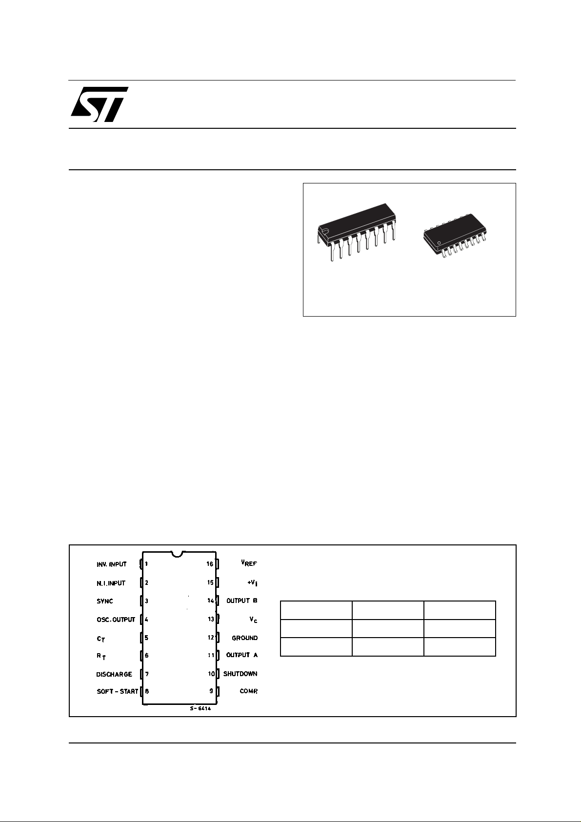
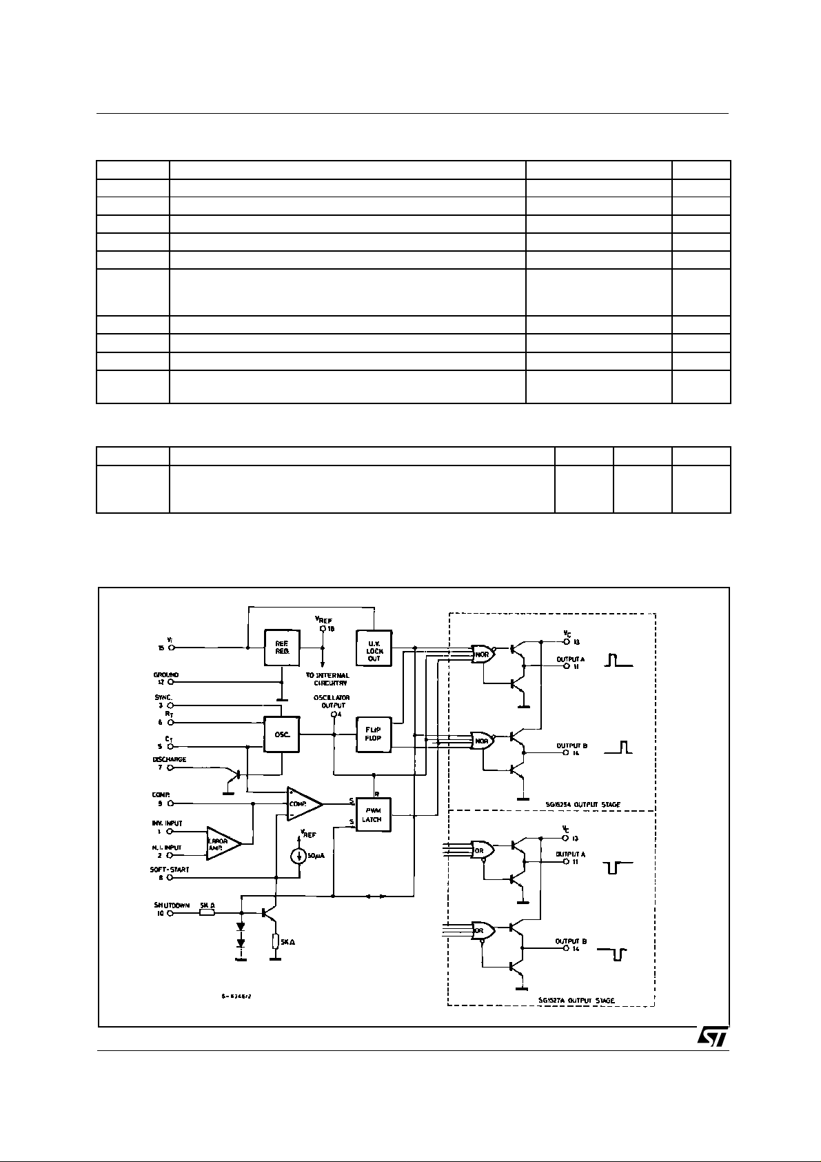
PIN CONNECTIONS AND ORDERING NUMBERS
SG2525A SG2525AN SG2525AP
SG3525A SG3525AN SG3525AP
June 2000
(top view)
Type Plastic DIP SO16
1/12
SG2525A-SG3525A
ABSOLUTE MAXIMUM RATINGS
Symbol Parameter Value Unit
V
V
I
OSC
I
o
I
R
I
T
P
tot
T
T
stg
T
op
THERMAL DATA
Symbol Parameter SO16 DIP16 Unit
R
th j-pins
R
th j-amb
R
th j-alumina
*
Thermal resistance junct ion-alumina with the devi ce soldered on the middle of an alumina supporting s ubstrate measuring 15 × 20 mm ; 0.65 mm
thickness with infinite heatsink.
Supply Voltage 40 V
i
Collector Supply Voltage 40 V
C
Oscillator Charging Current 5 mA
Output Current, Source or Sink 500 mA
Reference Output Current 50 mA
Current through CT Terminal
Logic Inputs
Analog Inputs
Total Power Dissipation at T
Junction Temperature Range – 55 to 150 °C
j
= 70 °C 1000 mW
amb
5
– 0.3 to + 5.5
– 0.3 to V
Storage Temperature Range – 65 to 150 °C
Operating Ambient Temperature :
SG3525A
SG2525A
– 25 to 85
0 to 70
Thermal Resistance Junction-pins Max
Thermal Resistance Junction-ambient Max
Thermal Resistance Junction-alumina (*) Max 50
i
50
80
°C/W
°C/W
°C/W
mA
V
V
°C
°C
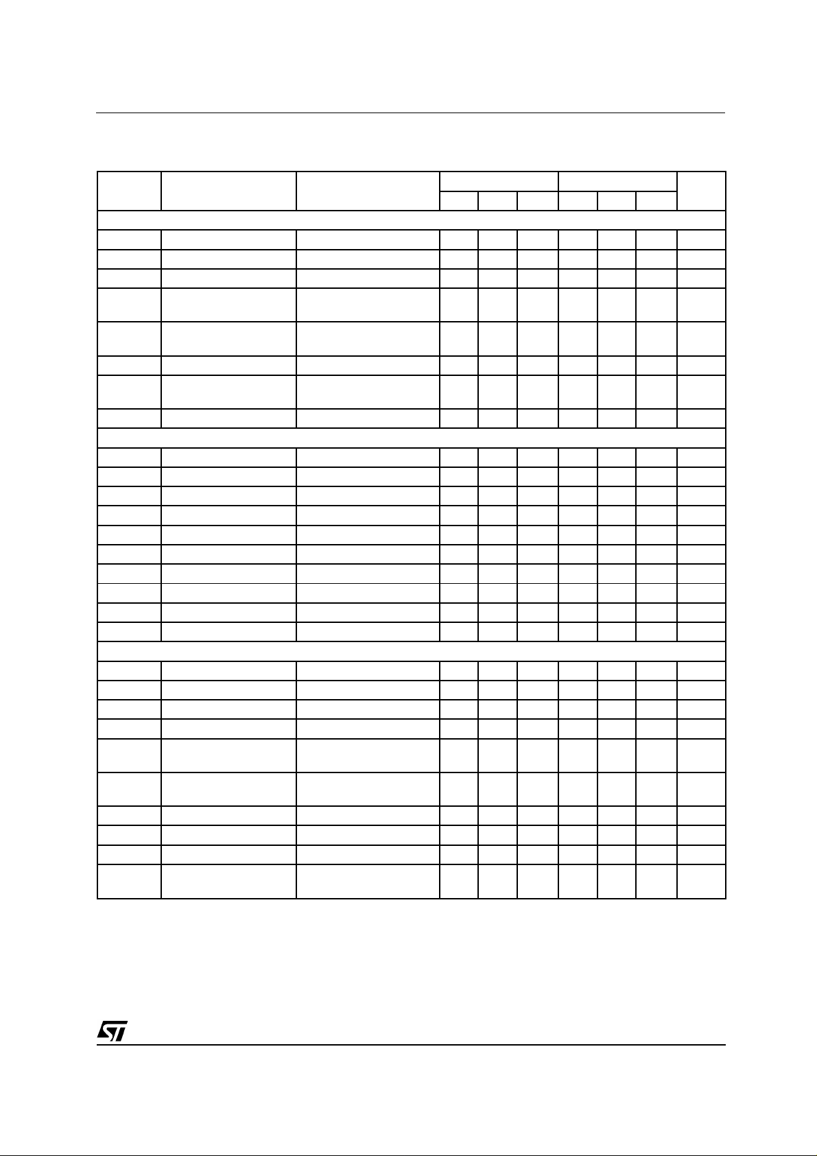
BLOCK DIAGRAM
2/12
SG2525A-SG3525A
ELECTRICAL CHARACTERISTICS
(V# i = 20 V, and ov er ope ra ti ng tem perature, unless other wise specified )
Symbol Parameter Test Conditions
REFERENCE SECTION
Output Voltage Tj = 25 °C 5.05 5.1 5.15 5 5.1 5.2 V
REF
Line Regulation Vi = 8 to 35 V 10 20 10 20 mV
REF
Load Regulation IL = 0 to 20 mA 20 50 20 50 mV
REF
/∆T* Temp. Stability Over Operating Range 20 50 20 50 mV
∆V
V
∆V
∆V
REF
* Total Output Variation Line, Load and
Temperature
Short Circuit Current V
= 0 Tj = 25 °C 80 100 80 100 mA
REF
* Output Noise Voltage 10 Hz ≤f ≤ 10 kHz,
T
= 25 °C
j
* Long Term Stability Tj = 125 °C, 1000 hrs 20 50 20 50 mV
∆V
REF
OSCILLATOR SECTION * *
*, • Initial Accuracy T
*, • Voltage Stability V
= 25 °C ± 2 ± 6 ± 2 ± 6%
j
= 8 to 35 V ± 0.3 ± 1 ± 1 ± 2%
i
∆f/∆T* Temperature Stability Over Operating Range ± 3 ± 6 ± 3 ± 6%
f
MIN
f
MAX
Minimum Frequency RT = 200 KΩ CT = 0.1 µ F 120 120 Hz
Maximum Frequency RT = 2 KΩ CT = 470 pF 400 400 KHz
Current Mirror I
= 2 mA 1.7 2 2.2 1.7 2 2.2 mA
RT
*, • Clock Amplitude 3 3.5 3 3.5 V
*, • Clock Width T
= 25 °C 0.3 0.5 1 0.3 0.5 1 µs
j
Sync Threshold 1.2 2 2.8 1.2 2 2.8 V
Sync Input Current Sync Voltage = 3.5 V 1 2.5 1 2.5 mA
ERROR AMPLIFIER SECTION (V
V
I
Input Offset Voltage 0.5 5 2 10 mV
OS
Input Bias Current 1 10 1 10 µA
I
b
Input Offset Current 1 1 µA
os
DC Open Loop Gain R
* Gain Bandwidth
= 5.1 V)
CM
≥ 10 MΩ 60 75 60 75 dB
L
= 0 dB Tj = 25 °C 1 2 1 2 MHz
G
v
Product
*, ❚ DC Transconduct. 30 KΩ ≤ R
T
= 25 °C
j
≤ 1 MΩ
L
Output Low Level 0.2 0.5 0.2 0.5 V
Output High Level 3.8 5.6 3.8 5.6 V
CMR Comm. Mode Reject. V
PSR Supply Voltage
= 1.5 to 5.2 V 60 75 60 75 dB
CM
= 8 to 35 V 50 60 50 60 dB
V
i
Rejection
SG2525A SG3525A
Min. Typ. Max. Min. Typ. Max.
5 5.2 4.95 5.25 V
40 200 40 200 µVrms
1.1 1.5 1.1 1.5 ms
Unit
3/12
SG2525A-SG3525A
ELECT RICAL CHARAC TE RI S TI CS
Symbol Parameter Test Conditions
(continued)
SG2525A SG3525A
Min. Typ. Max. Min. Typ. Max.
PWM COMPARATOR
Minimum Duty-cycle 0 0 %
• Maximum Duty-cycle 45 49 45 49 %
• Input Threshold Zero Duty-cycle 0.7 0.9 0.7 0.9 V
Maximum Duty-cycle 3.3 3.6 3.3 3.6 V
* Input Bias Current 0.05 1 0.05 1 µA
SHUTDOWN SECTION
Soft Start Current V
Soft Start Low Level V
Shutdown Threshold To outputs, V
Shutdown Input Current V
* Shutdown Delay V
OUTPUT DRIVERS (each output) (V
Output Low Level I
Output High Level I
Under-Voltage Lockout V
Collector Leakage VC = 35 V 200 200 µA
I
C
* Rise Time CL = 1 nF, Tj = 25 °C 100 600 100 600 ns
t
r
* Fall Time CL = 1 nF, Tj = 25 °C 50 300 50 300 ns
t
f
= 0 V, VSS = 0 V 255080255080 µA
SD
= 2.5 V 0.4 0.7 0.4 0.7 V
SD
= 5.1 V
T
= 25 °C
j
= 2.5 V 0.4 1 0.4 1 mA
SD
= 2.5 V Tj = 25 °C 0.2 0.5 0.2 0.5 µ s
SD
= 20 V)
C
= 20 mA 0.2 0.4 0.2 0.4 V
sink
= 100 mA 1 2 1 2 V
I
sink
= 20 mA 18 19 18 19 V
source
I
= 100 mA 17 18 17 18 V
source
and Vss = High 678678 V
comp
SS
0.6 0.8 1 0.6 0.8 1 V
TOTAL STANDBY CURRENT
Supply Current Vi = 35 V 14 20 14 20 mA
I
s
Unit
*
These parameters, although guaranteed over the rec ommend ed operating conditions, are not 10 0 % tes ted in p roduc tio n.
•
Tested at f
f =
DC transconductance (gM) relates to DC open-lo op voltage gain (Gv) according to t he f o ll owing equation : Gv = gM RL where RL is the resist ance
.
from pin 9 to ground . The m inimum g
= 40 KHz (RT = 3.6 KΩ, CT = 10nF, RD = 0 Ω). Approximate oscill ator f requency is defined by :
osc
1
(0.7 RT + 3 RD)
C
T
specification is used t o calcul ate m ini mum Gv when the error amplifi er output i s loade d.
M
4/12

TEST CIRCUIT
SG2525A-SG3525A
5/12

SG2525A-SG3525A
RECOMMENDED OPER ATING CONDITIONS (•)
Parameter Value
Input Voltage (V
Collector Supply Voltage (V
Sink/Source Load Current (steady state) 0 to 100 mA
Sink/Source Load Current (peak) 0 to 400 mA
Reference Load Current 0 to 20 mA
Oscillator Frequency Range 100 Hz to 400 KHz
Oscillator Timing Resistor 2 KΩ to 150 KΩ
Oscillator Timing Capacitor 0.001 µF to 0.1 µF
Dead Time Resistor Range 0 to 500 Ω
•
(⋅) Range over which the device is f unct i onal and pa rameter limits are guaranteed.
) 8 to 35 V
i
) 4.5 to 35 V
C
Figure 1 :
and C
Figure 3
Oscillator Charge Time vs. R
.
T
: Output Saturation
Characteristics.
T
Figure 2 :
and C
Figure 4
Oscillator Discharge Time vs. R
.
T
: Error Ampl if ier V oltage Gain and
D
Phase vs. Frequency.
6/12

SG2525A-SG3525A
Figure 5
: Error Ampl if ier .
PRINCIPLES OF OPERATION
SHUTDOWN OPTIONS (see Block Diagram)
Since both the compensation and soft-start termi-
nals (Pins 9 and 8) have current source pull-ups,
either can readily accept a pull-down signal which
only has to s ink a maxim um of 100 µA to turn off the
outputs. This is su bject to the added requir ement of
dischargi ng w hat ev e r e xter nal capacitanc e m ay b e
attached to these pins.
An alternat e approach is the u se of the shutdo wn circuitry of Pin 10 which has been improved to enhance the available shutdown options. Activating
this circuit by applying a positive signal on Pin 10
performs two functions : the PWM latch is immedi-
ately set providing the fastest turn-off signal to the
outputs ; and a 150 µA current sink begins to discharge the external soft-start capacitor. If the shutdown command is short, the PWM signal is terminated without significant discharge of the soft-start
capacitor, th us, allowing, fo r example, a conv enient
implementation of pulse-by-pulse current limiting.
Holding Pin 10 high for a longer durati on, h owever,
will ultimately discharge this external capacitor, recycling slow turn-on upon r elea se .
Pin 10 should not be left floating as noise pickup
could conc eiv a bly int er r upt nor m al operation.
7/12

SG2525A-SG3525A
Figure 6
: Oscilla tor S c he ma ti c .
Figure 7 :
Output Circuit (1/2 c ircuit shown).
8/12

SG2525A-SG3525A
Figure 8. Figure 9
For single-ended supplies, the driver outputs are
grounded. The V
terminal is s witched to g round by
C
the totem-po le source tran sistors on alternate os cillator cycles.
In conventional push-pull bipolar designs, forward
base drive is controlled by R1 - R3. Rapid turn-off
times for the power devices are achieved with
speed-up c apa ci t ors C
.
and C2.
1
Figure 10. Figure 11.
The low source impedance of the output driver s provides rapid charging of Power Mos input capacitance whi le m ini mi z ing external components.
Low power transformers can be driven directly.
Automatic re set occurs during dea d time, when both
ends of the primary winding a re switc hed to gro und.
9/12

SG2525A-SG3525A
DIM.
MIN. TYP. MAX. MIN. TYP. MAX.
a1 0.51 0.020
B 0.77 1.65 0.030 0.065
b 0.5 0.020
b1 0.25 0.010
D 20 0.787
E 8.5 0.335
e 2.54 0.100
e3 17.78 0.700
F 7.1 0.280
I 5.1 0.201
L 3.3 0.130
Z 1.27 0.050
mm inch
OUTLINE AND
MECHANICAL DATA
DIP16
10/12

SG2525A-SG3525A
DIM.
MIN. TYP. MAX. MIN. TYP. MAX.
A 1.75 0.069
a1 0.1 0.25 0.004 0.009
a2 1.6 0.063
b 0.35 0.46 0.014 0.018
b1 0.19 0.25 0.007 0.010
C 0.5 0.020
c1 45˚ (typ.)
D (1) 9.8 10 0.386 0.394
E 5.8 6.2 0.228 0.244
e 1.27 0.050
e3 8.89 0.350
F (1) 3.8 4 0.150 0.157
G 4.6 5.3 0.181 0.209
L 0.4 1.27 0.016 0.050
M 0.62 0.024
S
mm inch
8˚(max.)
OUTLINE AND
MECHANICAL DATA
SO16 Narrow
(1) D and F do not include mold flash or protrusions. Mold flash or potrusions shall not exceed 0.15mm (.006inch).
11/12

SG2525A-SG3525A
Information furnished is believed to be accurate and reliable. However, STMicroelectronics assumes no responsibility for the consequences of us e of such inform ation nor for any infringement of patent s or other right s of third parties whic h may result from its use. No
license is granted by implication or otherwise under any patent or patent rights of STMicroelectronics. Specification mentioned in this
publication are subject to change without notice. This publication supersedes and replaces all information pr eviously supplied. STMicroelectronics products are not authorized for use as critical components in life support devices or systems without express wr itten
approval of STMicr oelectronic s.
Australia - Brazil - Chin a - Finl and - France - Ger many - H ong Kong - In dia - Ital y - Japan - Mal aysia - Malta - M orocco -
The ST logo is a regis tered tradem ark of STMic roelec tronics
© 2000 S TMicroel ectroni cs – Printed i n Italy – Al l Rights Res erved
STMicroelectronic s GROUP OF COM PANIES
Singapore - Spain - Swede n - Swi tzerland - U nited K ingdom - U. S.A.
http://www.st.co m
12/12
 Loading...