


Advanced constant voltage and constant current controller
V
V
CC
with very efficient LED pilot-lamp driver
Features
■ Constant voltage and constant current control
■ Very efficient LED pilot-lamp driver
■ Wide operating V
■ Low quiescent consumption: 250 µA
■ Voltage reference: 2.5 V
■ Voltage control loop accuracy ± 0.5%
■ Current sense threshold: 50 mV
■ Current control loop accuracy ± 4%
■ Low external component count
■ Open-drain output stage
■ SOT23-6L package
Applications
■ AC-DC adapter with LED pilot-lamp
■ Battery chargers with LED pilot-lamp
■ SMPS with LED pilot-lamp
range (3.5 V - 36 V)
CC
SEA05L
Preliminary data
SOT23-6L (plastic package)
Figure 1.
The voltage reference, along with one op-amp, is
the core of the voltage control loop. The current
sensing circuit and the other op-amp make up the
current control loop.
Block diagram
2.5 V
1.23 V
50mV
2
GND
+
-
+
-
1
Isense
6
OSC
5
Out
3
ctrl
4
LD
Description
The external components needed to complete the
two control loops are:
The device is a highly integrated solution for
SMPS applications, with an LED pilot-lamp
requiring a dual control loop to perform CV
(constant voltage) and CC (constant current)
regulation.
The IC allows very efficient LED pilot-lamp driving
which helps to reduce the standby consumption of
the SMPS. It integrates a voltage reference, two
op-amps (with OR-ed open-drain outputs), a lowside current sensing circuit and an LED pilot-lamp
driver pin implemented with an open-drain mosfet
- a resistor divider that senses the output of the
power supply and fixes the voltage regulation
setpoint at the specified value
- a sense resistor that feeds the current sensing
circuit with a voltage proportional to the DC output
current; this resistor determines the current
regulation setpoint and must be adequately rated
in terms of power dissipation
- the frequency compensation components (R-C
networks) for both loops.
driven by square waveform with 12.5% duty cycle
at 1 kHz that allows reducing LED consumption.
February 2011 Doc ID 18462 Rev 1 1/12
This is preliminary information on a new product now in development or undergoing evaluation. Details are subject to
change without notice.
The device is ideal for space-critical applications.
Table 1. Device summary
Order code Package Packing
SEA05LTR SOT23-6L Tape & reel
www.st.com
1

Contents SEA05L
Contents
1 Operation . . . . . . . . . . . . . . . . . . . . . . . . . . . . . . . . . . . . . . . . . . . . . . . . . . 3
2 Application information . . . . . . . . . . . . . . . . . . . . . . . . . . . . . . . . . . . . . . 6
2.1 Voltage and current control . . . . . . . . . . . . . . . . . . . . . . . . . . . . . . . . . . . . 6
2.2 Compensation . . . . . . . . . . . . . . . . . . . . . . . . . . . . . . . . . . . . . . . . . . . . . . 8
2.3 LD pin function . . . . . . . . . . . . . . . . . . . . . . . . . . . . . . . . . . . . . . . . . . . . . . 8
3 Package mechanical data . . . . . . . . . . . . . . . . . . . . . . . . . . . . . . . . . . . . 10
4 Revision history . . . . . . . . . . . . . . . . . . . . . . . . . . . . . . . . . . . . . . . . . . . 11
2/12 Doc ID 18462 Rev 1
SEA05L Operation
1 Operation
Table 2. Absolute maximum ratings
Symbol Pin Parameter Value Unit
V
CC
Vout 5 Open-drain voltage –0.3 to V
Iout 5 Max. sink current 20 mA
V
LD
I
LD
Isense 1 Analog input –0.3 to V
Vctrl 3 Analog input –0.3 to V
1. Vctrl cannot exceed VCC and cannot exceed 12 V.
Table 3. Thermal data
Symbol Parameter Value Unit
R
th j-amb
Tj
op
Tstg Storage temperature –55 to 150
Figure 2. Pin configuration
6 DC supply voltage –0.3 to 38 V
CC
4 Open-drain voltage –0.3 to V
4 Max. sink current 15 mA
Thermal resistance, junction-to-ambient 250 °C/W
Junction temperature operating range –40 to 150
Isense
1
1
1
1
6
6
6
6
Vcc
CC
CC
CC
< 12
(1)
V
V
V
V
°C
GND
Vctrl
Table 4. Pin functions
Pin number Name Function
Inverting input of the current loop op-amp. The pin is typically used for the
1 Isense
2GND
current control loop, connecting it to the positive end of the current sense
resistor through a decoupling resistor.
Ground. Return of the bias current of the device. 0 V reference for all
voltages. The pin has to be tied as close as possible to the ground output
terminal of the converter to minimize load current effect on the voltage
regulation setpoint.
2
2
2
2
3
3
3
3
Doc ID 18462 Rev 1 3/12
5
5
5
5
4
4
4
4
Out
LD
AM04985v1
Operation SEA05L
Table 4. Pin functions (continued)
Pin number Name Function
Inverting input of the voltage loop op-amp. The pin is typically used for the
3Vctrl
4LD
5OUT
6V
voltage control loop and is connected to the midpoint of a resistor divider
that senses the output voltage.
Open-drain output able to sink 5 mA (peak), driven by the internal oscillator
at 1 kHz square waveform with 12.5% duty cycle. The internal mosfet starts
to switch when V
is above the turn-on threshold (typ. 3 V) and it is off (LD
CC
high impedance) when VCC is below the UVLO of the IC. The pin can be
connected to an external LED pilot-lamp with a resistor in series in order to
limit the LED current
Common open-drain output of the two internal op-amps. The pin, only able
to sink current, is typically connected to the branch of the optocoupler's
photodiode to transmit the error signal to the primary side.
Supply voltage of the device. A small bypass capacitor (0.1 µF typ.) to GND,
located as close to the IC pins as possible, might be useful to get a clean
CC
supply voltage.
4/12 Doc ID 18462 Rev 1

SEA05L Operation
Table 5. Electrical characteristics (–25 C° < Tj < 125 °C, VCC = 20 V; unless otherwise specified)
Symbol Parameter Test condition Min. Typ. Max. Unit
Device supply
V
Voltage operating range 3.5 36 V
CC
Quiescent current
I
CC
(Ictrl = Vsense = 0, OUT = open)
250 500 µA
Voltage control loop op-amp
(2)
(1)
13.5 S
Tj = 25 °C 2.488 2.5 2.512 V
Gm
Transconductance (sink current only)
v
Vctrl Voltage reference default value
Ibias Inverting input bias current 25 nA
Current control loop
Gm
V
csth
Transconductance (sink current only)
i
Current sense threshold at I(Iout) = 1 mA
(3)
(4)
1.5 7 S
48 50 52 mV
Ibias Non-inverting input source current 6 µA
Output stage
V
OUTlow
Low output level at 2 mA sink current 200 400 mV
LED driver
I
LED driver sink current capability (peak) 10 mA
LD
f
LED driver current modulation frequency 0.6 1 1.4 kHz
LD
V
I
LD_LKG
1. If the voltage on Vctrl (the negative input of the amplifier) is higher than the positive amplifier input, and it is increased by
2. The internal voltage reference is set at 2.5 V. The voltage control loop precision takes into account the cumulative effects of
3. When the inverting input at Isense is greater than 50 mV, and the voltage is increased by 1 mV, the sinking current at the
4. The internal current sense threshold is triggered when the voltage on pin Isense is 50 mV. The current control loop
Low output level at 5 mA sink current
LDlow
(internal mosfet on)
LED driver leakage current
(internal mosfet off)
1mV, the sinking current at the output OUT will be increased by 3.5 mA.
the internal voltage reference deviation as well as the input offset voltage of the transconductance operational amplifier.
The internal voltage reference is fixed by bandgap, and trimmed to 0.48 % accuracy at room temperature.
output Out will be increased by 7 mA.
precision takes into account the cumulative effects of the internal voltage reference deviation as well as the input offset
voltage of the transconductance operational amplifier.
450 900 mV
0.5 µA
Doc ID 18462 Rev 1 5/12

Application information SEA05L
V
4
V
2 Application information
Figure 3. Typical application schematic
0.1μF
LED
cc
1.23 V
2.5 V
6
+
-
50mV
+
-
2
GND
Rsense
Io
1
Isense
=
V
O
OSC
2.1 Voltage and current control
Voltage control
R1
5
Out
3
05.0
sense
Vo
V
AM04986v1
ctrl
R2
LD
+
RR
21
V
R
5.2*
2
=
I
max
O
R
The voltage loop is controlled via a transconductance operational amplifier, the voltage
divider R
choose the values of R
, R2, and the optocoupler which is directly connected to the output. It is possible to
1
and R2 resistors using Equation 1 and Equation 2:
1
Equation 1
)(
RR
+
VctrlV
O
∗=
21
R
2
Equation 2
)(
VctrlV
+
RR
where V
As an example, with R
6/12 Doc ID 18462 Rev 1
O
∗=
21
Vctrl
is the desired output voltage.
O
= 100 kΩ and R2 = 15 kΩ VO = 19.17 V.
1

SEA05L Application information
Current control
The current loop is controlled via a transconductance operational amplifier, the sense
resistor R
The control equation verifies:
Equation 3
Equation 4
R
=
sense
, and the optocoupler.
sense
VIR =∗
max
V
I
csthOsense
csth
maxO
where I
control loop. As an example, with I
Note that the R
(P
) through it during full load operation.
lim
is the desired limited current, and V
Omax
omax
resistor should be chosen, taking into account the maximum dissipation
sense
= 1 A, V
is the threshold voltage for the current
csth
= 50 mV, then R
csth
sense
= 50 mΩ.
Equation 5
IVP ∗=
maxlim Ocsth
As an example, with I
= 1 A and V
Omax
= 50 mV, P
csth
= 50 mW.
lim
Therefore, for most adaptor and battery charger applications, a low-power resistor is
suitable for the current sensing function.
V
threshold is achieved internally by a voltage divider tied to an internal precise voltage
csth
reference. Its midpoint is tied to the positive input of the current control operational amplifier,
and its endpoint is connected to GND. The resistors of this voltage divider are matched to
provide the best precision possible. The current sinking outputs of the two transconductance
operational amplifiers are common (to the output of the IC). This makes an OR function
which ensures that whenever the current or the voltage reaches excessively high values, the
optocoupler is activated.
The relationship between the controlled current and the controlled output voltage can be
described with a square characteristic as shown in the following V/I output-power graph
(with power supply of the device independent from the output voltage).
Doc ID 18462 Rev 1 7/12

Application information SEA05L
Figure 4. Output voltage versus output current
Vout
Voltage regulation
Current regulation
2.2 Compensation
The voltage control transconductance operational amplifier can be fully compensated. Both
its output and negative input are directly accessible for external compensation components.
2.3 LD pin function
The device provides a unique feature that allows highly efficient driving of an LED pilot-lamp.
The main benefit of this new feature is to allow reducing the standby power consumption of
the SMPS with the LED pilot-lamp.
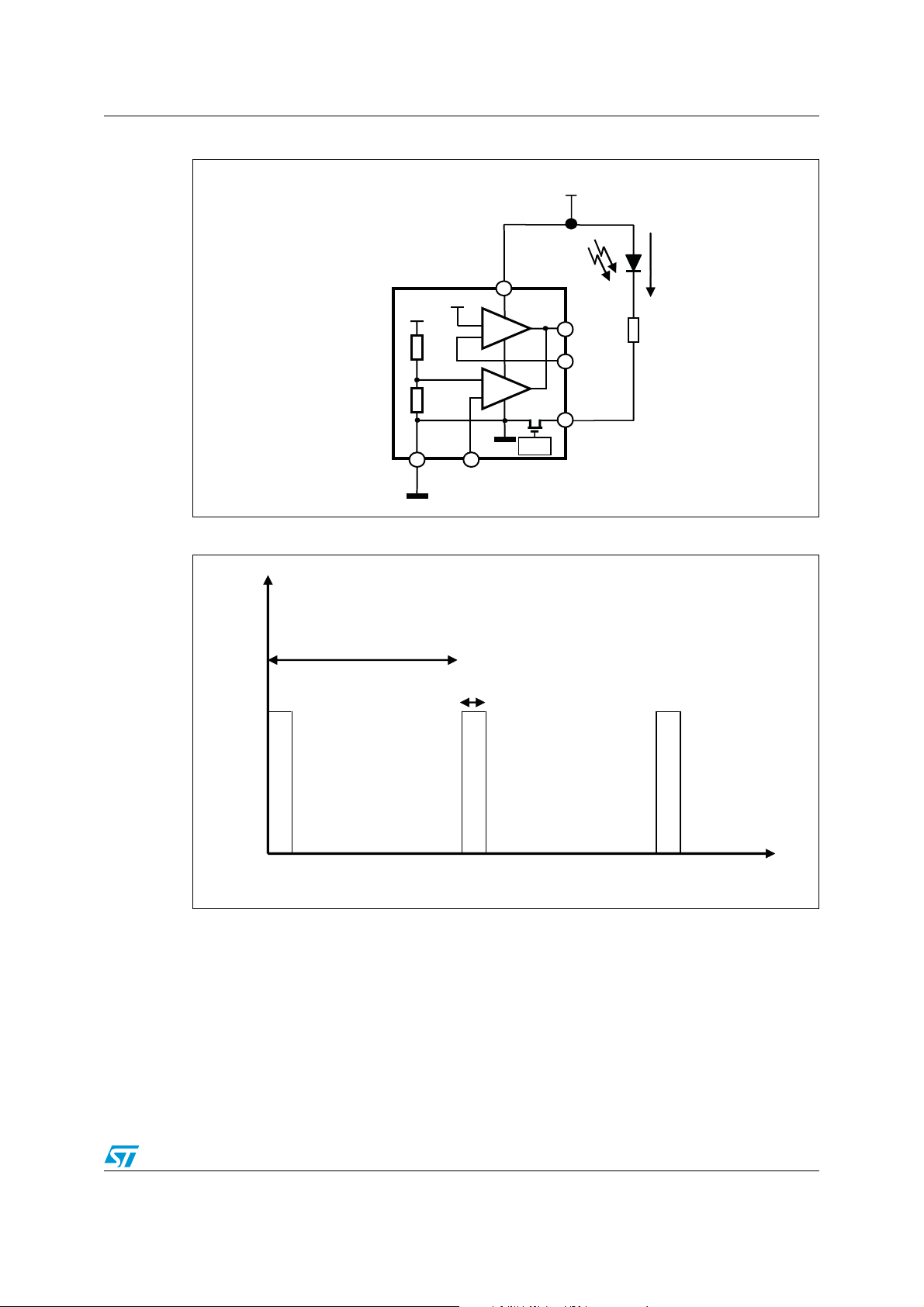
The LD pin is an open-drain output able to sink 5 mA (peak), driven by the internal oscillator
at 1 kHz (typ.) square waveform with 12.5% duty cycle (see Figure 6). The internal mosfet
starts to switch when V
impedance) when V
Connecting the LED pilot-lamp, with a resistor in series in order to limit the LED current, to
pin LD (as shown in Figure 5) reduces the power consumption of the LED while keeping the
same driving peak current. The LED driving current modulation frequency of 1 kHz (typ.)
eliminates the visual perception of flickering.
CC
(
Vcc of the device independent from output voltage)
is above the turn-on threshold (typ 3 V) and it is off (LD high
CC
Iout
is below the UVLO of the IC.
AM04987v1
8/12 Doc ID 18462 Rev 1
SEA05L Application information
V
V
Figure 5. Connection of LED to pin LD
cc
1.23 V
GND
2.5 V
50mV
+
-
+
-
1 2
Isen se
cc
6
OSC
LED
5
Out
3
Vctrl
4
LD
I
LED
R
LED
Figure 6. LED current waveform with a typical frequency of 1 kHZ
I
T=1ms (f=1kHz)
ton=125 µs (T/8)
I
LED
AM04988v1
t
AM04989v1
Doc ID 18462 Rev 1 9/12

Package mechanical data SEA05L
3 Package mechanical data
In order to meet environmental requirements, ST offers these devices in different grades of
ECOPACK
specifications, grade definitions and product status are available at: www.st.com.
ECOPACK
Table 6. SOT23-6L (2.90 mm x 2.80 mm) package mechanical data
®
packages, depending on their level of environmental compliance. ECOPACK®
®
is an ST trademark.
Sym
Min Typ Max Min Typ Max
A 1.45 0.057
A1 0.00 0.15 0.000 0.006
A2 0.90 1.15 1.30 0.035 0.045 0.051
b 0.30 0.50 0.012 0.020
c 0.08 0.22 0.003 0.009
D 2.90 0.114
E 2.80 0.110
E1 1.60 0.063
e 0.95 0.037
e1 1.90 0.075
L 0.30 0.45 0.60 0.012 0.018 0.024
è 0° 4° 8° 0° 4° 8°
N 6 6
mm inches
Note: Dimensions per JEDEC MO178AB
Figure 7. SOT23-6L (2.90 mm x 2.80 mm) package mechanical drawing
10/12 Doc ID 18462 Rev 1
7049717_G

SEA05L Revision history
4 Revision history
Table 7. Document revision history
Date Revision Changes
23-Feb-2011 1 Initial release.
Doc ID 18462 Rev 1 11/12

SEA05L
Please Read Carefully:
Information in this document is provided solely in connection with ST products. STMicroelectronics NV and its subsidiaries (“ST”) reserve the
right to make changes, corrections, modifications or improvements, to this document, and the products and services described herein at any
time, without notice.
All ST products are sold pursuant to ST’s terms and conditions of sale.
Purchasers are solely responsible for the choice, selection and use of the ST products and services described herein, and ST assumes no
liability whatsoever relating to the choice, selection or use of the ST products and services described herein.
No license, express or implied, by estoppel or otherwise, to any intellectual property rights is granted under this document. If any part of this
document refers to any third party products or services it shall not be deemed a license grant by ST for the use of such third party products
or services, or any intellectual property contained therein or considered as a warranty covering the use in any manner whatsoever of such
third party products or services or any intellectual property contained therein.
UNLESS OTHERWISE SET FORTH IN ST’S TERMS AND CONDITIONS OF SALE ST DISCLAIMS ANY EXPRESS OR IMPLIED
WARRANTY WITH RESPECT TO THE USE AND/OR SALE OF ST PRODUCTS INCLUDING WITHOUT LIMITATION IMPLIED
WARRANTIES OF MERCHANTABILITY, FITNESS FOR A PARTICULAR PURPOSE (AND THEIR EQUIVALENTS UNDER THE LAWS
OF ANY JURISDICTION), OR INFRINGEMENT OF ANY PATENT, COPYRIGHT OR OTHER INTELLECTUAL PROPERTY RIGHT.
UNLESS EXPRESSLY APPROVED IN WRITING BY AN AUTHORIZED ST REPRESENTATIVE, ST PRODUCTS ARE NOT
RECOMMENDED, AUTHORIZED OR WARRANTED FOR USE IN MILITARY, AIR CRAFT, SPACE, LIFE SAVING, OR LIFE SUSTAINING
APPLICATIONS, NOR IN PRODUCTS OR SYSTEMS WHERE FAILURE OR MALFUNCTION MAY RESULT IN PERSONAL INJURY,
DEATH, OR SEVERE PROPERTY OR ENVIRONMENTAL DAMAGE. ST PRODUCTS WHICH ARE NOT SPECIFIED AS "AUTOMOTIVE
GRADE" MAY ONLY BE USED IN AUTOMOTIVE APPLICATIONS AT USER’S OWN RISK.
Resale of ST products with provisions different from the statements and/or technical features set forth in this document shall immediately void
any warranty granted by ST for the ST product or service described herein and shall not create or extend in any manner whatsoever, any
liability of ST.
ST and the ST logo are trademarks or registered trademarks of ST in various countries.
Information in this document supersedes and replaces all information previously supplied.
The ST logo is a registered trademark of STMicroelectronics. All other names are the property of their respective owners.
© 2011 STMicroelectronics - All rights reserved
STMicroelectronics group of companies
Australia - Belgium - Brazil - Canada - China - Czech Republic - Finland - France - Germany - Hong Kong - India - Israel - Italy - Japan -
Malaysia - Malta - Morocco - Philippines - Singapore - Spain - Sweden - Switzerland - United Kingdom - United States of America
www.st.com
12/12 Doc ID 18462 Rev 1
 Loading...