

现货库存、技术资料、百科信息、热点资讯,精彩尽在鼎好!
1
2
3
45
6
7
8
Features
■ Low turn off time
■ Maximum operating frequency greater than
500kHz
■ Timing from microseconds to hours
■ Operates in both astable and monostable
modes
■ High output current can source or sink 200mA
■ Adjustable duty cycle
■ TTL compatible
■ Temperature stability of 0.005% per °C
Description
NE555
SA555 - SE555
General purpose single bipolar timers
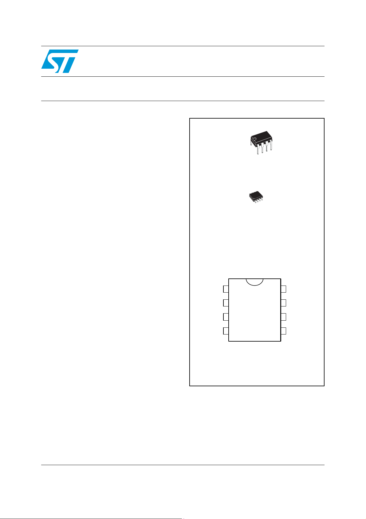
N
DIP8
(Plastic package)
D
SO8
(Plastic micropackage)
The NE555 monolithic timing circuit is a highly
stable controller capab le of producing accurate
time delays or oscillation. In the time delay mode
of operation, the time is precisely controlled by
one external resistor and capacitor. For a stable
operation as an oscillator, the free running
frequency and the duty cycle are both accurately
controlled with two external resistors and one
capacitor.
The circuit may be triggered and reset on falling
wav eforms, and the output structure can source
or sink up to 200mA.
Pin connections
(top view)
1 - GND
2 - Trigger
3 - Output
4 - Reset
5 - Control voltage
6 - Threshold
7 - Discharge
8 - V
CC
March 2007 Rev 4 1/20
www.st.com
20

Contents NE555 - SA555 - SE555
Contents
1 Schematic diagrams . . . . . . . . . . . . . . . . . . . . . . . . . . . . . . . . . . . . . . . . . 3
2 Absolute maximum ratings and operating conditions . . . . . . . . . . . . . 4
3 Electrical characteristics . . . . . . . . . . . . . . . . . . . . . . . . . . . . . . . . . . . . . 5
4 Application information . . . . . . . . . . . . . . . . . . . . . . . . . . . . . . . . . . . . . . 9
4.1 Monostable operation . . . . . . . . . . . . . . . . . . . . . . . . . . . . . . . . . . . . . . . . . 9
4.2 Astable operation . . . . . . . . . . . . . . . . . . . . . . . . . . . . . . . . . . . . . . . . . . . 10
4.3 Pulse width modulator . . . . . . . . . . . . . . . . . . . . . . . . . . . . . . . . . . . . . . . 13
4.4 Linear ramp . . . . . . . . . . . . . . . . . . . . . . . . . . . . . . . . . . . . . . . . . . . . . . . 13
4.5 50% duty cycle oscillator . . . . . . . . . . . . . . . . . . . . . . . . . . . . . . . . . . . . . 14
4.6 Additional information . . . . . . . . . . . . . . . . . . . . . . . . . . . . . . . . . . . . . . . . 15
5 Package information . . . . . . . . . . . . . . . . . . . . . . . . . . . . . . . . . . . . . . . . 16
6 Ordering information . . . . . . . . . . . . . . . . . . . . . . . . . . . . . . . . . . . . . . . 19
7 Revision history . . . . . . . . . . . . . . . . . . . . . . . . . . . . . . . . . . . . . . . . . . . 19
2/20
NE555 - SA555 - SE555 Schematic diagrams
T
1 Schematic diagrams
Figure 1. Block diagram
+
V
CC
5kΩ
THRESHOLD
CONTROL VOLTAGE
TRIGGER
COMP
5kΩ
COMP
5kΩ
R
FLIP-FLOP
S
INHIBIT/
RESET
Q
DISCHARGE
OUT
Figure 2. Schematic diagram
THRESHOLD
COMPARATOR
V
HRESHOLD
TRIGGER
RESET
DISCHARGE
G N D
CC
R1
4.7k
Q5 Q6 Q7 Q8 Q9
Q1
Q2
2
4
Q15
7
Q14
1
R2
R3
830
W
W
Q3
R5
10k
4.7k
Q4
Q10
W
RESET
W
R6
100k
Q11 Q12
W
S - 8086
R4
1k
W
Q13
100k
S
CONTROL
VOLTAGE
5
R8
5k
W
Q19
R11
5k
W
R9
5k
W
R7
W
D2
Q16 Q18
Q17
R10
5k
W
4.7k
R17
R12
6.8k
W
Q20
W
Q23
R16
100
Q21
OUTPUT
Q22
R13
3.9k
W
D1
R14
220
R15
4.7k
W
3
W
Q24
W
TRIGGER COMPARATOR FLIP FLOP
3/20
Absolute maximum ratings and operating conditions NE555 - SA555 - SE555
2 Absolute maximum ratings and operating conditions
Table 1. Absolute maximum ratings
Symbol Parameter Value Unit
V
CC
T
j
T
stg
Table 2. Operating conditions
Supply voltage 18 V
Junction temperature 150 °C
Storage temperature range -65 to 150 °C
Symbol Parameter Value Unit
Supply voltage
Vth, V
V
trig
CC
, Vcl, V
NE555
SA555
SE555
Maximum input voltage V
reset
4.5 to 16
4.5 to 16
4.5 to 18
CC
Operating free air temperature range
T
oper
NE555
SA555
SE555
0 to 70
-40 to 105
-55 to 125
V
V
°C
4/20

NE555 - SA555 - SE555 Electrical characteristics
3 Electrical characteristics
Table 3. T
= +25°C, VCC = +5V to +15V (unless otherwise specified)
amb
Symbol Parameter
Supply current (RL = ∝)
I
Low stage V
CC
High state V
= +5V
CC
VCC = +15V
= 5V
CC
Timing error (monostable)
(R
= 2k to 100kΩ, C = 0.1μF)
A
Initial accuracy
(1)
Drift with temperature
Drift with supply voltage
Timing error (astable)
(R
= 1kΩ to 100kΩ, C = 0.1μF, VCC = +15V)
A, RB
Initial accuracy -
(1)
Drift with temperature
Drift with supply voltage
Control voltage level
V
CL
VCC = +15V
= +5V
V
CC
Threshold voltage
V
th
V
CC
= +15V
VCC = +5V
Threshold current
I
th
(2)
Trigger voltage
V
V
I
trig
reset
trig
VCC = +15V
= +5V
V
CC
Trigger current (V
Reset voltage
(3)
= 0V) 0.5 0.9 0.5 2.0 µA
trig
Reset current
I
reset
V
V
reset
reset
= +0.4V
= 0V
Low level output voltage
= +15VI
V
CC
V
OL
VCC = +5V I
O(sink)
I
O(sink)
I
O(sink)
I
O(sink)
O(sink)
I
O(sink)
= 10mA
= 50mA
= 100mA
= 200mA
= 8mA
= 5mA
High level output voltage
V
= +15VI
V
OH
CC
V
CC
= +5V I
O(sink)
I
O(sink)
O(sink)
= 200mA
= 100mA
= 100mA
SE555 NE555 - SA555
Min. Typ. Max. Min. Typ. Max.
3
10
2
0.5
30
0.05
1.5
90
0.15
9.6
2.9103.33
9.4
2.7103.33
5
12
3
10
2
2
100
0.2
1
50
0.130.5
2.25
150
0.3
10.4
3.892.6103.33114
10.648.8
2.4103.33
6
15
ppm/°C
ppm/°C
11.2
4.2
0.1 0.25 0.1 0.25 µA
4.8
1.4551.67
5.2
1.9
4.5
1.151.67
5.6
2.2
0.4 0.7 1 0.4 0.7 1 V
13
0.1
0.4
0.1
0.4
2.5
0.1
0.05
12.5
13.3
3
3.3
0.4
1
0.15
0.5
2
2.2
0.1
0.4
0.1
0.4
2
0.4
1.5
0.25
0.75
2.5
2.5
0.25
0.2
0.3
0.25
0.4
0.35
12.5
12.75
2.75
13.3
3.3
Unit
mA
%
%/V
%
%/V
V
V
V
mA
V
V
5/20
Electrical characteristics NE555 - SA555 - SE555
Table 3. T
= +25°C, VCC = +5V to +15V (unless otherwise specified)
amb
SE555 NE555 - SA555
Symbol Parameter
Min. Typ. Max. Min. Typ. Max.
I
dis(off)
V
dis(sat)
t
1. Tested at VCC = +5V and VCC = +15V.
2. This will determine the maximum value of R
operation and 3.5MΩ for +5V operation.
3. Specified with trigger input high.
4. No protection against excessive pin 7 current is necessary, providing the package dissipation rating is not exceeded.
5. Time measured from a positive pulse (from 0V to 0.8xV
Output pin. Trigger is tied to Threshold.
Discharge pin leakage current
(output high) V
Discharge pin saturation voltage
(output low)
VCC = +15V, I
VCC = +5V, I
t
Output rise time
r
t
Output fall time
f
Turn off time
off
(4)
(5)
dis
dis
dis
(V
= 10V
= 15mA
= 4.5mA
= VCC)0.50.5µs
reset
+ RB for 15V operation. The maximum total (RA + RB) is 20MΩ for 15V
A
) on the Threshold pin to the transition from high to low on the
CC
20 100 20 100 nA
18080480
200
100
100
200
200
18080480
200
100
100
300
300
Unit
mV
ns
6/20
 Loading...