

ST NE556, SA556, SE556 User Manual

Features
■ Low turn-off time
■ Maximum operating frequency greater than
500 kHz
■ Timing from microseconds to hours
■ Operates in both astable and monostable
modes
■ Output can source or sink up to 200 mA
■ Adjustable duty cycle
■ TTL compatible
■ Temperature stability of 0.005% per °C
Description
NE556
SA556 - SE556
General-purpose dual bipolar timers
N
DIP14
(Plastic package)
D
SO14
(Plastic micropackage)
The NE556, SA556 and SE556 dual monolithic
timing circuits are highly stable controllers
capable of producing accurate time delays or
oscillation. In the time delay mode of operation,
the time is precisely controlled by one external
resistor and capacitor. For a stable operation as
an oscillator, the free running frequency and the
duty cycle are both accurately controlled with two
external resistors and one capacitor.
The circuits may be triggered and reset on falling
waveforms, and the output structure can source
or sink up to 200 mA.
Discharge
Threshold
Control Voltage
Reset
Output
Trigger
GND
Pin connections
(top view)
1
2
3
4
5
6
7
14
V
Discharge
13
Threshold
12
Control Voltage
11
Reset
10
Output
9
Trigger
8
CC
January 2009 Rev 2 1/16
www.st.com
16
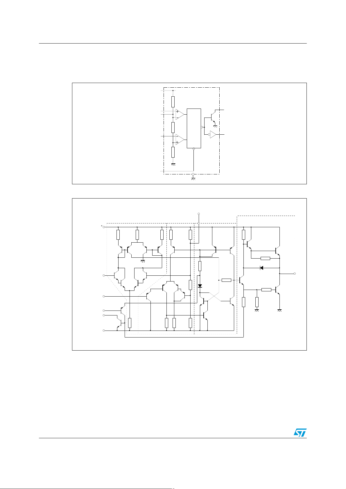
Schematic diagrams NE556 - SA556 - SE556
6
T
1 Schematic diagrams
Figure 1. Block diagram
+
V
CC
W
5k
THRESHOLD
CONTROL VOLTAGE
TRIGGER
COMP
W
5k
COMP
W
5k
R
FLIP-FLOP
S
INHIBIT/
RESET
Q
DISCHARGE
OUT
1/2 NE55
RESET
Figure 2. Schematic diagram
THRESHOLD
COMPARATOR
V
HRESHOLD
TRIGGER
RESET
DISCHARGE
G N D
CC
R1
4.7k
Q5 Q6 Q7 Q8 Q9
Q1
Q2
2
4
Q15
7
Q14
1
R2
830
W
W
Q3
R5
10k
4.7k
Q4
Q10
W
S
CONTROL
VOLTAGE
5
R3
100k
W
R6
Q11 Q12
W
R4
R8
1k
5k
W
W
Q19
R11
5k
W
Q13
100k
R9
5k
W
R7
W
D2
Q16 Q18
Q17
R10
5k
W
4.7k
R17
R12
6.8k
W
Q20
W
Q23
R16
100
Q21
OUTPUT
Q22
R13
3.9k
W
D1
R14
220
R15
4.7k
W
3
W
Q24
W
TRIGGER COMPARATOR FLIP FLOP
2/16

NE556 - SA556 - SE556 Absolute maximum ratings and operating conditions
2 Absolute maximum ratings and operating conditions
Table 1. Absolute maximum ratings
Symbol Parameter Value Unit
V
CC
I
OUT
R
thja
R
thjc
ESD
Supply voltage 18 V
Output current (sink and source) ±225 mA
(1)
(1)
80
105
33
31
1000
150
1500
°C/W
°C/W
VMachine model (MM)
Thermal resistance junction to ambient
DIP14
SO-14
Thermal resistance junction to case
DIP14
SO-14
Human body model (HBM)
Charged device model (CDM)
(2)
(3)
(4)
Latch-up immunity 200 mA
T
LEAD
T
j
T
stg
1. Short-circuits can cause excessive heating. These values are typical and valid only for a single layer PCB.
2. Human body model: a 100 pF capacitor is charged to the specified voltage, then discharged through a
1.5kΩ resistor between two pins of the device. This is done for all couples of connected pin combinations
while the other pins are floating.
3. Machine model: a 200 pF capacitor is charged to the specified voltage, then discharged directly between
two pins of the device with no external series resistor (internal resistor < 5 Ω). This is done for all couples of
connected pin combinations while the other pins are floating.
4. Charged device model: all pins and the package are charged together to the specified voltage and then
discharged directly to the ground through only one pin. This is done for all pins.
Table 2. Operating conditions
Lead temperature (soldering 10 seconds) 260 °C
Junction temperature 150 °C
Storage temperature range -65 to 150 °C
Symbol Parameter Value Unit
Supply voltage
V
CC
NE556
SA556
SE556
, V
cl
th
, V
I
OUT
trig
reset
,
Maximum input voltage V
Output current (sink and source) ±200 mA
V
V
4.5 to 16
4.5 to 16
4.5 to 18
CC
Operating free air temperature range
T
oper
NE556
SA556
SE556
0 to 70
-40 to 105
-55 to 125
°C
3/16
V
V

Electrical characteristics NE556 - SA556 - SE556
3 Electrical characteristics
Table 3. T
= +25° C, VCC = +5 V to +15 V (unless otherwise specified)
amb
Symbol Parameter
Supply current (RL ∝) (2 timers)
I
Low state V
CC
High State V
= +5V
CC
VCC = +15V
= +5V
CC
Timing error (monostable)
(R
= 2kΩ to 100kΩ, C = 0.1μF)
A
Initial accuracy
(1)
Drift with temperature
Drift with supply voltage
Timing error (astable)
, RB = 1kΩ to 100kΩ, C = 0.1μF, VCC= +15V)
(R
A
Initial accuracy
(1)
Drift with temperature
Drift with supply voltage
Control voltage level
V
CL
V
CC
= +15V
VCC = +5V
Threshold voltage
V
th
I
th
VCC = +15V
= +5V
V
CC
Threshold current
(2)
Trigger voltage
V
trig
I
trig
V
reset
= +15V
V
CC
= +5V
V
CC
Trigger current (V
Reset voltage
(3)
= 0V) 0.5 0.9 0.5 2.0 µA
trig
Reset current
I
reset
V
V
reset
reset
= +0.4V
= 0V
Low level output voltage
VCC = +15V I
V
OL
= +5V I
V
CC
O(sink)
I
O(sink)
I
O(sink)
I
O(sink)
O(sink)
I
O(sink)
= 10mA
= 50mA
= 100mA
= 200mA
= 8mA
= 5mA
High level output voltage
= +15V I
V
V
OH
CC
= +5V I
V
CC
O(sink)
I
O(sink)
O(sink)
= 200mA
= 100mA
= 100mA
SE556 NE556 - SA556
Min. Typ. Max. Min. Typ. Max.
6
20
4
0.5
30
0.05
1.5
90
0.15
9.6
2.9103.33
9.4
2.7103.33
10
24
2
100
0.2
10.4
3.892.6103.33114
10.648.8
2.4103.33
6
20
4
1
50
0.130.5
2.25
150
0.3
11.2
12
30
ppm/°C
ppm/°C
4.2
0.1 0.25 0.1 0.25 µA
4.8
1.4551.67
5.2
1.9
4.5
1.151.67
5.6
2.2
0.4 0.7 1 0.4 0.7 1 V
13
3
0.1
0.4
0.1
0.4
2.5
0.1
0.05
12.5
13.3
3.3
0.4
1
0.15
0.5
2
2.2
0.1
0.4
0.1
0.4
2
0.4
1.5
0.25
0.75
2.5
2.5
0.25
0.2
0.3
0.25
0.4
0.35
12.5
12.75
2.75
13.3
3.3
Unit
mA
%
%/V
%
%/V
V
V
V
mA
V
V
4/16

NE556 - SA556 - SE556 Electrical characteristics
Table 3. T
= +25° C, VCC = +5 V to +15 V (unless otherwise specified) (continued)
amb
SE556 NE556 - SA556
Symbol Parameter
Unit
Min. Typ. Max. Min. Typ. Max.
I
dis(off)
V
dis(sat)
1. Tested at V
2. This will determine the maximum value of R
the max total R = 3.5 MΩ
3. Specified with trigger input high
4. No protection against excessive pin 7 current is necessary, providing the package dissipation rating will not be exceeded
5. Time measured from a positive going input pulse from 0 to 0.8 x V
output trigger is tied to threshold.
Discharge pin leakage current (output high)
= 10V)
(V
dis
Discharge pin saturation voltage (output low)
VCC = +15V, I
VCC = +5V, I
Output rise time
t
r
t
Output fall time
f
toff Turn-off time
= +5 V and VCC = +15 V
CC
(5)
dis
dis
(V
= 15mA
= 4.5mA
= VCC)0.50.5µs
reset
20 100 20 100 nA
(4)
18080480
200
100
100
+ RB for +15V operation the max total is R = 20 MΩ and for +5 V operation
A
into the threshold to the drop from high to low of the
CC
200
200
18080480
200
100
300
100
300
mV
ns
5/16
 Loading...