


Rad-hard adjustable positive voltage regulator
Features
■ 3 A low dropout voltage
■ Embedded overtemperature and overcurrent
protection
■ Adjustable overcurrent limitation
■ Output overload monitoring/signalling
■ Adjustable output voltage
■ Inhibit (ON/OFF) TTL-compatible control
■ Programmable output short-circuit current
■ Remote sensing operation
■ Rad-hard: guaranteed up to 300 krad Mil Std
883E Method 1019.6 high dose rate and 0.01
rad/s in ELDRS conditions
■ Heavy ion, SEL immune
FLAT-16
RHFL4913A
SMD5C:
5-connection SMD
Description
The RHFL4913A high-performance adjustable
positive voltage regulator provides exceptional
radiation performance. It is tested in accordance
with Mil Std 883E Method 1019.6, in ELDRS
conditions. The device is available in the FLAT-16
and the new SMD5C hermetic ceramic package,
and the QML-V die is specifically designed for
space and harsh radiation environments. It
operates with an input supply of up to 12 volts.
The RHFL4913A is QML-V qualified, DSCC SMD
#5962F02524.
December 2011 Doc ID 10005 Rev 14 1/20
www.st.com
20

Contents RHFL4913A
Contents
1 Diagram . . . . . . . . . . . . . . . . . . . . . . . . . . . . . . . . . . . . . . . . . . . . . . . . . . . 3
2 Pin configuration . . . . . . . . . . . . . . . . . . . . . . . . . . . . . . . . . . . . . . . . . . . . 4
3 Maximum ratings . . . . . . . . . . . . . . . . . . . . . . . . . . . . . . . . . . . . . . . . . . . . 5
4 Electrical characteristics . . . . . . . . . . . . . . . . . . . . . . . . . . . . . . . . . . . . . 6
5 Device description . . . . . . . . . . . . . . . . . . . . . . . . . . . . . . . . . . . . . . . . . . 8
5.1 ADJ pin . . . . . . . . . . . . . . . . . . . . . . . . . . . . . . . . . . . . . . . . . . . . . . . . . . . . 8
5.2 Inhibit ON-OFF control . . . . . . . . . . . . . . . . . . . . . . . . . . . . . . . . . . . . . . . . 8
5.3 Overtemperature protection . . . . . . . . . . . . . . . . . . . . . . . . . . . . . . . . . . . . 8
5.4 Overcurrent protection . . . . . . . . . . . . . . . . . . . . . . . . . . . . . . . . . . . . . . . . 8
5.5 OCM pin . . . . . . . . . . . . . . . . . . . . . . . . . . . . . . . . . . . . . . . . . . . . . . . . . . . 8
5.6 Alternatives to the RHFL4913A . . . . . . . . . . . . . . . . . . . . . . . . . . . . . . . . . 9
6 Application information . . . . . . . . . . . . . . . . . . . . . . . . . . . . . . . . . . . . . 10
6.1 Notes on the 16-pin hermetic package . . . . . . . . . . . . . . . . . . . . . . . . . . 10
6.2 Remote sensing operation . . . . . . . . . . . . . . . . . . . . . . . . . . . . . . . . . . . . 10
6.3 FPGA power supply lines . . . . . . . . . . . . . . . . . . . . . . . . . . . . . . . . . . . . . 11
7 Die information . . . . . . . . . . . . . . . . . . . . . . . . . . . . . . . . . . . . . . . . . . . . 12
7.1 Die bonding pad locations and electrical functions . . . . . . . . . . . . . . . . . 13
8 Package mechanical data . . . . . . . . . . . . . . . . . . . . . . . . . . . . . . . . . . . . 14
9 Packaging . . . . . . . . . . . . . . . . . . . . . . . . . . . . . . . . . . . . . . . . . . . . . . . . . 17
10 Ordering information . . . . . . . . . . . . . . . . . . . . . . . . . . . . . . . . . . . . . . . 18
11 Revision history . . . . . . . . . . . . . . . . . . . . . . . . . . . . . . . . . . . . . . . . . . . 19
2/20 Doc ID 10005 Rev 14

RHFL4913A Diagram
1 Diagram
Figure 1. Block diagram
Doc ID 10005 Rev 14 3/20

Pin configuration RHFL4913A
2 Pin configuration
Figure 2. Pin configuration (top view for FLAT-16, bottom view for SMD5C)
FLAT-16
SMD5C
Table 1. Pin description
Pin name FLAT-16
V
O
V
I
1, 2, 6, 7 1
(1)
SMD5C
3, 4, 5 4
GND 13 5
I
SC
8
OCM 10
INHIBIT 14 3
ADJ 15 2
NC 9, 11, 12, 16
1. The upper metallic package lid and the bottom metallization are neither connected to regulator die nor to package
terminals, hence electrically floating.
2. The upper metallic package lid is neither connected to regulator die nor to package terminals, hence electrically floating.
(2)
4/20 Doc ID 10005 Rev 14

RHFL4913A Maximum ratings
3 Maximum ratings
Table 2. Recommended maximum operating ratings
(1)
Symbol Parameter Value Unit
T
V
P
T
V
I
I
STG
OP
DC input voltage, VI - V
I
DC output voltage range 1.23 to 9 V
O
Output current, RHFL4913KPA 2
O
Output current, RHFL4913SCA 3
O
TC = 25 °C power dissipation 15 W
D
GROUND
12 V
Storage temperature range -65 to +150 °C
Operating junction temperature range -55 to +150 °C
ESD Electrostatic discharge capability Class 3
1. Exceeding maximum ratings may damage the device.
Table 3. Thermal data
Symbol Parameter Value Unit
R
T
SOLD
thJC
Thermal resistance junction-case, FLAT-16 and SMD5C 8.3 °C/W
Maximum soldering temperature, 10 sec. 300 °C
A
Doc ID 10005 Rev 14 5/20

Electrical characteristics RHFL4913A
4 Electrical characteristics
TJ = 25 °C, VI = VO + 2.5 V, CI = CO = 1 µF, unless otherwise specified.
Table 4. Electrical characteristics
Symbol Parameter Test conditions Min. Typ. Max. Unit
Operating input voltage IO = 1 A, TJ = -55 to 125°C 3 12 V
V
I
= 1 A and or 2, VO = 1.23 V 1.19 1.27 V
I
Operating output
V
O
voltage
I
SHORT
ΔV
Output current limit
/ΔVILine regulation
O
O
= 1 A and or 2, VO = 9 V 8.7 9.3 V
I
O
(1)
Adjustable by mask/external resistor 1 4.5 A
VI = VO+2.5 V to 12 V, IO = 5 mA,
TJ = +25°C
= VO+2.5 V to 12 V, IO = 5 mA,
V
I
= -55°C
T
J
= VO+2.5 V to 12 V, IO = 5 mA,
V
I
= +125°C
T
J
VI = VO+2.5 V, IO = 5 to 400 mA,
TJ = +25°C
0.35
0.4
0.4
0.3
%
/ΔVOLoad regulation
ΔV
O
Z
Output impedance IO = 100 mA DC and 20 mA rms 100 mΩ
OUT
I
Quiescent current
q
Quiescent current
I
q
ON mode
V
= VO+2.5 V, IO = 5 to 400 mA,
I
TJ = -55°C
= VO+2.5 V, IO = 5 to 400 mA,
V
I
= +125°C
T
J
= VO+2.5 V, IO = 5 mA to 1 A,
V
I
TJ = +25°C
V
= VO+2.5 V, IO = 5 mA to 1A, TJ = -55°C 0.6
I
= VO+2.5 V, IO = 5 mA to 1A,
V
I
TJ = +125°C
= VO+2.5 V, IO = 5 mA, ON mode
V
I
(+25°C)
V
= VO+2.5 V, IO = 30 mA, ON mode
I
(+25°C)
= VO+2.5 V, IO = 300 mA, ON mode
V
I
(+25°C)
= VO+2.5 V, IO = 1 A, ON mode (+25°C) 60
V
I
= VO+2 V, V
V
I
= VO+2.5 V, IO = 30 mA, (-55°C) 14
V
I
= VO+2.5 V, IO = 300 mA, (-55°C) 40
V
I
= VO+2.5 V, IO = 1 A, (-55°C) 100
V
I
V
= VO+2.5 V, IO = 30 mA, (+125°C) 8
I
= VO+2.5 V, IO = 300 mA, (+125°C) 20
V
I
= VO+2.5 V, IO = 1 A, (+125°C) 40
V
I
= 2.4 V, OFF mode 1
INH
0.5
0.5
%
0.5
0.6
6
8
mA
25
mA
6/20 Doc ID 10005 Rev 14

RHFL4913A Electrical characteristics
Table 4. Electrical characteristics (continued)
Symbol Parameter Test conditions Min. Typ. Max. Unit
= 400 mA, VO = 2.5 to 9 V, (+25°C) 350 450
I
O
I
= 400 mA, VO = 2.5 to 9 V, (-55°C) 300 400
O
= 400 mA, VO = 2.5 to 9 V, (+125°C) 450 550
I
O
= 1 A, VO = 2.5 to 9 V, (+25°C) 650
I
V
V
INH(ON)
V
INH(OFF)
SVR
Dropout voltage
d
O
I
= 1 A, VO = 2.5 to 9 V, (-55°C) 550
O
= 1 A, VO = 2.5 to 9 V, (+125°C) 800
I
O
= 2 A, VO = 2.5 to 9 V, (+25°C) 900
I
O
I
= 2 A, VO = 2.5 to 9 V, (+125°C) 950
O
Inhibit voltage IO = 5 mA, TJ = -55 to +125°C 0.8
Inhibit voltage IO = 5 mA, TJ = -55 to +125°C 2.4
Supply voltage
rejection
(1)
VI = VO + 2.5 V ± 0.5 V,
VO = 3 V IO = 5 mA
f = 120 Hz 60 70
f = 33 kHz 30 40
mV
V
dB
I
V
t
PLH
t
PHL
eN Output noise voltage
1. These values are guaranteed by design. For each application it is strongly recommended to comply with the maximum
current limit of the package used.
Figure 3. Application diagram for remote sensing operation
Shutdown input current V
SH
OCM pin voltage Sinked I
OCM
Inhibit propagation
(1)
delay
(1)
= 5 V 15 µA
INH
= 24 mA active low 0.38 V
OCM
VI = VO + 2.5V, V
= 3 V
V
O
= 2.4 V, IO = 400 mA
INH
ON-OFF 20 µs
OFF-ON 100 µs
B = 10 Hz to 100 kHz, IO = 5 mA to 2 A 40 µVrms
Doc ID 10005 Rev 14 7/20

Device description RHFL4913A
5 Device description
The RHFL4913A adjustable voltage regulator contains a PNP type power element
controlled by a signal resulting from an amplified comparison between the internal
temperature-compensated band-gap and the fraction of the desired output voltage value
obtained from an external resistor divider bridge. The device is protected by several
functional blocks.
5.1 ADJ pin
The load output voltage feedback comes from an external resistor divider bridge mid-point
connected to the ADJ pin (allowing all possible output voltage settings as per user
requirements) established between load terminals.
5.2 Inhibit ON-OFF control
By setting the INHIBIT pin TTL high, the device switches off the output current and voltage.
The device is ON when the INHIBIT pin is set low. Since the INHIBIT pin is pulled down
internally, it can be left floating in cases where the inhibit function is not used.
5.3 Overtemperature protection
A temperature detector internally monitors the power element junction temperature. The
device turns off when a temperature of approximately 175 °C is reached, returning to ON
mode when back to approximately 135 °C. Combined with the other protection blocks, the
device is protected from destructive junction temperature excursions in all load conditions. It
should be noted that when the internal temperature detector reaches 175 °C, the active
power element can be as high as 225 °C. Prolonged operation under these conditions far
exceeds the maximum operating ratings and device reliability cannot be guaranteed.
5.4 Overcurrent protection
An internal non fold-back short circuit limitation is set with I
value can be decreased via an external resistor connected between the I
a typical value range of 10 kΩ to 200 kΩ. To maintain optimal V
to set I
I
SHORT
flag is raised. When no current limitation adjustment is required, the I
unbiased (as it is in 3 pin packages).
1.6 times greater than the maximum desired application IO. When IO reaches
SHORT
– 300 mA, the current limiter overrules the regulation, VO starts to drop and the OCM
5.5 OCM pin
The OCM pin goes low when the current limit becomes active, otherwise V
buffered and can sink 10 mA. The OCM pin is internally pulled up by a 5 kΩ resistor.
> 3.8 A (VO is 0 V). This
SHORT
regulation, it is necessary
O
and VI pins, with
SC
pin must be left
SC
OCM
= VI. It is
8/20 Doc ID 10005 Rev 14

RHFL4913A Device description
5.6 Alternatives to the RHFL4913A
The adjustable RHFL4913A is recommended to replace all industry positive voltage
regulators due to its exceptional radiation performance. To replace 3-terminal industry
devices, the fixed voltage versions of the RHFL4913A should be used.
Doc ID 10005 Rev 14 9/20

Application information RHFL4913A
6 Application information
To adjust the output voltage, the R2 resistor must be connected between the VO and ADJ
pins. The R1 resistor must be connected between ADJ and ground. Resistor values can be
derived from the following formula:
V
= V
O
The V
The minimum output voltage is therefore 1.22 V and minimum input voltage is 3 V.
(R1+ R2) / R1
ADJ
is 1.23 V, controlled by the internal temperature-compensated band gap block.
ADJ
The RHFL4913A adjustable is functional as soon as the V
- VO voltage difference is slightly
I
above the power element saturation voltage. The adjust pin to ground resistor value must
not be greater than 10 kΩ, in order to keep the output feedback error below 0.2%. A
minimum of 0.5 mA I
dissipate this current into the divider bridge resistor. All available V
available V
pins, should always be externally interconnected, otherwise the stability and
O
must be set to ensure perfect no-load regulation. It is advisable to
O
pins, as well as all
I
reliability of the device cannot be guaranteed. The inhibit function switches off the output
current electronically, and therefore very quickly. According to Lenz’s Law, external circuitry
reacts with LdI/dt terms which can be of high amplitude in case somewhere a serial coil
inductance exists. Large transient voltage would develop on both device terminals. It is
advisable to protect the device with Schottky diodes to prevent negative voltage excursions.
In the worst case, a 14 V Zener diode could protect the device input. The device has been
designed for high stability and low dropout operation. Therefore, tantalum input and output
capacitors with a minimum 1 µF are mandatory. Capacitor ESR range is from 0.01 Ω to over
20 Ω. This range is useful when ESR increases at low temperature. When large transient
currents are expected, larger value capacitors are necessary.
In the case of high current operation with short circuit events expected, caution must be
exercised with regard to capacitors. They must be connected as close as possible to the
device terminals. As some tantalum capacitors may permanently fail when subjected to high
charge-up surge currents, it is recommended to decouple them with 470 nF polyester
capacitors.
Since the RHFL4913A adjustable voltage regulator is manufactured with very high speed
bipolar technology (6 GHz f
transistors), the PCB layout must be designed with exceptional
T
care, with very low inductance and low mutually coupling lines. Otherwise, high frequency
parasitic signals may be picked up by the device resulting in system self-oscillation. The
benefit is an SVR performance extended to far higher frequencies.
6.1 Notes on the 16-pin hermetic package
The bottom section of the 16-pin package is metallized in order to allow the user to directly
solder the RHFL4913A onto PCB, no heat sink needed for enhanced heat removal.
6.2 Remote sensing operation
A separate kelvin voltage sensing line provides the ADJ pin with exact load "high potential"
information (see Figure 3). But variable remote load current consumption induces variable
Iq current (Iq is roughly the I
element) routed through the parasitic series line resistor RW2. To compensate for this
10/20 Doc ID 10005 Rev 14
current divided by the hFE of the internal PNP series power
O

RHFL4913A Application information
parasitic voltage, resistor RW1can be introduced to provide the necessary compensating
voltage signal to the ADJUST pin.
6.3 FPGA power supply lines
Because these devices are very sensitive to VDD transients beyond a few % of their nominal
supply voltage (usually 1.5 V), special attention must be given by supply lines designers to
mitigate possible heavy ion L4913 disturbances. The worst case heavy ion effect can be
summarized as: the L4913 internal control loop being cut (made open) or short-circuited for
a sub-microsecond duration. During such an event, the L4913 die power element can either
provide excessive current or current supply stoppage to the output (V
about one microsecond, after which time the L4913 smoothly recovers to nominal operation.
To mitigate these "transients", it is recommended to implement the L4913 PCB layout as
follows:
● Minimizing series/parallel parasitic inductances of the PC path
● Using a low ESR 47 µF Tantalum V
filtering capacitor with a 470 nF ceramic
OUT
capacitor in parallel with the former (to reduce dynamic ESR)
● Inserting a 100-200 nH ferrite core on the V
-to-tantalum capacitor wire
OUT
With this implementation, the ELDO simulated worst transient case shows no more than 90
mV deviation from the nominal line voltage value.
) for a duration of
OUT
Doc ID 10005 Rev 14 11/20
Die information RHFL4913A
;
;
;
;
;
;
;
;
;
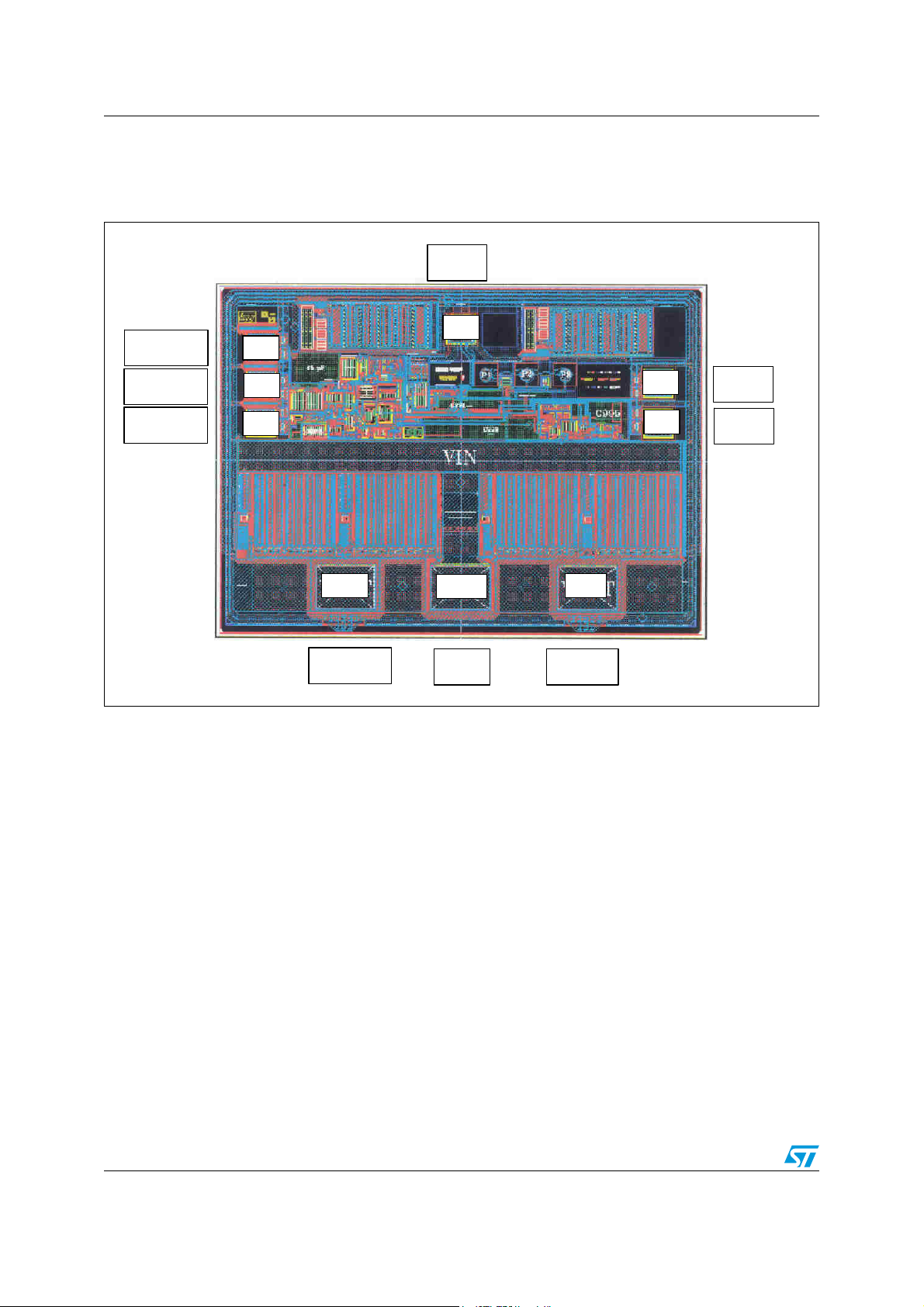
7 Die information
Figure 4. Die map
GND
0
1002
INBH
-1542
ADJ
-1545
SENSE
-1545
868
574
287
14
15
16
VO
-890
1-2
-974
13
3-4-5
VI
0
-974
VO
970
6-7
-974
Note: Pad numbers reflect terminal numbers when placed in case FLAT-16.
10
8
OCM
1517
Short
1517
5
2
12/20 Doc ID 10005 Rev 14

RHFL4913A Die information
7.1 Die bonding pad locations and electrical functions
Die physical dimensions:
Die size: 150 mils x 110 mils (3.81 mm by 2.79 mm)
Die thickness: 375 µm ± 25 µm (14.8 mils ± 1 mil)
Pad size: V
Control pads: 184 µm x 184 µm (7.25 mils square)
Interface materials:
Top metallization: Al/Si/Cu, 1.05 µm ± 0.15 µm
Backside metallization: none
Glassivation:
Type: p. vapox + nitride
Thickness: 0.6 µm ± 0.1 µm + 0.6 µm ± 0.08 µm
Substrate: bare silicon
Assembly related information:
Substrate potential: floating recommended to be tied to ground
Special assembly instructions: "Sense" pad not used; not internally connected to
any part of the IC. Can be connected to ground when space anti-static electricity
rules apply.
, V
IN
pads: 450 µm x 330 µm (17.7 mils by 13 mils)
OUT
Doc ID 10005 Rev 14 13/20

Package mechanical data RHFL4913A
8 Package mechanical data
In order to meet environmental requirements, ST offers these devices in different grades of
ECOPACK
specifications, grade definitions and product status are available at: www.st.com.
ECOPACK
®
packages, depending on their level of environmental compliance. ECOPACK®
®
is an ST trademark.
14/20 Doc ID 10005 Rev 14

RHFL4913A Package mechanical data
FLAT-16 (MIL-STD-1835) mechanical data
mm. inch.
Dim.
Min. Typ. Max. Min. Typ. Max.
A 2.16 2.72 0.085 0.107
b 0.43 0.017
c0.13 0.005
D 9.910.390
E6.91 0.272
E2 4.32 0.170
E3 0.76 0.030
e 1.27 0.050
L 6.72 0.265
Q 0.66 1.14 0.026 0.045
S1 0.13 0.005
e
L
16
E
1 8
L
b
9
c
E3
E2
E3
S1
D
Q
A
7450901A
Doc ID 10005 Rev 14 15/20

Package mechanical data RHFL4913A
SMD5C mechanical data
Dim.
A2.84 3.00 3.15 0.112 0.118 0.124
A1 0.25 0.38 0.51 0.010 0.015 0.020
b 7.13 7.26 7.39 0.281 0.286 0.291
b14.95 5.08 5.21 0.195 0.200 0.205
b2 2.28 2.41 2.54 0.090 0.095 0.100
b3 2.92 3.05 3.18 0.115 0.120 0.125
D13 .71 13.8413.97 0.540 0.545 0.550
D1 0.76 0.030
E7.39 7.52 7.65 0.291 0.2960.301
e1.91 0.075
Min. Typ. Max. Min. Typ. Max.
mm. inch.
16/20 Doc ID 10005 Rev 14
7924296B

RHFL4913A Packaging
9 Packaging
The RHFL4913A adjustable voltage regulator is available in a high thermal dissipation 16pin hermetic Flat package, the bottom flange of which is metallized to allow direct soldering
to a heat sink (efficient thermal conductivity). The device is also available in the SMD5C
hermetic ceramic package.
Doc ID 10005 Rev 14 17/20

Ordering information RHFL4913A
10 Ordering information
Table 5. Order codes
Die FLAT-16 SMD5C
RHFL4913KPA-01V RHFL49143SCA-07V Gold
RHFL4913KPA-02V Solder
RHFL4913KPA1 RHFL4913SCA1 Gold
RHFL4913KPA2 RHFL4913SCA2 Gold
L4913ADIE2V
L4913ADIES
Table 6. Part numbers - SMD equivalent
ST part number SMD part number
RHFL4913KPA-01V 5962F0252401VXC
RHFL4913KPA-02V 5962F0252401VXA
RHFL4913SCA-07V 5962F0252403VUC
L4913ADIE2V 5962F0252401V9A
Table 7. Environmental characteristics
Terminal
finish
Output
voltage
Adj
Adj
Adj
Adj
Adj
Adj
Quality level
QML-V
QML-V
EM1
EM2=EM1+48hours B.I.
QML-V die
EM1 die
Parameter Conditions Value Unit
Output voltage thermal drift -55°C to +125°C 40 ppm/°C
Output voltage radiation drift From 0 krad to 300 krad at 0.55 rad/s 8 ppm/krad
Output voltage radiation drift
From 0 krad to 300 krad, Mil Std 883E Method
1019.6
6 ppm/krad
18/20 Doc ID 10005 Rev 14

RHFL4913A Revision history
11 Revision history
Table 8. Document revision history
Date Revision Changes
29-Oct-2004 3 New order codes added - Tables 4 and 5.
27-May-2005 4
08-Jun-2005 5
30-Jan-2006 6 Added new package SMD5C and removed old package SOC-16.
26-Jan-2007 7 DIE Information and DIE Pad has been updated par. 6, pages 9 and 10.
23-Nov-2007 8
22-Sep-2008 9 Modified Application information on page 10.
17-Nov-2008 10 Modified Table 6 on page 18.
21-Jan-2010 11 Modified Table 5 on page 18.
18-Oct-2010 12 Modified Section 6.1 on page 10.
Features, Tables 4, 5 and the Figure 1 has been updated. Add the Mechanical
Data SOC-16.
Mistake on Table 4 (Q.ty Level), Table 7 has been updated and add DIE
Information.
Pin information for the SMD5C package updated in Ta bl e 1 ; added section 6.3:
FPGA power supply lines on page 11. Minor text changes.
07-Feb-2011 13 Added: note Table 1 on page 4.
07-Dec-2011 14 Removed the note under Table 1 on page 4 and added footnotes 1 and 2.
Doc ID 10005 Rev 14 19/20

RHFL4913A
Please Read Carefully:
Information in this document is provided solely in connection with ST products. STMicroelectronics NV and its subsidiaries (“ST”) reserve the
right to make changes, corrections, modifications or improvements, to this document, and the products and services described herein at any
time, without notice.
All ST products are sold pursuant to ST’s terms and conditions of sale.
Purchasers are solely responsible for the choice, selection and use of the ST products and services described herein, and ST assumes no
liability whatsoever relating to the choice, selection or use of the ST products and services described herein.
No license, express or implied, by estoppel or otherwise, to any intellectual property rights is granted under this document. If any part of this
document refers to any third party products or services it shall not be deemed a license grant by ST for the use of such third party products
or services, or any intellectual property contained therein or considered as a warranty covering the use in any manner whatsoever of such
third party products or services or any intellectual property contained therein.
UNLESS OTHERWISE SET FORTH IN ST’S TERMS AND CONDITIONS OF SALE ST DISCLAIMS ANY EXPRESS OR IMPLIED
WARRANTY WITH RESPECT TO THE USE AND/OR SALE OF ST PRODUCTS INCLUDING WITHOUT LIMITATION IMPLIED
WARRANTIES OF MERCHANTABILITY, FITNESS FOR A PARTICULAR PURPOSE (AND THEIR EQUIVALENTS UNDER THE LAWS
OF ANY JURISDICTION), OR INFRINGEMENT OF ANY PATENT, COPYRIGHT OR OTHER INTELLECTUAL PROPERTY RIGHT.
UNLESS EXPRESSLY APPROVED IN WRITING BY TWO AUTHORIZED ST REPRESENTATIVES, ST PRODUCTS ARE NOT
RECOMMENDED, AUTHORIZED OR WARRANTED FOR USE IN MILITARY, AIR CRAFT, SPACE, LIFE SAVING, OR LIFE SUSTAINING
APPLICATIONS, NOR IN PRODUCTS OR SYSTEMS WHERE FAILURE OR MALFUNCTION MAY RESULT IN PERSONAL INJURY,
DEATH, OR SEVERE PROPERTY OR ENVIRONMENTAL DAMAGE. ST PRODUCTS WHICH ARE NOT SPECIFIED AS "AUTOMOTIVE
GRADE" MAY ONLY BE USED IN AUTOMOTIVE APPLICATIONS AT USER’S OWN RISK.
Resale of ST products with provisions different from the statements and/or technical features set forth in this document shall immediately void
any warranty granted by ST for the ST product or service described herein and shall not create or extend in any manner whatsoever, any
liability of ST.
ST and the ST logo are trademarks or registered trademarks of ST in various countries.
Information in this document supersedes and replaces all information previously supplied.
The ST logo is a registered trademark of STMicroelectronics. All other names are the property of their respective owners.
© 2011 STMicroelectronics - All rights reserved
STMicroelectronics group of companies
Australia - Belgium - Brazil - Canada - China - Czech Republic - Finland - France - Germany - Hong Kong - India - Israel - Italy - Japan -
Malaysia - Malta - Morocco - Philippines - Singapore - Spain - Sweden - Switzerland - United Kingdom - United States of America
www.st.com
20/20 Doc ID 10005 Rev 14
 Loading...