

Page 1

8 keys with individual key state outputs or I2C interface
LQFP32 (7x7 mm)
Features
■ Patented charge-transfer design
■ Up to 8 independent QTouch™ keys supported
■ Individual key state outputs or I
■ Fully “debounced” results
■ Patented AKS™ Adjacent Key Suppression
■ Self-calibration and auto drift compensation
■ Spread-spectrum bursts to reduce EMI
■ Up to 5 general-purpose outputs
■ ECOPACK® (RoHS compliant) package
Applications
This device specifically targets human interfaces
and front panels for a wide range of applications
such as PC peripherals, home entertainment
systems, gaming devices, lighting and appliance
controls, remote controls, etc.
QST devices are designed to replace mechanical
switching/control devices and the reduced
number of moving parts in the end product
provides the following advantages:
■ Lower customer service costs
■ Reduced manufacturing costs
■ Increased product lifetime
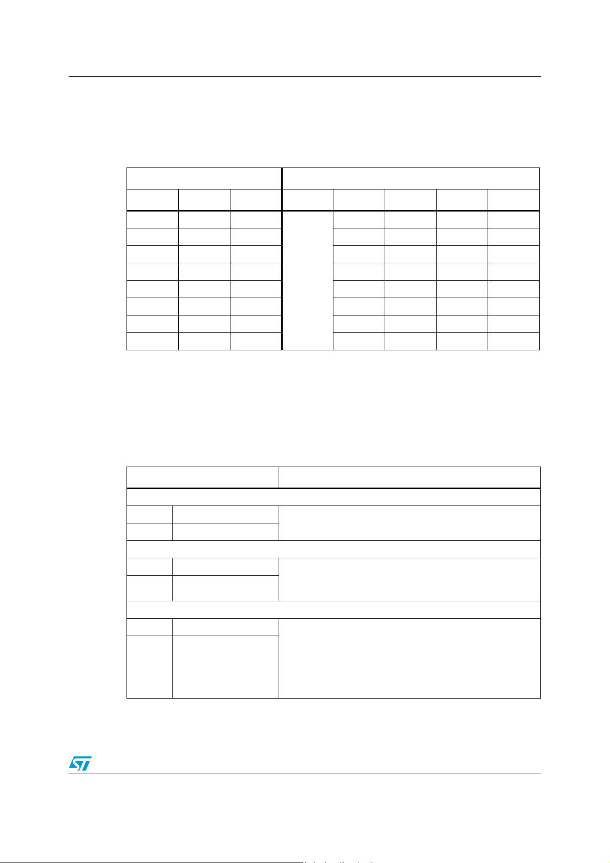
Table 1. Device summary
2
C interface
QST108
Capacitive touch sensor device
Not For New Design
Description
The QST108 is the ideal solution for the design of
capacitive touch sensing user interfaces.
Touch-sensitive controls are increasingly
replacing electromechanical switches in home
appliances, consumer and mobile electronics,
and in computers and peripherals. Capacitive
touch controls allow designers to create stylish,
functional, and economical designs which are
highly valued by consumers, often at lower cost
than the electromechanical solutions they
replace.
The QST108 QTouch™ sensor IC is a pure digital
solution based on Quantum's patented chargetransfer (QProx™) capacitive technology.
QTouch™ and QProx™ are trademarks of the
Quantum Research Group.
Order codes
Feature
QST108KT6
Operating supply voltage 2.4 to 5.5 V
Supported interfaces Individual key state outputs or I
Operating temperature -40° to +85° C
Package LQFP32 (7x7 mm)
July 2008 Rev 5 1/51
This is information on a product still in production but not recommended for new designs.
2
C Interface
www.st.com
1
Page 2

Contents QST108
Contents
1 Device overview . . . . . . . . . . . . . . . . . . . . . . . . . . . . . . . . . . . . . . . . . . . . 5
2 Pin description . . . . . . . . . . . . . . . . . . . . . . . . . . . . . . . . . . . . . . . . . . . . . 6
3 QST touch sensing technology . . . . . . . . . . . . . . . . . . . . . . . . . . . . . . . . 8
3.1 Functional description . . . . . . . . . . . . . . . . . . . . . . . . . . . . . . . . . . . . . . . . 8
3.2 Spread-spectrum operation . . . . . . . . . . . . . . . . . . . . . . . . . . . . . . . . . . . . 8
3.3 Faulty and unused keys . . . . . . . . . . . . . . . . . . . . . . . . . . . . . . . . . . . . . . . 9
3.4 Detection threshold levels . . . . . . . . . . . . . . . . . . . . . . . . . . . . . . . . . . . . . 9
3.5 Detection integrator filter . . . . . . . . . . . . . . . . . . . . . . . . . . . . . . . . . . . . . . 9
3.6 Self-calibration . . . . . . . . . . . . . . . . . . . . . . . . . . . . . . . . . . . . . . . . . . . . . 10
3.7 Fast positive recalibration . . . . . . . . . . . . . . . . . . . . . . . . . . . . . . . . . . . . . 10
3.8 Forced key recalibration . . . . . . . . . . . . . . . . . . . . . . . . . . . . . . . . . . . . . . 10
3.9 Max On-Duration . . . . . . . . . . . . . . . . . . . . . . . . . . . . . . . . . . . . . . . . . . . 11
3.10 Drift compensation . . . . . . . . . . . . . . . . . . . . . . . . . . . . . . . . . . . . . . . . . . 11
3.11 Adjacent key suppression (AKS™) . . . . . . . . . . . . . . . . . . . . . . . . . . . . . 12
4 Device operating modes . . . . . . . . . . . . . . . . . . . . . . . . . . . . . . . . . . . . . 13
4.1 Reset and power-up . . . . . . . . . . . . . . . . . . . . . . . . . . . . . . . . . . . . . . . . . 13
4.2 Burst operation . . . . . . . . . . . . . . . . . . . . . . . . . . . . . . . . . . . . . . . . . . . . . 13
4.3 Low power mode . . . . . . . . . . . . . . . . . . . . . . . . . . . . . . . . . . . . . . . . . . . 13
4.4 Mode selection . . . . . . . . . . . . . . . . . . . . . . . . . . . . . . . . . . . . . . . . . . . . . 14
4.5 Stand-alone mode . . . . . . . . . . . . . . . . . . . . . . . . . . . . . . . . . . . . . . . . . . 15
4.5.1 Main features . . . . . . . . . . . . . . . . . . . . . . . . . . . . . . . . . . . . . . . . . . . . . 15
4.5.2 KOUT outputs . . . . . . . . . . . . . . . . . . . . . . . . . . . . . . . . . . . . . . . . . . . . 16
4.5.3 Option descriptions . . . . . . . . . . . . . . . . . . . . . . . . . . . . . . . . . . . . . . . . 17
4.6 I2C mode . . . . . . . . . . . . . . . . . . . . . . . . . . . . . . . . . . . . . . . . . . . . . . . . . 19
4.6.1 Main features . . . . . . . . . . . . . . . . . . . . . . . . . . . . . . . . . . . . . . . . . . . . . 19
4.6.2 General-purpose outputs . . . . . . . . . . . . . . . . . . . . . . . . . . . . . . . . . . . . 20
4.6.3 IRQ pin . . . . . . . . . . . . . . . . . . . . . . . . . . . . . . . . . . . . . . . . . . . . . . . . . . 20
4.6.4 Communication packet . . . . . . . . . . . . . . . . . . . . . . . . . . . . . . . . . . . . . 20
4.6.5 I2C address selection . . . . . . . . . . . . . . . . . . . . . . . . . . . . . . . . . . . . . . 21
4.7 Supported commands . . . . . . . . . . . . . . . . . . . . . . . . . . . . . . . . . . . . . . . 21
2/51
Page 3

QST108 Contents
5 Design guidelines . . . . . . . . . . . . . . . . . . . . . . . . . . . . . . . . . . . . . . . . . . 27
5.1 CS sense capacitor . . . . . . . . . . . . . . . . . . . . . . . . . . . . . . . . . . . . . . . . . . 27
5.2 Sensitivity tuning . . . . . . . . . . . . . . . . . . . . . . . . . . . . . . . . . . . . . . . . . . . 27
5.2.1 Increasing sensitivity . . . . . . . . . . . . . . . . . . . . . . . . . . . . . . . . . . . . . . . 27
5.2.2 Decreasing sensitivity . . . . . . . . . . . . . . . . . . . . . . . . . . . . . . . . . . . . . . 27
5.2.3 Key balance . . . . . . . . . . . . . . . . . . . . . . . . . . . . . . . . . . . . . . . . . . . . . . 27
5.3 Power supply . . . . . . . . . . . . . . . . . . . . . . . . . . . . . . . . . . . . . . . . . . . . . . 28
5.4 ESD protection . . . . . . . . . . . . . . . . . . . . . . . . . . . . . . . . . . . . . . . . . . . . . 28
5.5 Crosstalk precautions . . . . . . . . . . . . . . . . . . . . . . . . . . . . . . . . . . . . . . . . 28
5.6 PCB layout and construction . . . . . . . . . . . . . . . . . . . . . . . . . . . . . . . . . . 28
6 Electrical characteristics . . . . . . . . . . . . . . . . . . . . . . . . . . . . . . . . . . . . 30
6.1 Parameter conditions . . . . . . . . . . . . . . . . . . . . . . . . . . . . . . . . . . . . . . . . 30
6.1.1 Minimum and maximum values . . . . . . . . . . . . . . . . . . . . . . . . . . . . . . . 30
6.1.2 Typical values . . . . . . . . . . . . . . . . . . . . . . . . . . . . . . . . . . . . . . . . . . . . . 30
6.1.3 Typical curves . . . . . . . . . . . . . . . . . . . . . . . . . . . . . . . . . . . . . . . . . . . . 30
6.1.4 Loading capacitor . . . . . . . . . . . . . . . . . . . . . . . . . . . . . . . . . . . . . . . . . 30
6.1.5 Pin input voltage . . . . . . . . . . . . . . . . . . . . . . . . . . . . . . . . . . . . . . . . . . 30
6.2 Absolute maximum ratings . . . . . . . . . . . . . . . . . . . . . . . . . . . . . . . . . . . . 31
6.3 EMC characteristics . . . . . . . . . . . . . . . . . . . . . . . . . . . . . . . . . . . . . . . . . 32
6.3.1 Functional EMS (electro magnetic susceptibility) . . . . . . . . . . . . . . . . . 32
6.3.2 Electro magnetic interference (EMI) . . . . . . . . . . . . . . . . . . . . . . . . . . . 32
6.3.3 Absolute maximum ratings (electrical sensitivity) . . . . . . . . . . . . . . . . . 33
6.4 Operating conditions . . . . . . . . . . . . . . . . . . . . . . . . . . . . . . . . . . . . . . . . 34
6.5 Supply current characteristics . . . . . . . . . . . . . . . . . . . . . . . . . . . . . . . . . 34
6.6 Capacitive sensing characteristics . . . . . . . . . . . . . . . . . . . . . . . . . . . . . . 35
6.7 KOUTn/OPTn/GPOn pin characteristics . . . . . . . . . . . . . . . . . . . . . . . . . 36
6.7.1 General characteristics . . . . . . . . . . . . . . . . . . . . . . . . . . . . . . . . . . . . . 36
6.7.2 Output pin characteristics . . . . . . . . . . . . . . . . . . . . . . . . . . . . . . . . . . . 36
6.8 RESET pin . . . . . . . . . . . . . . . . . . . . . . . . . . . . . . . . . . . . . . . . . . . . . . . . 39
6.9 I2C control interface . . . . . . . . . . . . . . . . . . . . . . . . . . . . . . . . . . . . . . . . . 40
7 Package mechanical data . . . . . . . . . . . . . . . . . . . . . . . . . . . . . . . . . . . . 42
7.1 Soldering information . . . . . . . . . . . . . . . . . . . . . . . . . . . . . . . . . . . . . . . . 45
8 Part numbering . . . . . . . . . . . . . . . . . . . . . . . . . . . . . . . . . . . . . . . . . . . . 46
9 Device revision information . . . . . . . . . . . . . . . . . . . . . . . . . . . . . . . . . . 47
3/51
Page 4

Contents QST108
9.1 Device revision identification . . . . . . . . . . . . . . . . . . . . . . . . . . . . . . . . . . 47
9.2 Device revision history . . . . . . . . . . . . . . . . . . . . . . . . . . . . . . . . . . . . . . . 47
9.2.1 Revision 2.1 . . . . . . . . . . . . . . . . . . . . . . . . . . . . . . . . . . . . . . . . . . . . . . 47
9.2.2 Revision 2.3 . . . . . . . . . . . . . . . . . . . . . . . . . . . . . . . . . . . . . . . . . . . . . . 48
10 Revision history . . . . . . . . . . . . . . . . . . . . . . . . . . . . . . . . . . . . . . . . . . . 49
4/51
Page 5

QST108 Device overview
1 Device overview
The QST108 capacitive touch sensor IC is a pure digital solution based on Quantum's
patented charge-transfer (QProx™) capacitive technology.
This technology allows users to create simple touch panel sensing electrode interfaces for
conventional or flexible printed circuit boards (PCB/FPCB). Sensing electrodes are part of
the PCB layout (copper pattern or printed conductive ink) and may be used in various
shapes (circle, rectangular, etc.).
By implementing the QProx™ charge-transfer algorithm, the QST108 detects finger
presence (human touch) near electrodes behind a dielectric (glass, plastic, wood, etc.). Only
one external sampling capacitor by channel is used in the measuring circuitry to control the
detection.
QST technology also incorporates advanced processing techniques such as drift
compensation, auto-calibration, noise filtering, and Quantum's patented Adjacent Key
Suppression™ (AKS™) to ensure maximum usability and control integrity.
In order to meet environmental requirements, ST offers this device in ECOPACK®
packages. These packages have a lead-free second level interconnect. The category of
second level interconnect is marked on the package and on the inner box label, in
compliance with JEDEC Standard JESD97.
The maximum ratings related to soldering conditions are also marked on the inner box label.
ECOPACK is an ST trademark. ECOPACK specifications are available at: www.st.com.
5/51
Page 6

Pin description QST108
SNS_SCK1
32 31 30 29 28 27 26 25
24
23
22
21
20
19
18
17
9 101112131415
16
1
2
3
4
5
6
7
8
I2C_SCL/KOUT81) (HS)
RESET
NC
V
DD_1
GPO4/KOUT4/OPT4 (HS)
GPO5/KOUT5/OPT5 (HS)
IRQ/KOUT6/OPT6 (HS)
I2C_SDA/KOUT71) (HS)
V
SS_2VSS_3VSS_4
V
DD_2
SNSK_SCK1
SNS_SCK2
V
SS_1
SNS_SCK6
SNSK_SCK5
SNSK_SCK2
SNS_SCK3
SNS_SCK4
SNS_SCK5
SNSK_SCK4
SNSK_SCK3
SNS_SCK8
SNSK_SCK7
SNS_SCK7
SNSK_SCK6
GPO3/OPT3/KOUT3 (HS)
GPO2/OPT2/KOUT2 (HS)
GPO1/OPT1/KOUT1 (HS)
SNSK_SCK8
QST108KT6
(HS) 20 mA high sink capability (on N-buffer only)
2 Pin description
Figure 1. 32-pin package pinout
Table 2. Device pin description
Pin Pin name Type
1 GPO4/OPT4/KOUT4
2 GPO5/OPT5/KOUT5
3 OPT6/KOUT6/IRQ
4 KOUT7/I2C_SDA
5 KOUT8/I2C_SCL
6/51
1. An external pull-up is required on these pins.
(1)
Stand-alone mode function I2C mode function If unused
(2)
PP (HS)
(2)
PP (HS)
(2)
(3)
(3)
PP/OD
(HS)
TOD
(HS)
TOD
(HS)
Key 4 output / BCD output 4
and MOD_0 option resistor
Key 5 output and
MOD_1 option resistor
Key 6 output and
OM_0 option resistor
Key 7 output I
Key 8 output I
General purpose output 4
and I²C address bit 2
option resistor
Option
resistor
Open or
General purpose output 5
option
resistor
Open or
Interrupt line (active low)
option
resistor
2
C serial data Open
2
C serial clock Open
Page 7

QST108 Pin description
Table 2. Device pin description (continued)
Pin Pin name Type
6 RESET
7 NC Not connected
(1)
Stand-alone mode function I2C mode function If unused
BD Reset (active low)
10nF
capacitor to
ground
8V
9V
10 V
11 V
12 V
13 V
DD_1
SS_1
SS_2
SS_3
SS_4
DD_2
S Supply voltage
S Ground voltage
S Ground voltage
S Ground voltage
S Ground voltage
S Supply voltage
14 SNS_SCK1 SNS Key 1 sense pin to Cs Open
15 SNSK_SCK1 SNS Key 1 sense pin to Cs/Rs Open
16 SNS_SCK2 SNS Key 2 sense pin to Cs Open
17 SNSK_SCK2 SNS Key 2 sense pin to Cs/Rs Open
18 SNS_SCK3 SNS Key 3 sense pin to Cs Open
19 SNSK_SCK3 SNS Key 3 sense pin to Cs/Rs Open
20 SNS_SCK4 SNS Key 4 sense pin to Cs Open
21 SNSK_SCK4 SNS Key 4 sense pin to Cs/Rs Open
22 SNS_SCK5 SNS Key 5 sense pin to Cs Open
23 SNSK_SCK5 SNS Key 5 sense pin to Cs/Rs Open
24 SNS_SCK6 SNS Key 6 sense pin to Cs Open
25 SNSK_SCK6 SNS Key 6 sense pin to Cs/Rs Open
26 SNS_SCK7 SNS Key 7 sense pin to Cs Open
27 SNSK_SCK7 SNS Key 7 sense pin to Cs/Rs Open
28 SNS_SCK8 SNS Key 8 sense pin to Cs Open
29 SNSK_SCK8 SNS Key 8 sense pin to Cs/Rs Open
(2)
(2)
(2)
PP (HS)
PP (HS)
PP (HS)
30 GPO1/OPT1/KOUT1
31 GPO2/OPT2/KOUT2
32 GPO3/OPT3/KOUT3
1. S: supply pin, BD: bidirectional pin, SNS: capacitive sensing pin, PP: Output push-pull, OD: Output open-drain,
TOD: Output true open-drain and HS: 20mA high sink capability (on N-buffer only)
2. During the reset phase, these pins are floating and their state depends on the option resistor.
3. An external pull-up is required on these pins.
Key 1 output / BCD output 1
and MODE option resistor
Key 2 output / BCD output 2
and AKS option resistor
Key 3 output / BCD output 3
and LP option resistor
General purpose output 1
and MODE option resistor
General purpose output 2
and I2C address bit 0
option resistor
General purpose output 3
and I2C address bit 1
option resistor
Option
resistor
Option
resistor
Option
resistor
7/51
Page 8

QST touch sensing technology QST108
Ai12569
SNS_SCKn
SNSK_SCKn
Sense capacitor
C
S
(a few nF)
Cx (~20 pF)
CT (~5 pF)
Earth
Serial resistor
R
S
(10 kΩ)
3 QST touch sensing technology
3.1 Functional description
QST devices employ bursts of charge-transfer cycles to acquire signals. Burst mode permits
low power operation, dramatically reduces RF emissions, lowers susceptibility to RF fields,
and yet permits excellent speed. Signals are processed using algorithms pioneered by
Quantum which are specifically designed to provide reliable, trouble-free operation over the
life of the product.
The QST switches and charge measurement hardware functions are all internal to the
device. An external C
then measured. Larger values of C
rapidly, reducing available resolution. As a minimum resolution is required for proper
operation, this can result in dramatically reduced gain. Larger values of C
of differential voltage across it, increasing available resolution by permitting longer QST
bursts. The value of C
The device is responsive to both C
changes in sensor gain.
Figure 2. QTouch™ measuring circuitry
capacitor accumulates the charge from sense-plate CX, which is
S
can thus be increased to allow larger values of CX to be tolerated.
S
cause the charge transferred into CS to rise more
X
reduce the rise
S
and CS, and changes in either can result in substantial
X
3.2 Spread-spectrum operation
The bursts operate over a spread of frequencies, so that external fields will have minimal
effect on key operation and emissions are very weak. Spread-spectrum operation works
with the Detection Integrator mechanism (DI) to dramatically reduce the probability of false
detection due to noise.
8/51
Page 9

QST108 QST touch sensing technology
3.3 Faulty and unused keys
Any sensing channel that does not have its sense capacitor (CS) fitted is assumed to be
either faulty or unused. This channel takes no further part in operation unless a Mastercommanded recalibration operation shows it to have an in-range burst count again. Faulty,
unused or disabled keys are still bursted but not processed to avoid modifying the sensitivity
of active keys.
This is important for sensing channels that have an open or short circuit fault across C
Such channels would otherwise cause very long acquire bursts, and in consequence would
slow the operation of the entire QST device.
To optimize touch response time and device power consumption, if some keys are not used,
we recommend to try suppressing the ones which belong to the same burst. Bursts which
do not have any keys implemented will then not be processed.
3.4 Detection threshold levels
The key capacitance change induced by the presence of a finger is sensed by the variation
in the number of charge transfer pulses to load the capacitor. The difference in the pulse
count number is compared to a threshold in order to detect the key as pressed or not.
Two different thresholds, one for detection and one for the end of detection, create an
hysteresis in order to prevent erratic behavior.
The default threshold levels and hysteresis values are described in Section 6.6: Capacitive
sensing characteristics on page 35.
3.5 Detection integrator filter
The Detection Integrator (DI) filter mechanism works together with spread spectrum
operation to dramatically reduce the effects of noise on key states. The DI mechanism
requires a specified number of measurements that qualify as detections (and these must
occur in a row) or the detection will not be reported.
.
S
In a similar manner, the end of a touch (loss of signal) also has to be confirmed over several
measurements. It is called the End of Detection Integrator (EDI).
This process acts as a type of “debounce” mechanism against noise.
The default DI and EDI values for confirming start of touch and end of touch are described in
Section 6.6: Capacitive sensing characteristics on page 35.
9/51
Page 10

QST touch sensing technology QST108
Burst count
Time
Reference count
Reference + EofDeTh
Reference + DeThHysteresis
Key Detection signal
= Sampling point
Figure 3 shows an example of detection with DI=2 and EDI=2 meaning 3 consecutive
samples are necessary to trigger the key detection or end of detection
Figure 3. Detection signals
3.6 Self-calibration
On power-up, all keys are self-calibrated to provide reliable operation under almost any
conditions. The calibration phase is used to compute a reference value per key which is then
used by the process determining if a key is touched or not. The reference is an average of 8
single acquisitions. As a result, the calibration time of the system can be simply calculated
using the following formula: t
= 8 * Burst_Period. The methodology used to measure the
CAL
burst period is described in application note AN2547. For a maximum calibration duration
(t
), please refer to Section 6.6: Capacitive sensing characteristics on page 35.
CAL
3.7 Fast positive recalibration
The device autorecalibrates a key when its signal reflects a decrease in capacitance higher
than a fixed threshold (PosRecalTh) for a defined number of acquisitions (PosRecalI).
3.8 Forced key recalibration
A recalibration of the device may be issued at any time by sending to the QST device the
appropriate I
It is possible to recalibrate independently any individual key using an I
2
C command or by tying the RESET pin to ground.
2
C command.
10/51
Page 11

QST108 QST touch sensing technology
3.9 Max On-Duration
The device can time out and automatically recalibrate each key independently after a fixed
duration of continuous touch detection. This prevents the keys from becoming ‘stuck on’ due
to foreign objects or other sudden influences. This is known as the Max On-Duration feature.
After recalibration, the key will continue to operate normally, even if partially or fully
obstructed. Max On-Duration works independently per channel: a timeout on one channel
has no effect on another channel.
Infinite timeout is useful in applications where a prolonged detection can occur and where
the output must reflect the detection no matter how long. In infinite timeout mode, the
designer should take care to ensure that drift in C
remain “stuck on” inadvertently even when the touching object is removed from the sense
field. Timeout durations are not accurate and can vary substantially depending on V
temperature values, and should not be relied upon for critical functions.
, CX, and VDD do not cause the device to
S
and
DD
3.10 Drift compensation
Signal drift can occur because of changes in CX, CS, and VDD over time. Depending on the
C
type and quality, the signal may vary substantially with temperature and veiling. If keys
S
are subject to extremes of temperature or humidity, the signal can also drift. It is crucial that
drift be compensated, otherwise false detections, non detections, and sensitivity shifts will
follow.
Drift compensation slowly corrects the reference level of each key while no detection is in
effect. The rate of reference adjustment must be performed slowly or else legitimate
detections can also be ignored. The device compensates drift on each channel
independently using a maximum compensation rate to the reference level.
Once a touch is sensed, the drift compensation mechanism ceases since the signal is
legitimately high, and therefore should not cause the reference level to change.
The signal drift compensation is “asymmetric”: the reference level compensates drift in one
direction faster than it does in the other. Specifically, it compensates faster for increasing
signals than for decreasing signals. Decreasing signals should not be compensated for
quickly, since an approaching finger could be compensated for partially or entirely while
approaching the sense electrode. However, an obstruction over the sense pad, for which the
sensor has already made full allowance, could suddenly be removed leaving the sensor with
an artificially elevated reference level and thus become insensitive to touch. In this latter
case, the sensor will compensate for the object's removal very quickly, usually in only a few
seconds.
Caution: When only one key is enabled or if keys are very close together, the common drift
compensation must be disabled or its rate must be reduced to ensure correct device
operation.
11/51
Page 12

QST touch sensing technology QST108
Burst count
Reference + DeTh
Reference Count
Reference Count + PosRelTh
Time
Drift Compensation
Temperature Change
Figure 4 illustrates an example of the drift compensation algorithm following a temperature
change.
Figure 4. Drift compensation example
3.11 Adjacent key suppression (AKS™)
Adjacent key suppression (AKS™) is a Quantum-patented feature which prevents multiple
keys from responding to a single touch. This can happen with closely spaced keys, or a
scroll wheel that has buttons very near it.
The QST108 supports two AKS modes:
● Locking AKS
Once a key is considered as “touched”, all other keys are locked in an untouched state.
To unlock these keys, the touched key must return to an untouched state. Then, the key
having the lowest key ID number is declared as the “touched” one.
● Unlocking AKS
On each acquisition, the signal strengths from each key are compared and the key with
the highest signal level is declared as the “touched” one.
2
In I
C mode, up to 8 AKS groups can be specified.
Note: All keys belonging to the same AKS group must have the same AKS mode.
12/51
Page 13

QST108 Device operating modes
4 Device operating modes
4.1 Reset and power-up
At power-up, the device configures itself according to the pull-up or pull-down option
resistors present on pins OPT1 to OPT6. The device start-up and configuration may take up
to t
When the power is established, it is possible to force a new device configuration by applying
a negative pulse on the RESET
Setup
.
pin.
The RESET
device resets itself (through an I²C command, for example).
A 10nF capacitor is recommended on the RESET
immunity.
pin is a bidirectional pin with an internal pull-up. The line is forced low when the
4.2 Burst operation
The device operates in “Burst” mode. Each key touch is acquired using a burst of chargetransfer sensing pulses whose count varies depending on the value of the sense capacitor
C
and the load capacitance CX. Key touches are acquired using two successive bursts of
S
pulses:
● Burst A: Keys 1, 2, 3, and 4
● Burst B: Keys 5, 6, 7, and 8
Bursts always operate in an A-B sequence. If Keys 5 to 8 are not implemented, the QST
device will not perform the Burst B to improve the response time and reduce the power
consumption when in Low Power (LP) mode.
In Low Power mode, the device sleeps in an ultra-low current state between bursts to
conserve power.
4.3 Low power mode
pin to ensure reliable start-up and noise
In order to reduce the device power consumption, the QST family include scalable low
power modes.
● Standard low power mode
When the device is in standard low power mode, a window with very low power
consumption is inserted between the acquisition of the last active key and the following
acquisition of the first active key.
This window duration is programmable as the 'sleep duration time'.
Note that the sleep window insertion is cancelled in the following conditions:
– If a change is detected on a key, in order to speed up the DI process, the sleep
window insertion is skipped until the end of the DI process.
–In I
– Inside an I
2
C mode, when a key change is actually detected and reported with a negative
pulse on the IRQ
command is received from the host.
2
period is skipped.
pin. In this case, the low power mode is disabled until a
C command, between the Write and the Read I2C frames, the sleep
13/51
Page 14

Device operating modes QST108
● Free run in detect
The behavior in this mode is the same as in the standard low power mode except that
the sleep window insertion is always skipped if any of the active keys is detected as
touched.
This is useful to improve the wheel response time.
● Deep Sleep mode
Caution: If an I
does not acknowledge the frame (even if it has an I
In Deep Sleep mode, the device enters a very low power mode indefinitely. The device
resumes its operations after receiving an I
2
C frame is received while in Sleep or Deep Sleep mode, the device wakes up but
2
C frame with any address or a reset.
2
C frame with the device address). The
host must therefore send again the frame until it is taken in account and acknowledged.
4.4 Mode selection
The device options are configured by connecting pull-up or pull-down resistors on OPTn
pins. The device operating mode is selected using option pin 1 (OPT1) while the device
settings are configured using option pins OPT2 to OPT6 (Tab le 3 ). Option pins are sampled
at power-up and after a reset.
To fit most applications, the QST108 device offers two different operating modes:
● Stand-alone mode
This mode allows the user to simply replace existing mechanical switches with a
capacitive sensing solution. It is designed for maximum flexibility and can
accommodate most popular sensing requirements via option resistors (AKS, Low
power, Max On-Duration and output modes).
In this mode, the 8 output pins reflect the status of the 8 sensing channels.
2
● I
C mode
In this mode, which is the most open one, the device is driven using the I
To avoid polling, the QST device features an output interrupt pin (IRQ
reports all key changes to the Master device. The QST (Slave) device can drive up to
five general-purpose outputs.
Table 3. Operating modes
2
C interface.
). The IRQ line
OPT1: Mode selection
Pin OPT1 is high at start-up Stand-alone mode AKS LP MOD_0 MOD_1 OM
Pin OPT1 is low at start-up I
14/51
2
C mode ADD0 ADD1 ADD2 Unused Unused
Option resistor function
OPT2 OPT3 OPT4 OPT5 OPT6
Page 15

QST108 Device operating modes
4.5 Stand-alone mode
This mode allows the user to simply replace existing mechanical switch interface with a
capacitive sensing solution. It is designed for maximum flexibility and can accommodate
most popular sensing requirements via option resistors (see Figure 5).
4.5.1 Main features
● Pins KOUT1 to KOUT8 directly reflect the state of keys
● Selectable global adjacent key suppression (AKS™)
● Selectable sleep duration
● Selectable Max On-Duration values
● Selectable BCD mode
15/51
Page 16

Ai12560
MOD_1/KOUT5
MOD_0/KOUT4
LP/KOUT3
AKS/KOUT2
V
SS_1
V
SS_2
V
SS_3
V
SS_4
V
DD_1
V
DD_2
RESET
V
UNREG
4.7µF 4.7µF
2.4~5.5V
Volt. Reg.
OM/KOUT6
KOUT7
KOUT8
MODE/KOUT1
V
DD
Binarycoded
Output
Mode
10nF
V
DD
10kΩ 10kΩ
To Host
100nF 100nF
SNS_SCK1
SNSK_SCK1
Key1
R
S1
10kΩ
C
S1
Keep these parts close to IC
SNS_SCK2
SNSK_SCK2
Key2
R
S2
10kΩ
C
S2
SNS_SCK3
SNSK_SCK3
Key3
R
S3
10kΩ
C
S3
SNS_SCK4
SNSK_SCK4
Key4
R
S4
10kΩ
C
S4
SNS_SCK5
SNSK_SCK5
Key5
R
S5
10kΩ
C
S5
SNS_SCK6
SNSK_SCK6
Key6
R
S6
10kΩ
C
S6
SNS_SCK7
SNSK_SCK7
Key7
R
S7
10kΩ
C
S7
SNS_SCK8
SNSK_SCK8
Key8
R
S8
10kΩ
C
S8
1
2
3
4
5
6
8
9 101112
13
14
15
16
17
18
19
20
21
22
23
24
25
26
27
28
29
30
31
32
1MΩ
V
DD
V
SS
KOUT6
1MΩ
V
DD
V
SS
KOUT5
1MΩ
V
DD
V
SS
KOUT4
1MΩ
V
DD
V
SS
KOUT3
1MΩ
V
DD
V
SS
KOUT2
1MΩ
V
DD
KOUT1
V
DD
KOUT8
KOUT7
Device operating modes QST108
Figure 5. Stand-alone mode typical schematic
4.5.2 KOUT outputs
16/51
KOUTn outputs directly reflect the state of keys. These pins are push-pull outputs except for
pins KOUT7 and KOUT8 which are true open-drain outputs. Under RESET, these pins are
floating and their state depends on the option resistors. Pins KOUTn are active high
meaning that when a key is “touched”, the corresponding KOUT pin outputs a ‘1’.
Page 17

QST108 Device operating modes
4.5.3 Option descriptions
Adjacent key suppression (AKS™)
The QST108 features an adjacent key suppression (AKS™) function.
This function is enabled using the AKS option resistor (OPT2) in standard output mode as
described in Ta bl e 4 . In BCD output mode, the AKS function is always enabled, regardless
of the option resistor configuration.
Table 4. AKS truth table
OPT2/AKS Description
V
SS
V
DD
Disabled
Global locking AKS on all available keys
Low Power mode option
This option resistor (OPT3) selects whether the device is always sensing the keys or if a low
power consumption phase is introduced between bursts as described in Tabl e 5 .
In Low Power mode, a very low consumption (sleep) phase of 100ms is inserted between
the Group B burst and the Group A burst. This significantly reduces the overall consumption
of the device. Sleep duration is not accurate and can vary substantially depending on V
and temperature values.
Note: In Low Power mode, the response time is increased.
Table 5. Low power (LP) mode truth table
OPT3/LP Description
V
SS
V
DD
Free running mode
100ms sleep duration
Max On-Duration
There are four recalibration timing options (“Max On-Duration”). The recalibration option
resistors (OPT4 and OPT5) control how long it takes for a continuous detection to trigger a
recalibration on a key as described in Tab le 6 . When such an event occurs, only the “stuck”
key is recalibrated.
Table 6. Max On-Duration (MOD) truth table
DD
OPT4/MOD_0 OPT5/MOD_1 Description
V
SS
V
SS
V
DD
V
DD
V
SS
V
DD
V
SS
V
DD
Infinite
60s
20s
10s
17/51
Page 18

Device operating modes QST108
Output mode option
The QST108 offers several outputs mode to fit any existing application.
Table 7. Output mode (OM) truth table
OPT6/OM Description
V
SS
V
DD
1. In BCD mode, the AKS function must be enabled.
Table 8. Binary code truth table
Individual key state output mode: One output per sensing channel
BCD output mode: Binary-coded touched key number (see Ta b le 8 )
KOUT4 KOUT3 KOUT2 KOUT1 Description
0 0 0 0 All released
0 0 0 1 Key 1 pressed
0 0 1 0 Key 2 pressed
0 0 1 1 Key 3 pressed
0 1 0 0 Key 4 pressed
0 1 0 1 Key 5 pressed
0 1 1 0 Key 6 pressed
0 1 1 1 Key 7 pressed
1 0 0 0 Key 8 pressed
Other Not used
(1)
18/51
Page 19

QST108 Device operating modes
Ai12559
I2C_SCL
I2C_SDA
GPO5
ADD2/GPO4
ADD1/GPO3
ADD0/GPO2
MODE/GPO1
V
SS_1VSS_2VSS_3VSS_4
SNS_SCK1
SNSK_SCK1
V
DD_1VDD_2
RESET
IRQ
Key1
SNS_SCK8
SNSK_SCK8
Key8
SNS_SCK7
SNSK_SCK7
Key7
V
DD
To
Host
MCU
R
S8
R
S7
R
S1
10kΩ
10kΩ
10kΩ
C
S8
C
S7
C
S1
SNS_SCK2
SNSK_SCK2
Key2
R
S2
10kΩ
C
S2
SNS_SCK3
SNSK_SCK3
Key3
R
S3
10kΩ
C
S3
SNS_SCK4
SNSK_SCK4
Key4
R
S4
10kΩ
C
S4
SNS_SCK5
SNSK_SCK5
Key5
R
S5
10kΩ
C
S5
SNS_SCK6
SNSK_SCK6
Key6
R
S6
10kΩ
C
S6
V
UNREG
4.7µF 4.7µF
2.4~5.5V
Volt. Reg.
2.7kΩ
2.7kΩ
4.7kΩ
100nF 100nF
To Host
10nF
Keep these parts close to IC
3
4
5
6
8
9101112
13
14
15
16
17
18
19
20
21
22
23
24
25
26
27
28
29
1
2
30
31
32
GPO5
1MΩ
V
DD
V
SS
GPO4
1MΩ
V
DD
V
SS
GPO3
1MΩ
V
DD
V
SS
GPO2
1MΩ
V
SS
GPO1
V
DD
4.6 I2C mode
The I2C mode offers the largest configurability and functionality of the QST108.
4.6.1 Main features
● 5 general-purpose outputs
● Configuration of up to 8 AKS groups
● Additional low power modes
● Accessible internal capacitive sensing parameters
● Continuous range of Max On-Duration
Figure 6. I
2
C mode typical schematic
19/51
Page 20

Device operating modes QST108
Ai12570
GPOn
V
UNREG
R
C (10 nF)
4.6.2 General-purpose outputs
I2C mode allows to drive up to 5 general-purpose outputs. These output pins are configured
in output push pull mode 0 by default. Their state can be changed using the
SET_GPIO_STATE I
Figure 7. Optional LED schematic
2
C command.
4.6.3 IRQ pin
The IRQ pin is an open drain output with an internal pull-up. It can be used to inform the
Master device about any change in the key status. The
state of any of the enabled keys changes. This includes any change in the touch state of the
key, a faulty key or a new calibration of one or more keys. The reported changes may then
be accessed by the Master device by using the GET_KEY_STATE command.
To improve communication response time, this signal suspends Low Power mode until the
Master device has issued a communication with the QST device.
4.6.4 Communication packet
The communication between the Master device and the QST108 (Slave) consists of two
standard I
The first frame is sent by the Master device using the QST108 device address with the write
bit set. The data bytes consist of the command byte which is eventually followed by the
parameters and a checksum byte.
The second one is sent by the Master device using the QST108 device address with the
write bit reset. The QST108 completes the frame with data according to the command
previously sent by the Master device. The device finishes the frame by sending a checksum
byte for communication integrity verification.
If the read frame is omitted, the command may not be taken into account.
To initiate the communicate with the QST108, the Master device must send the
GET_DEVICE_INFO command in order to unlock access to all the other commands.
2
C frames.
IRQ line is pulled low every time the
20/51
Page 21
QST108 Device operating modes
4.6.5 I2C address selection
The QST108 slave address is programmable using the option resistors mapped on pins
OPT2 to OPT4 (see Ta ble 9).
Table 9. I²C address versus option resistor
Option configuration I2C Address
OPT4 OPT3 OPT2 ADD[6:3] ADD2 ADD1 ADD0 Hex value
V
SS
V
SS
V
SS
V
SS
V
DD
V
DD
V
DD
V
DD
V
SS
V
SS
V
DD
V
DD
V
SS
V
SS
V
DD
V
DD
V
SS
V
DD
V
SS
V
DD
V
SS
V
DD
V
SS
V
DD
0101
0 0 0 0x28
0 0 1 0x29
0 1 0 0x2A
0 1 1 0x2B
1 0 0 0x2C
1 0 1 0x2D
1 1 0 0x2E
1 1 1 0x2F
4.7 Supported commands
Table 10 lists the supported I²C commands and available arguments.
Note: For more information on the supported commands and I
standard communication protocol reference manual.
Table 10. Supported commands
I2C commands Description
CALIBRATE_KEY (All keys)
Write 0x98
Read ErrCode
Forces the recalibration of all keys.
ErrCode: Standard Error code (see Table 11)
2
C protocol, please refer to the QST
CALIBRATE_KEY (Single key)
Write 0x9B KeyID Checksum Forces the recalibration of a single key.
Read ErrCode
KeyId: Binary-coded key number (see Ta b le 1 4)
ErrCode: Standard Error code (see Table 11)
GET_DEBUG_INFO
Write 0xF7 KeyID Checksum Returns the debug info of the single KeyID channel.
KeyDbgState: Current Key Debug state (see Tab l e 1 9)
Read
0x0B KeyDbgState
RefMSB RefLSB
BCMSB BCLSB
Checksum
RefMSB: Reference Count MSB
RefLSB: Reference Count LSB
BCMSB: Burst Count MSB
BCLSB: Burst Count LSB
21/51
Page 22
Device operating modes QST108
Table 10. Supported commands (continued)
I2C commands Description
GET_DEVICE_INFO
Write 0x85 Returns the QST108 device version and ASCII-coded device
name. This command must be sent first to enable the
communication flow.
0x15 MainVers SubVers
Read
NbSCkey NbMCkey
‘Q’ ’S’ ‘T’ ‘1’ ‘0’ ‘8’
Checksum
GET_KEY_ERROR
Write 0xC4
0x10 KeyError1
Read
KeyError2 ... KeyError8
CheckSum
GET_KEY_STATE
Write 0xC1 Returns the state of all keys.
Read
0x04 AllKeyState
KeyError Checksum
GET_PROTOCOL_VERSION
Write 0x80 Returns the QST108 protocol version.
Read
0x07 MainVers SubVer
I2CSpeed Checksum
RESET_DEVICE
MainVers: Device main version
SubVer: Device sub-version
NbSCkey: 0x08 single-channel keys
NbMCkey: 0x00 multi-channel keys
Q S T 1 0 8: ASCII-coded device name
Returns the error information on each key.
KeyErrorN: KeyError byte description (see Table 12)
AllKeyState: Touched/untouched state for all 8 keys. Refer to
Table 13: AllKeyState.
KeyError: Refer to Table 12: KeyError byte description
MainVers: Protocol main version
SubVer: Protocol sub-version
I2CSpeed: 0x00 (100 kHz maximum)
Write 0xFD
Read ErrCode
Restarts the device (options Read and Calibration) after
reading the ErrCode (see Ta b le 1 1).
SET_DETECT_INTEGRATORS
Write
0x03 0x04 0x00 DI EDI
PosRecaII CheckSum
Sets the detection, End Of Detection and Positive Recalibration
Integrators for all keys.
DI: Detection Integrator
Read ErrCode
EDI: End of Detection Integrator
PosRecaII: Positive Recalibration Integrator
ErrCode: Standard Error code (see Table 11)
SET_GPIO_STATE
Write
0x08 0x01 GPOState
Checksum
Read ErrCode
Controls the state of the general-purpose outputs.
GPOState: State of general-purpose outputs (see Table 16)
ErrCode: Standard Error code (see Table 11)
22/51
1) 3)
1) 3)
1) 3)
Page 23

QST108 Device operating modes
Table 10. Supported commands (continued)
I2C commands Description
SET_KEY_ACTIVATION (see Note 4)
Write
Read ErrCode
SET_KEY_GROUP
Write
Read ErrCode
SET_LOW_POWER_MODE
Write
Read ErrCode
SET_MAX_ON_DURATION
Write
Read ErrCode
SET_SCKEY_PARAMETERS
Write
Read ErrCode
0x97 KeyActivation
Checksum
0x00 0x09
AKSGrpMode Key1Grp
Key2Grp ...Key8Grp
CheckSum
0x92 LowPowerMode
Checksum
0x8A MaxOnDuration
Checksum
0x01 0x04 0x00 DeTh
EofDeTh PosRecalTh
Checksum
Enables or disables a single key.
KeyActivation: Byte containing the key number selection and
requested state.
ErrCode: Standard Error code (see Table 11)
Defines the AKS groups for each key.
AKSGrpMode: AKS mode selection of each group (see
Tab l e 1 7 )
KeynGrp: AKS group selection for key n (see Table 18)
ErrCode: Standard Error code (see Table 11)
Selects standard or Low Power mode.
LowPowerMode: Configure Low Power mode (see Tab l e 1 5 )
ErrCode: Standard Error code (see Table 11)
Sets the maximum detected ON time before triggering an
automatic recalibration.
MaxOnDuration: Time, in second (0 for infinite)
ErrCode: Standard Error code (see Table 11)
Sets the Detection, End Of Detection and Positive
Recalibration Thresholds for a single key.
DeTh: Detection Threshold
EofDeTh: End of Detection Threshold
PosRecalTh: Positive Recalibration Threshold
ErrCode: Standard Error code (see Table 11)
1) 2)
1) 2)
1) 2)
Note: 1 See Section 6.6: Capacitive sensing characteristics on page 35 for default values.
2 The value is a signed character (0x80...0x7F <=> -128 ... +128).
3 The value is an unsigned number (0x01..0xFF <=> 1 ... 255).
4 Enabling or disabling keys triggers a new calibration of all enabled keys.
23/51
Page 24
Device operating modes QST108
Error codes
Table 11 lists the I2C error codes.
Table 11. ErrCode
ErrCode Description
0x01 No Error
0x83 Command not supported
0x85 Parameter not supported
0xA1 Parity Error
0xA3 Checksum Error
0xE0 Initialization process (GET_FIRMWARE_INFO command not received)
KeyError byte description
Table 12. KeyError byte description
Bit 7 Bit 6 Bit 5 Bit 4 Bit 3 Bit 2 Bit 1 Bit 0
Key State 0 0 0 0 Key error codes
Key state (Bit 7)
When set to ‘1’, the corresponding key is touched. This bit is always cleared for the
GET_KEY_STATE command.
Key error codes (Bits 2:0)
When answering the GET_KEY_STATE command, the key error code corresponds to
the error codes of all the keys ORed toghether. When answering the
GET_KEY_ERROR command, each key error code describes the errors of one defined
key.
Bit 0: When set to ‘1’, calibration in progress
Bit 1: When set to ‘1’, maximum count reached
Bit 2: When set to ‘1’, minimum count not reached
All key state description
Table 13. AllKeyState
Bit 7 Bit 6 Bit 5 Bit 4 Bit 3 Bit 2 Bit 1 Bit 0
Key 8 State Key 7 State Key 6 State Key 5 State Key 4 State Key 3 State Key 2 State Key 1 State
Key n state
When set to ‘1’, the corresponding key is touched.
24/51
Page 25
QST108 Device operating modes
Key activation description
Table 14. KeyActivation
Bit 7 Bit 6 Bit 5 Bit 4 Bit 3 Bit 2 Bit 1 Bit 0
Key
Activation
0 0 0 Key ID (binary coded)
Key activation (Bit 7)
0: Key disabled
1: Key enabled
Key identifier (Bits 3:0)
0000: All keys 0101: Key 5
0001: Key 1 0110: Key 6
0010: Key 2 0111: Key 7
0011: Key 3 1000: Key 8
0100: Key 4
Low power mode description
Table 15. SetLowPower
Bit 7 Bit 6 Bit 5 Bit 4 Bit 3 Bit 2 Bit 1 Bit 0
0
Free Run in Detect (Bit 6)
Free Run
in Detect
Sleep Duration Factor
0: Low Power mode is always enabled, whatever the state of the keys.
1: Low Power mode is automatically suspended when any key is in Detect state.
Low Power mode is automatically resumed when no key is in Detect state.
Sleep Duration Factor (Bits 5 to 0)
0x00 or 0x1A to 0x3E: Low power mode is disabled.
0x01 to 0x19: Low Power mode. The sleep duration is ‘Sleep Duration Factor’ x 20
milliseconds (20 ms to 500 ms)
0x3F: Deep Sleep mode is entered immediately. A reset or any I2C
communication can be used to exit Deep Sleep mode.
Note: When the device is in Sleep or Deep Sleep, any I
2
The I
C QST device address is not acknowledged but forces the QST device to exit from
Low Power mode. The Master device will have to repeat the command to ensure that it is
taken in account.
25/51
2
C bus activity will wake-up the device.
Page 26

Device operating modes QST108
GPO state description
Table 16. GPOState
Bit 7 Bit 6 Bit 5 Bit 4 Bit 3 Bit 2 Bit 1 Bit 0
000
GPO 5
state
GPO 4
state
GPO 3
state
GPO 2
state
GPO 1
state
GPOState
Defines the state of the selected general-purpose output pin. For more information, see
Section 4.6.2: General-purpose outputs on page 20.
0: GPO state is ‘0’
1: GPO state is ‘1’
AKS group mode description
Table 17. AKSGrpnMode
Bit 7 Bit 6 Bit 5 Bit 4 Bit 3 Bit 2 Bit 1 Bit 0
AKSGrp8
Mode
AKSGrp7
Mode
AKSGrp6
Mode
AKSGrp5
Mode
AKSGrp4
Mode
AKSGrp3
Mode
AKSGrp2
Mode
AKSGrpnMode
Defines the type of AKS for the Group n:
0: Locking AKS: First key pressed within the group locks out all other keys.
1: Unlocking AKS: Most heavily pressed key (highest signal level) is selected over
all other keys in the group.
AKS group selection description
Table 18. KeynGrp
Bit 7 Bit 6 Bit 5 Bit 4 Bit 3 Bit 2 Bit 1 Bit 0
Grp8 Grp7 Grp6 Grp5 Grp4 Grp3 Grp2 Grp1
Grpx
The selected key is a member of AKS Group x.
Key debug state description
Table 19. KeyDbgState
Value Description
0x01 On-going calibration
0x02 Key released
0x04 Key touched
0x08 Key in error
0x11 Key calibration filter triggered (PosRecalI)
0x14 Key detection filter triggered (DI)
0x24 Key end of detection filter triggered (EDI)
AKSGrp1
Mode
26/51
Page 27

QST108 Design guidelines
5 Design guidelines
5.1 CS sense capacitor
The CS sense capacitors accumulate the charge from the key electrodes and determine
sensitivity. Higher values of C
The values of C
can differ for each channel, permitting differences in sensitivity from key to
S
key or to balance unequal sensitivities. Unequal sensitivities can occur due to key size and
placement differences and stray wiring capacitances. More stray capacitance on a sense
trace will desensitize the corresponding key. Increasing the C
for the loss of sensitivity.
The C
The normal C
C
capacitors can be virtually any plastic film or low- to medium-K ceramic capacitor.
S
require better quality to ensure reliable sensing. In certain circumstances the normal CS
S
range is 1nF to 50nF depending on the sensitivity required: larger values of
S
range may be exceeded. Acceptable capacitor types for most uses include PPS film,
polypropylene film, and NP0 and X5R / X7R ceramics. Lower grades than X5R or X7R are
not recommended.
5.2 Sensitivity tuning
make the corresponding sensing channel more sensitive.
S
for that key will compensate
S
Sensitivity can be altered to suit various applications and situations on a channel-bychannel basis. The easiest and most direct way to impact sensitivity is to alter the value of
each C
: more CS yields higher sensitivity. Each channel has its own CS value and can
S
therefore be independently adjusted.
5.2.1 Increasing sensitivity
Sensitivity can also be increased by using larger electrode areas, reducing panel thickness,
or using a panel material with a higher dielectric constant.
5.2.2 Decreasing sensitivity
In some cases the circuit may be too sensitive. Gain can be lowered further by a number of
strategies:
● making the electrode smaller
● making the electrode into a sparse mesh using a high space-to-conductor ratio
● decreasing the C
capacitors
S
5.2.3 Key balance
A number of factors can cause sensitivity imbalances. Notably, SNS wiring to electrodes can
have differing stray amounts of capacitance to ground. Increasing load capacitance will
cause a decrease in gain. Key size differences, and proximity to other metal surfaces can
also impact gain.
The keys may thus require “balancing” to achieve similar sensitivity levels. This can be best
accomplished by trimming the values of the C
capacitors to achieve equilibrium. The RS
S
resistors have no effect on sensitivity and should not be altered. Load capacitances to
ground can also be added to overly sensitive channels to reduce their gain.
These should be in the order of a few picofarads.
27/51
Page 28

Design guidelines QST108
5.3 Power supply
If the power supply fluctuates slowly with temperature, the QST device compensates
automatically for these changes with only minor changes in sensitivity. However, if the
supply voltage drifts or shifts quickly, the drift compensation mechanism is not able to keep
up, causing sensitivity anomalies or false detections.
The power supply should be locally regulated, using a three-terminal regulator. If the supply
is shared with another electronic system, care should be taken to ensure that the supply is
free of digital spikes, sags and surges which can cause adverse effects. It is not
recommended to include a series inductor in the power supply to the QST device.
For proper operation, a 0.1 µF or greater bypass capacitor must be used between V
V
. The bypass capacitor should be routed with very short tracks to the device’s VDD and
SS
V
pins.
SS
The PCB should, if possible, include a copper pour under and around the device, but not
extensively under the SNS lines.
5.4 ESD protection
In normal environmental conditions, only one series resistor is required for ESD
suppression. A 10 kOhm R
resistor in series with the sense trace is sufficient in most
S
cases. The dielectric panel (glass or plastic) usually provides a high degree of isolation to
prevent ESD discharge from reaching the circuit. R
the C
load is high, RS can prevent total charge and transfer and as a result gain can
X
deteriorate. If a reduction in R
Conversely, increasing the R
increases gain noticeably, the lower value should be used.
S
can result in added ESD and EMC benefits, provided that the
S
increase does not decrease sensitivity.
5.5 Crosstalk precautions
Adjacent sense traces might require intervening ground traces in order to reduce capacitive
cross bleed if high sensitivity is required or high values of delta-C
example, from direct human touch to an electrode connection). In normal touch applications
behind plastic panels, this is rarely a problem regardless of how the electrodes are wired.
DD
should be placed close to the chip. If
S
are anticipated (for
X
and
Higher values of R
will make crosstalk problems worse; try to keep RS to 22 kOhm or less
S
if possible. In general try to keep the QST device close to the electrodes and reduce the
adjacency of the sense wiring to ground planes and other signal traces; this will reduce the
C
load, reduce interference effects, and increase signal gain. The one and only valid
x
reason to run ground near SNS traces is to provide crosstalk isolation between traces, and
then only on an as-needed basis.
5.6 PCB layout and construction
The PCB traces, wiring, and any components associated with or in contact with either SNS
pin will become touch sensitive and should be treated with caution to limit the touch area to
the desired location.
Multiple touch electrodes connected to any sensing channel can be used, for example, to
create control surfaces on both sides of an object.
28/51
Page 29

QST108 Design guidelines
It is important to limit the amount of stray capacitance on the SNS terminals, for example by
minimizing trace lengths and widths to allow for higher gain without requiring higher values
of C
. Under heavy delta-CX loading of one key, cross coupling to another key’s trace can
S
cause the other key to trigger. Therefore, electrode traces from adjacent keys should not be
run close to each other over long runs in order to minimize cross-coupling if large values of
delta-C
are expected, for example when an electrode is directly touched. This is not a
X
problem when the electrodes are working through a plastic panel with normal touch
sensitivity.
For additional information on PCB layout and construction, please contact your local ST
Sales Office for a list of available application notes.
29/51
Page 30
Electrical characteristics QST108
Output pin
V
IN
Input pin
6 Electrical characteristics
6.1 Parameter conditions
Unless otherwise specified, all voltages are referred to VSS.
6.1.1 Minimum and maximum values
Unless otherwise specified the minimum and maximum values are guaranteed in the worst
conditions of ambient temperature, supply voltage and frequencies by tests in production on
100% of the devices with an ambient temperature at T
the selected temperature range).
Data based on characterization results, design simulation and/or technology characteristics
are indicated in the table footnotes and are not tested in production. Based on
characterization, the minimum and maximum values refer to sample tests and represent the
mean value plus or minus three times the standard deviation (mean±3Σ).
6.1.2 Typical values
= 25°C and TA = TAmax (given by
A
Unless otherwise specified, typical data are based on TA = 25 °C, V
V
≤ 5.5 V voltage range) and VDD = 3.3 V (for the 3.0 V ≤ VDD ≤ 3.6 V voltage range).
DD
They are given only as design guidelines and are not tested.
6.1.3 Typical curves
Unless otherwise specified, all typical curves are given only as design guidelines and are
not tested.
6.1.4 Loading capacitor
The loading conditions used for pin parameter measurement are shown in Figure 8.
Figure 8. Pin loading conditions
6.1.5 Pin input voltage
The input voltage measurement on a pin of the device is described in Figure 9.
= 5 V (for the 4.5V ≤
DD
Figure 9. Pin input voltage
30/51
Page 31

QST108 Electrical characteristics
6.2 Absolute maximum ratings
Stresses above those listed as “absolute maximum ratings” may cause permanent damage
to the device. This is a stress rating only and functional operation of the device under these
conditions is not implied. Exposure to maximum rating conditions for extended periods may
affect device reliability.
Table 20. Thermal characteristics
Symbol Ratings Value Unit
T
STG
T
Table 21. Voltage characteristics
Storage temperature range −65 to +150
Maximum junction temperature
J
Symbol Ratings Maximum value Unit
− V
V
DD
V
IN
1. Directly connecting the RESET and I/O pins to VDD or V
internal reset is generated or an unexpected change of the I/O configuration occurs. To guarantee safe
operation, this connection has to be done through a pull-up or pull-down resistor (typical: 4.7kΩ for RESET
10kΩ for I/Os).
2. I
INJ(PIN)
cannot be respected, the injection current must be limited externally to the I
injection is induced by V
there is no positive injection current, and the corresponding V
Table 22. Current characteristics
Supply voltage 7.0
SS
Input voltage on any pin
must never be exceeded. This is implicitly insured if VIN maximum is respected. If VIN maximum
while a negative injection is induced by VIN<VSS. For true open-drain pads,
IN>VDD
(1)(2)
VSS−0.3 to VDD+0.3
could damage the device if an unintentional
SS
value. A positive
INJ(PIN)
maximum must always be respected.
IN
Symbol Ratings Maximum value Unit
I
VDD
I
VSS
Total current into VDD power lines (source)
Total current out of VSS ground lines (sink)
(1)
(1)
75
150
Output current sunk by RESET pin 20
I
IO
Output current sunk by output pin 40
Output current source by output pin − 25
°C
V
,
mA
Injected current on RESET pin ± 5
I
1. All power (VDD) and ground (VSS) lines must always be connected to the external supply.
2. I
3. When several inputs are submitted to a current injection, the maximum ΣI
(2)(3)
INJ(PIN)
ΣI
INJ(PIN)
INJ(PIN)
cannot be respected, the injection current must be limited externally to the I
injection is induced by V
there is no positive injection current, and the corresponding V
positive and negative injected currents (instantaneous values). These results are based on
characterisation with ΣI
Injected current output pin
Total injected current (sum of all I/O and control
(2)
must never be exceeded. This is implicitly ensured if VIN maximum is respected. If VIN maximum
pins)
while a negative injection is induced by VIN<VSS. For true open-drain pads,
IN>VDD
maximum current injection on four KOUT pins of the device.
INJ(PIN)
± 5
± 20
value. A positive
INJ(PIN)
maximum must always be respected.
IN
is the absolute sum of the
INJ(PIN)
31/51
Page 32
Electrical characteristics QST108
6.3 EMC characteristics
Susceptibility tests are performed on a sample basis during product characterization.
6.3.1 Functional EMS (electro magnetic susceptibility)
The product is stressed by two electro magnetic events until a failure occurs:
● ESD: Electro-Static Discharge (positive and negative) is applied on all pins of the
device until a functional disturbance occurs. This test conforms with the IEC 1000-4-2
standard.
● FTB: A Burst of Fast Transient voltage (positive and negative) is applied to V
V
through a 100pF capacitor, until a functional disturbance occurs. This test
SS
conforms with the IEC 1000-4-4 standard.
A device reset allows normal operations to be resumed. The test results are given in the
table below based on the EMS levels and classes defined in application note AN1709.
Table 23. Functional EMS
DD
and
Symbol Parameter Conditions
V
FESD
Voltage limits to be applied on any I/O
pin to induce a functional disturbance
Fast transient voltage burst limits to be
V
FFTB
applied through 100pF on V
DD
and V
pins to induce a functional disturbance
6.3.2 Electro magnetic interference (EMI)
The product is monitored in terms of emission. This emission test is in line with the norm
SAE J 1752/3 which specifies the board and the loading of each pin.
Table 24. EM emissions
Symbol Parameter Conditions
V
=5V, TA=+25°C,
S
1. Data based on characterization results, not tested in production.
EMI
Peak level
DD
complies with SAE J
1752/3
VDD=5V, TA=+25°C,
complies with IEC 1000-4-2
=5V, TA=+25°C
V
DD
DD
complies with IEC 1000-4-4
Monitored
Frequency Band
f
DEVICE
= 4 MHz
(1)
0.1 MHz to 30 MHz 20
130 MHz to 1 GHz 13
SAE EMI Level 2.5 -
Level/
Class
3B
4A
Unit
dBμV30 MHz to 130 MHz 20
32/51
Page 33

QST108 Electrical characteristics
6.3.3 Absolute maximum ratings (electrical sensitivity)
Based on three different tests (ESD, LU and DLU) using specific measurement methods, the
product is stressed in order to determine its performance in terms of electrical sensitivity.
For more details, refer to the application note AN1181.
Electro-static discharge (ESD)
Electro-Static Discharges (a positive then a negative pulse separated by 1 second) are
applied to the pins of each sample according to each pin combination. The sample size
depends on the number of supply pins in the device (3 parts*(n+1) supply pin). Two models
can be simulated: Human Body Model and Charge Device Model. These tests comply with
JESD22-A114A/A115A specifications.
Table 25. Absolute maximum ratings
Symbol Ratings Conditions Maximum value
(1)
Unit
V
ESD(HBM)
V
ESD(CDM)
1. Data based on characterization results, not tested in production.
Electro-static discharge voltage
(Human Body Model)
Electro-static discharge voltage
(Charge Device Model)
=+25°C 4000 V
T
A
=+25°C 500 V
T
A
Static and dynamic latch-up
● LU: 3 complementary static tests are required on 10 parts to assess the latch-up
performance. A supply overvoltage (applied to each power supply pin) and a current
injection (applied to each I/O pin) are performed on each sample. This test complies
with EIA/JESD 78 IC latch-up specifications.
● DLU: Electro-Static Discharges (one positive then one negative test) are applied to
each pin of 3 samples when the MCU is running to assess the latch-up performance in
Dynamic mode. Power supplies are set to the typical values and the component is put
in Reset mode. This test complies with IEC1000-4-2 and SAEJ1752/3 specifications.
For more details, refer to the application note AN1181.
Table 26. Electrical sensitivities
Symbol Parameter Conditions Class
LU Static latch-up class TA=+125°C A
DLU Dynamic latch-up class V
1. Class description: A Class is an STMicroelectronics internal specification. All its limits are higher than the
JEDEC specifications, that means when a device belongs to Class A it exceeds the JEDEC standard. B
Class strictly covers all the JEDEC criteria (international standard).
=5.5V, f
DD
= 4MHz, TA=+25°C A
DEVICE
(1)
33/51
Page 34

Electrical characteristics QST108
6.4 Operating conditions
Table 27. Operating conditions
Symbol Feature Value Unit
V
DD
T
Operating supply voltage 2.4 to 5.5 V
Operating temperature -40° to +85° C
A
6.5 Supply current characteristics
Table 28. Supply current characteristics
Symbol Parameter Conditions Min. Typ.
V
= 2.4 V 1.71
IDD (FR)
I
(Sleep
100ms)
I
(Sleep
500ms)
I
Deep
Sleep
1. The results are based on CS = 2.7nF and CX = 12.5pF
Average suppy current
Free Run mode
DD
Average suppy current
100ms Sleep mode
DD
Average suppy current
500ms Sleep mode
DD
Average suppy current
Deep Sleep mode
DD
= 3.3 V 2.17
DD
V
= 5 V 3.35
DD
= 2.4 V 276
V
DD
= 3.3 V 389
DD
= 5 V 637
V
DD
= 2.4 V 108
V
DD
= 3.3 V 144
DD
= 5 V 246
V
DD
(1)
Max. Unit
5µA
mAV
µAV
µAV
Figure 10. IDD Sleep mode current characteristics
34/51
Page 35

QST108 Electrical characteristics
6.6 Capacitive sensing characteristics
Table 29. External sensing components
Symbol Parameter Min. Typ. Max. Unit
C
Sense capacitor 100 nF
S
Equivalent electrode capacitor 100 pF
C
X
C
T
Serial resistor 10 22 kOhm
R
S
Table 30. Capacitive sensing parameters
Symbol Parameter Min. Default Max. Unit
Calibration duration 2 s
t
CAL
t
Setup
DI Detection integrator
DeTh Detection threshold
EDI End of detection integrator
EofDeTh End of detection threshold
PosRecalI Positive recalibration integrator
PosRecalTh Positive recalibration threshold
MaxOnDuration Max on-duration delay
PosDiffDrift Positive differential drift compensation rate 0.1
NegDiffDrift Negative differential drift compensation rate 0.1
PosComDrift Positive common drift compensation rate 0.1
NegComDrift Negative common drift compensation rate 0.1
PosDriftI Positive drift integrator 0 10 255
NegDriftI Negative drift integrator 0 10 255
Equivalent touch capacitor 5 pF
Setup duration 100 ms
12255
-128 -10 -1
12 255
-128 -6 -1
12255
115127
1 Infinite 255
1
1
0.2
0.2
Samples
Counts
Samples
Counts
Samples
Counts
s
25.5 s/level
25.5 s/level
25.5 s/level
25.5 s/level
ComFact Common time step factor 0 2 255
DiffFact Differential time step factor 0 10 255
BurstCount Burst length 20 2000 Counts
35/51
Page 36

Electrical characteristics QST108
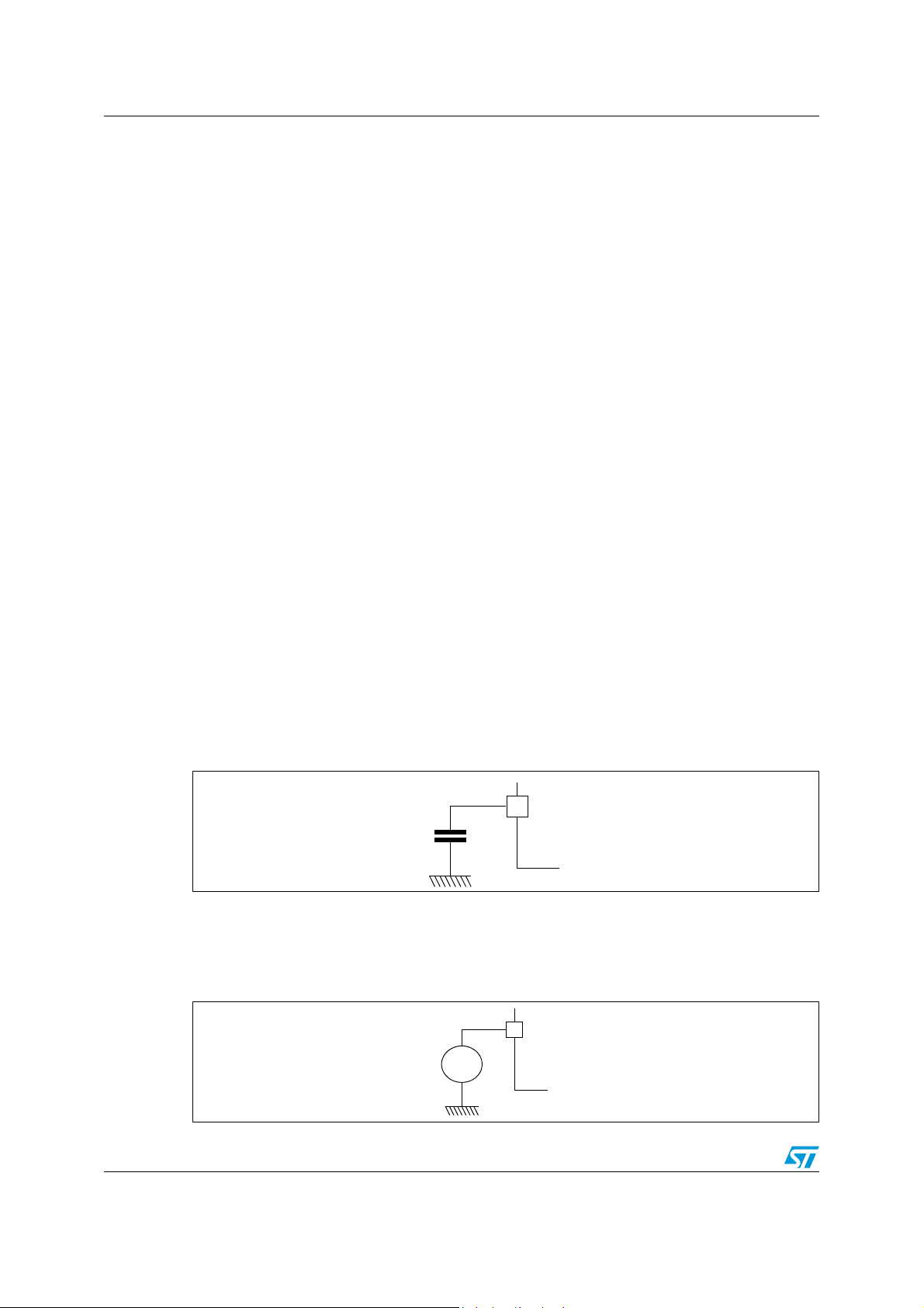
6.7 KOUTn/OPTn/GPOn pin characteristics
6.7.1 General characteristics
Subject to general operating conditions for VDD and TA unless otherwise specified.
Table 31. General characteristics
Symbol Parameter Conditions Min. Typ. Max. Unit
Input low level voltage
V
IL
Input high level voltage
V
IH
V
t
f(IO)out
t
r(IO)out
1. Not tested in production, guaranteed by characterization.
2. Data based on validation/design results.
Schmitt trigger voltage hysteresis
Hys
Input leakage current V
I
L
C
I/O pin capacitance 5 pF
IO
Output high to low level fall time
Output low to high level rise time
(1)
(1)
(2)
SS
CL = 50 pF
(2)
Between 10%
and 90%
(2)
≤ VIN ≤ V
VSS −0.3 0.3x V
0.7x V
DD
400 mV
DD
25
25
DD
VDD + 0.3
±1 μA
V
ns
6.7.2 Output pin characteristics
Subject to general operating conditions for VDD, f
Table 32. Output pin current
Symbol Parameter Conditions Min. Max. Unit
Output low level voltage for a high sink I/O
(1)
V
OL
V
OH
V
OL
V
OH
V
OL
V
OH
1. The IIO current sunk must always respect the absolute maximum rating specified in Table 22 and the sum
2. The IIO current sourced must always respect the absolute maximum rating specified in Table 22 and the
3. Not tested in production, based on characterization results.
pin when 4 pins are sunk at same time
(Figure 16)
Output high level voltage for an I/O pin
(2)
when 4 pins are sourced at same time
(Figure 21)
Output low level voltage for a high sink I/O
(1)(3)
pin when 4 pins are sunk at same time
Output high level voltage for an I/O pin
(2)(3)
when 4 pins are sourced at same time
(Figure 19)
Output low level voltage for a high sink I/O
(1)(3)
pin when 4 pins are sunk at same time
Output high level voltage for an I/O pin
(2)(3)
when 4 pins are sourced at same time
of IIO (I/O ports and control pins) must not exceed I
sum of I
(output and RESET pins) must not exceed I
IO
VSS
, and TA unless otherwise specified.
CPU
I
= +20mA 1.3
IO
I
= +8mA 0.75
IO
= 5V
I
= -5mA VDD−1.5
IO
DD
V
I
= -2mA VDD−0.8
IO
I
= +8mA 0.5
IO
= 3.3V
I
= -2mA VDD−0.8
DD
IO
V
I
= +8mA 0.6
IO
= 2.4V
I
= -2mA VDD−0.9
DD
IO
V
.
..
VDD
V
36/51
Page 37
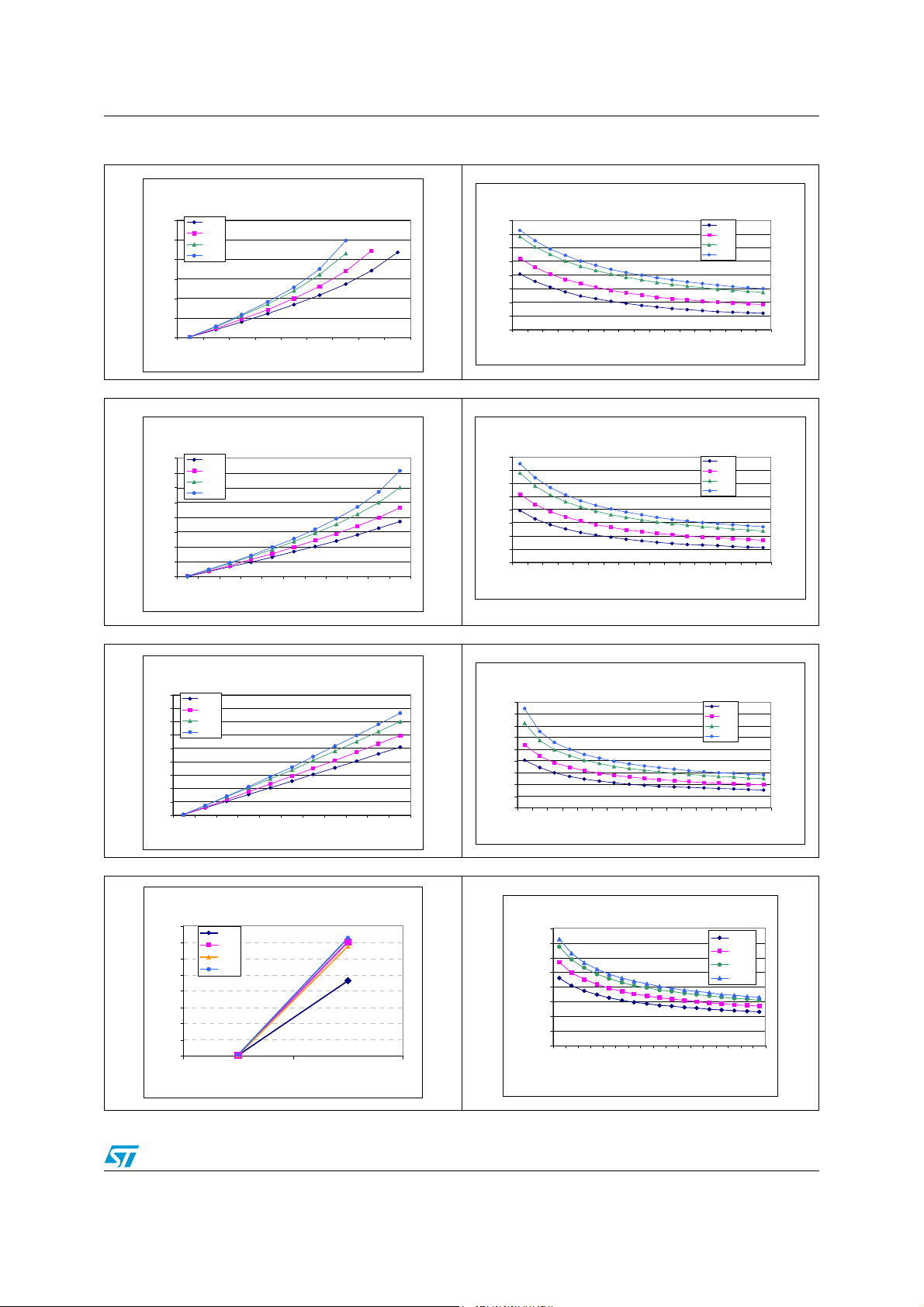
QST108 Electrical characteristics
VOL vs I
load
@ V
DD
= 2.4 V HS pins
0
200
400
600
800
1000
1200
0246810121416
I
load
[mA]
V
OL
[V]
-40°C
25°C
85°C
125°C
VOLvs VDD @I
load
=2 mA HS Pins
40
50
60
70
80
90
100
110
120
2.4 2.6 2.8 3 3.2 3.4 3.6 3.8 4 4.2 4.4 4.6 4.8 5 5.2 5.4 5.6
VDD [V]
V
OL
[mV]
-40°C
25°C
85°C
125°C
VOLvs I
load
@ V
DD
= 3 V HS pins
0
200
400
600
800
1000
1200
1400
1600
0 2 4 6 8 101214161820
I
load
[mA]
V
OL
[V]
-40°C
25°C
85°C
125°C
VOL vs VDD@I
load
= 8 mA HS Pins
140
190
240
290
340
390
440
490
540
2.4 2.6 2.8 3 3.2 3.4 3.6 3.8 4 4.2 4.4 4.6 4.8 5 5.2 5.4 5.6
VDD [V]
V
OL
[mV]
-40°C
25°C
85°C
125°C
VOL vs I
load
@ V
DD
= 5 V HS pins
0
100
200
300
400
500
600
700
800
900
02468101214161820
I
load
[mA]
V
OL
[V]
-40°C
25°C
85°C
125°C
VOL vs VDD @I
load
= 12 mA HS Pins
140
240
340
440
540
640
740
840
940
1040
2.4 2.6 2.8 3 3.2 3.4 3.6 3.8 4 4.2 4.4 4.6 4.8 5 5.2 5.4 5.6
VDD [V]
V
OL
[mV]
-40°C
25°C
85°C
125°C
VDD-VOH vs I
load
@ V
DD
= 2.4 V HS Pins
0
100
200
300
400
500
600
700
800
24
I
load
[mA]
V
DD
-V
OH
[mV]
-40°C
25°C
85°C
125°C
VDD-VOH vs VDD @I
load
= 2 mA HS Pin s
0
100
200
300
400
500
600
700
800
2.42.8
3.23.6
4
4.4
4.85.2
5.
6
VDD[V]
V
DD
-V
OH
[mV]
-40°C
25°C
85°C
125°C
Figure 11. Typical VOL at V
Figure 13. Typical VOL at V
= 2.4 V Figure 12. Typical VOL vs V
DD
= 3 V Figure 14. Typical VOL vs V
DD
DD
DD
at I
at I
load
load
= 2 mA
= 8 mA
Figure 15. Typical VOL at VDD = 5 V Figure 16. Typical VOL vs V
Figure 17. Typical VDD-VOH vs. I
load
at V
= 2.4 V Figure 18. Typical VDD-VOH vs. VDD at I
DD
DD
at I
= 12 mA
load
load
= 2 mA
37/51
Page 38

Electrical characteristics QST108
VDD-VOH vs I
load
@ V
DD
= 3 V HS Pins
0
200
400
600
800
1000
1200
1400
1600
1800
0246
I
load
[mA]
V
DD
-V
OH
[mV]
-40°C
25°C
85°C
125°C
VDD-VOH vs VDD @I
load
= 4 mA HS Pins
0
200
400
600
800
1000
1200
1400
1600
1800
2.
6
3
3.4
3.8
4.2
4.
6
5
5.
4
VDD [V]
V
DD
-V
OH
[mV]
-40°C
25°C
85°C
125°C
VDD-VOH vs I
load
@ V
DD
= 5 V HS Pin s
0
500
1000
1500
2000
2500
3000
3500
4000
4500
0 2 4 6 8 101214
I
load
[mA]
V
DD
-V
OH
[mV]
-40°C
25°C
85°C
125°C
Figure 19. Typical VDD-VOH vs. I
Figure 21. Typical VDD-VOH vs. I
load
load
at V
at V
= 3 V Figure 20. Typical VDD-VOH vs. V
DD
= 5 V
DD
DD
at I
load
= 4 mA
38/51
Page 39

QST108 Electrical characteristics
6.8 RESET pin
TA = -40°C to 125°C, unless otherwise specified.
Table 33. RESET pin characteristics
Symbol Parameter Conditions Min. Typ. Max. Unit
V
V
V
V
R
t
w(RSTL)out
t
h(RSTL)in
t
g(RSTL)in
1. Data based on characterization results, not tested in production.
2. The IIO current sunk must always respect the absolute maximum rating specified in Table 22: Current
characteristics on page 31 and the sum of IIO (I/O ports and control pins) must not exceed I
3. The RON pull-up equivalent resistor is based on a resistive transistor. Specified for voltages on RESET pin
between V
4. To guarantee the reset of the device, a minimum pulse has to be applied to the RESET pin. All short pulses
applied on RESET
IH
hys
OL
ON
Input low level voltage V
IL
Input high level voltage 0.7 x V
Schmitt trigger voltage
hysteresis
Output low level
voltage
Pull-up equivalent
resistor
Generated reset pulse
duration
External reset pulse
hold time
(2)
(3)
(4)
(1)
V
V
DD
IN
= V
= 5V I
SS
= +2mA 200 mV
IO
V
DD
V
DD
Internal reset sources 90
= 5V 30 50 70
= 3V 90
− 0.3 0.3x V
SS
DD
2V
(1)
(1)
20 μs
Filtered glitch duration 200 ns
and VDD.
ILmax
pin with a duration below t
h(RSTL)in
can be ignored.
V
VSS
DD
DD
+ 0.3
.
V
kΩ
μs
39/51
Page 40
Electrical characteristics QST108
2
C control interface
6.9
I
Subject to general operating conditions for VDD, and TA unless otherwise specified.
The QST108 I
2
C interface meets the requirements of the Standard I2C communication
protocol described in the following table with the restriction mentioned below:
Refer to I/O port characteristics for more details on the input/output alternate function
characteristics (SDA and SCL).
Table 34. I²C characteristics (100 kHz speed)
Symbol Parameter Min.
(1)
Max.
(1)
Unit
t
w(SCLL)
t
w(SCLH)
t
su(SDA)
t
h(SDA)
t
r(SDA)
t
r(SCL)
t
f(SDA)
t
f(SCL)
t
h(STA)
t
su(STA)
t
su(STO)
t
w(STO:STA)
C
Data based on standard I2C protocol requirement, not tested in production.
1.
2. The maximum hold time of the START condition has only to be met if the interface does not stretch the low
period of the SCL signal.
Table 35. IRQ specific pin characteristics
SCL clock low time 4.7
SCL clock high time 4.0
SDA setup time 250
SDA data hold time 0
(2)
SDA and SCL rise time 1000
SDA and SCL fall time 300
START condition hold time 4.0
Repeated START condition setup time 4.7
STOP condition setup time 4.0 μs
STOP to START condition time (bus free) 4.7 µs
Capacitive load for each bus line 400 pF
b
(1)
Symbol Parameter Conditions Min. Typ. Max. Unit
t
W(IRQ)
R
1. For additional pin parameters, please use the pin description in Section 6.7: KOUTn/OPTn/GPOn pin
2. The IRQ pull-up equivalent resistor is based on a resistive transistor.
IRQ pulse width 10 15 µs
V
= 5V 100 120 140
IRQ internal pull-up
IRQ
characteristics on page 36.
(2)
DD
= 3V 300
V
DD
µs
ns
ns
µs
kΩ
40/51
Page 41

QST108 Electrical characteristics
REPEATED START
START
STOP
START
t
f(SDA)
t
r(SDA)
t
su(SDA)th(SDA)
t
f(SCK)
t
r(SCK)
t
w(SCKL)
t
w(SCKH)
t
h(STA)
t
su(STO)
t
su(STA)tw(STO:STA)
SDA
SCL
4.7kΩ
SDA
QST device
SCL
V
DD
100Ω
100Ω
V
DD
4.7kΩ
I
2
CBUS
2
Figure 22.
Typical application with I
C bus and timing diagram
41/51
Page 42

Package mechanical data QST108
Seating
plane
C
AA2
A1
b
c
A1
L
L1
0.25 mm
Gage plane
K
D
D1
D3
24 17
16
25
E3 E1 E
932
18
Pin 1
identification
e
5V_ME
ccc
C
7 Package mechanical data
Figure 23. 32-pin low profile quad flat package (7x7) outline
42/51
Page 43

QST108 Package mechanical data
Table 36. 32-pin low profile quad flat package mechanical data
Dim.
mm inches
Min. Typ. Max. Min. Typ. Max.
A 1.600 0.0630
A1 0.050 0.150 0.0020 0.0059
A2 1.350 1.400 1.450 0.0531 0.0551 0.0571
b 0.300 0.370 0.450 0.0118 0.0146 0.0177
c 0.090 0.200 0.0035 0.0079
D 8.800 9.000 9.200 0.3465 0.3543 0.3622
D1 6.800 7.000 7.200 0.2677 0.2756 0.2835
D3 5.600 0.2205
E 8.800 9.000 9.200 0.3465 0.3543 0.3622
E1 6.800 7.000 7.200 0.2677 0.2756 0.2835
E3 5.600 0.2205
e 0.800 0.0315
L 0.450 0.600 0.750 0.0177 0.0236 0.0295
L1 1.000 0.0394
K 0.0° 3.5° 7.0° 0.0° 3.5° 7.0°
Tolerance (mm) Tolerance (inches)
ccc 0.10 0.0039
1. Values in inches are converted from mm and rounded to 4 decimal digits.
(1)
43/51
Page 44

Package mechanical data QST108
Ai15211
9
8
16
17
24
25
1
32
0.80
1.20
0.50
0.30
6.10
9.70
7.30
7.30
All dimensions are in millimeters.
6.10
9.70
1.20
Figure 24. 32-pin LQFP32 (7x7 mm) recommended footprint
44/51
Page 45

QST108 Package mechanical data
7.1 Soldering information
In accordance with the RoHS European directive, all STMicroelectronics packages have
been converted to lead-free technology, named ECOPACK™.
● ECOPACK™ packages are qualified according to the JEDEC STD-020C compliant
soldering profile.
● Detailed information on the STMicroelectronics ECOPACK™ transition program is
available on www.st.com/stonline/leadfree/, with specific technical Application notes
covering the main technical aspects related to lead-free conversion (AN2033, AN2034,
AN2035, and AN2036).
Backward and forward compatibility
The main difference between Pb and Pb-free soldering process is the temperature range.
● ECOPACK™ LQFP, SDIP, SO and DFN8 packages are fully compatible with Lead (Pb)
containing soldering process (see application note AN2034).
● LQFP, SDIP and SO Pb-packages are compatible with Lead-free soldering process,
nevertheless it's the customer's duty to verify that the Pb-packages maximum
temperature (mentioned on the Inner box label) is compatible with their Lead-free
soldering temperature.
Table 37. Soldering Compatibility (wave and reflow soldering process
Package Plating material devices Pb solder paste Pb-free solder paste
(1)
SDIP & PDIP Sn (pure Tin) Yes Yes
DFN8 Sn (pure Tin) Yes Yes
TQFP and SO NiPdAu (Nickel-palladium-Gold) Yes Yes
1. Assemblers must verify that the Pb-package maximum temperature (mentioned on the Inner box label) is
compatible with their Lead-free soldering process.
45/51
Page 46

Part numbering QST108
8 Part numbering
Table 38. Ordering information scheme
Example: QST 1 08 K T 6
Device type
QST = Capacitive touch sensor
Device sub-family
1: QTouch (3 to 5 V)
5: QMatrix (3 to 5 V)
6: QSlide/QWheel (3 to 5 V)
11: QTouch (1.8 to 3.6 V)
15: QMatrix (1.8 to 3.6 V)
16: QSlide/QWheel (1.8 to 3.6 V)
Channel count
Number of channels
Pin count
A: 8 pins S: 44 pins
Y: 16 pins C: 48 pins
K: 32 pins M: 80 pins
Package
B: DIP (dual in-line)
H: BGA (ball grid array)
M: SO (small outline)
N: TSSOP (thin-shrink small outline package)
T: LQFP (thin quad flat)
U: QFN (dual quad flat no lead)
Temperature range
0: +25°C 6: –40°C to +85°C
1: 0 to +70°C 7: –40°C to +105°C
5: –10°C to +85°C 9: –40°C to + 125°C
For a list of available options (speed, package, etc.) or for further information on any aspect
of this device, please contact your nearest ST Sales Office.
The category of second Level Interconnect is marked on the package and on the inner box
label, in compliance with JEDEC Standard JESD97. The maximum ratings related to
soldering conditions are also marked on the inner box label.
46/51
Page 47
QST108 Device revision information
QST108
QRG F01
A
B
C
DE
FG
H
IJ
K
a
9 Device revision information
9.1 Device revision identification
The marking on the right side of the second line (Line B) of the package top face identifies
the device revision.
Figure 25. Device revision identification (TQFP package)
Table 39. Device revision identification
Marking Device revision
F00 V 2.1
F01 V 2.3
The device revision can also be obtained using the GET_DEVICE_INFO I2C command. For
more information, refer to Section 4.9: Supported commands on page 16.
9.2 Device revision history
This section identifies the device deviations from the present specification for each device
revision.
9.2.1 Revision 2.1
Engineering samples. For more information regarding this revision, please contact your local
ST sales office.
47/51
Page 48

Device revision information QST108
9.2.2 Revision 2.3
● When the device enters Low Power mode, an additional sleep time is inserted after
each burst, instead of once after every complete burst cycle. As a result, if only one
burst is required, the sleep duration during Low Power mode is doubled. And if two
bursts are required, the sleep duration is tripled.
In Standalone mode, the 100ms sleep duration low power becomes either a 200ms or
300ms sleep duration depending on the number of bursts required.
In I2C mode, it is required to program a sleep duration for one half or a third of the
desired sleep duration depending on the number of bursts required.
● GET_PROTOCOL_VERSION returns 0x01 as I2CSpeed byte when it should return
0x00 (maximum speed is 100 kHz).
● If a command is sent with an incorrect parity bit, the device reports an unsupported
command instead of a parity error.
● In I2C mode, it is recommended to set the fast positive recalibration threshold to 5
using the SET_SCKEY_PARAMETERS command in order to ensure a reliable
behavior on low sensitivity keys.
● AKS should be always enabled in BCD mode. The AKS pull-up option resistor should
be connected to pin KOUT2.
48/51
Page 49

QST108 Revision history
10 Revision history
Table 40. Document revision history
Date Revision Changes
8-Jun-2007 1 Initial release.
15-Jun-2007 2 Datasheet status changed to Preliminary Data.
Removed Beeper function.
Changed LED output pins to GPO pins.
Updated pin names and functions in Section 2: Pin description on
page 5 and added Figure 2: QTouch™ measuring circuitry on
page 7.
Changed order of chapters in Section 3 for better comprehension.
Removed Simplified independent output mode from Section 4:
Device operating modes on page 11. Independent output mode
renamed Stand-alone mode.
Added Section 4.2: Reset and power-up on page 11 and removed
Power supply option chapter from Section 4.4.2: Option descriptions
26-Sep-2007 3
22-Nov-2007 4
on page 14.
Updated Table 6: Max On-Duration (MOD) truth table on page 14
and Table 7: Output mode (OM) truth table on page 15.
Updated Figure 3: Stand-alone mode typical schematic on page 13
and Figure 4: I2C mode typical schematic on page 16.
Updated Table 9: I²C address versus option resistor on page 18.
Added Figure 5: Optional LED schematic on page 17.
Updated Section 4.5: I2C mode on page 15.
Added Section 5.2.3: Key balance on page 25.
Updated Section 6.4: Supply current characteristics on page 31.
Added Section 6.5: Capacitive sensing characteristics on page 32.
and Section 6.7: RESET pin on page 36.
Updated Table 30: I²C characteristics on page 37.
Document status promoted from Preliminary Data to Datasheet.
Added ECOPACK® information.
Updated C
page 7.
Added Caution note in Section 3.10: Drift compensation on page 11.
Added Section 4.3: Low power mode on page 13.
Updated hex values in Table 9: I²C address versus option resistor on
page 21.
Updated Table 28: Supply current characteristics on page 34,
Table 30: Capacitive sensing parameters on page 35 and added
Figure 10: IDD Sleep mode current characteristics on page 34.
Added Table 35: IRQ specific pin characteristics on page 40.
Added Section 9: Device revision information on page 47.
value in Figure 2: QTouch™ measuring circuitry on
X
49/51
Page 50

Revision history QST108
Table 40. Document revision history (continued)
Date Revision Changes
Changed datasheet status to Not for new design.
Updated Figure 2: QTouch™ measuring circuitry to add RS sense
resistor.*
Updated Section 3.5: Detection integrator filter on page 9 and added
Figure 3: Detection signals on page 10.
Added Figure 4: Drift compensation example on page 12.
GET_KEY_ERROR and GET_KEY_STATE read values updated in
11-Jul-2008 5
Table 10: Supported commands on page 21 and updated note 3.
Updated bit values for Key activation description on page 25.
Added Section 6.3: EMC characteristics on page 32.
Updated Table 30: Capacitive sensing parameters on page 35.
Added Figure 24: 32-pin LQFP32 (7x7 mm) recommended footprint
on page 44.
Added Section 7.1: Soldering information on page 45.
Added Section 9.2.2: Revision 2.3 on page 48.
50/51
Page 51

QST108
Please Read Carefully:
Information in this document is provided solely in connection with ST products. STMicroelectronics NV and its subsidiaries (“ST”) reserve the
right to make changes, corrections, modifications or improvements, to this document, and the products and services described herein at any
time, without notice.
All ST products are sold pursuant to ST’s terms and conditions of sale.
Purchasers are solely responsible for the choice, selection and use of the ST products and services described herein, and ST assumes no
liability whatsoever relating to the choice, selection or use of the ST products and services described herein.
No license, express or implied, by estoppel or otherwise, to any intellectual property rights is granted under this document. If any part of this
document refers to any third party products or services it shall not be deemed a license grant by ST for the use of such third party products
or services, or any intellectual property contained therein or considered as a warranty covering the use in any manner whatsoever of such
third party products or services or any intellectual property contained therein.
UNLESS OTHERWISE SET FORTH IN ST’S TERMS AND CONDITIONS OF SALE ST DISCLAIMS ANY EXPRESS OR IMPLIED
WARRANTY WITH RESPECT TO THE USE AND/OR SALE OF ST PRODUCTS INCLUDING WITHOUT LIMITATION IMPLIED
WARRANTIES OF MERCHANTABILITY, FITNESS FOR A PARTICULAR PURPOSE (AND THEIR EQUIVALENTS UNDER THE LAWS
OF ANY JURISDICTION), OR INFRINGEMENT OF ANY PATENT, COPYRIGHT OR OTHER INTELLECTUAL PROPERTY RIGHT.
UNLESS EXPRESSLY APPROVED IN WRITING BY AN AUTHORIZED ST REPRESENTATIVE, ST PRODUCTS ARE NOT
RECOMMENDED, AUTHORIZED OR WARRANTED FOR USE IN MILITARY, AIR CRAFT, SPACE, LIFE SAVING, OR LIFE SUSTAINING
APPLICATIONS, NOR IN PRODUCTS OR SYSTEMS WHERE FAILURE OR MALFUNCTION MAY RESULT IN PERSONAL INJURY,
DEATH, OR SEVERE PROPERTY OR ENVIRONMENTAL DAMAGE. ST PRODUCTS WHICH ARE NOT SPECIFIED AS "AUTOMOTIVE
GRADE" MAY ONLY BE USED IN AUTOMOTIVE APPLICATIONS AT USER’S OWN RISK.
Resale of ST products with provisions different from the statements and/or technical features set forth in this document shall immediately void
any warranty granted by ST for the ST product or service described herein and shall not create or extend in any manner whatsoever, any
liability of ST.
ST and the ST logo are trademarks or registered trademarks of ST in various countries.
Information in this document supersedes and replaces all information previously supplied.
The ST logo is a registered trademark of STMicroelectronics. All other names are the property of their respective owners.
© 2008 STMicroelectronics - All rights reserved
STMicroelectronics group of companies
Australia - Belgium - Brazil - Canada - China - Czech Republic - Finland - France - Germany - Hong Kong - India - Israel - Italy - Japan -
Malaysia - Malta - Morocco - Singapore - Spain - Sweden - Switzerland - United Kingdom - United States of America
www.st.com
51/51
 Loading...