

1/89
PRELIMINARY DATA
February 2002
This is preliminary information on a new product now in development or undergoing evaluation. Details are subject to change without notice.
PSD834F2V
Flash PSD, 3.3V Supply, for 8-bit MCUs
2 Mbit + 256 Kbit Dual Flash Memories and 64 Kbit SRAM
FEATURES SUMMARY
■ Flash In-System Programmable (ISP)
Peripheral for 8-bit MCUs
■ 3.3 V±10% Single Supply Vo ltage
■ 2 Mbit of Primary Flash Memory (8 uniform
sectors, 32K x 8)
■ 256 Kbit Secondary Flash Memory (4 uniform
sectors)
■ 64 Kbit of battery-backed SRAM
■ Over 3,000 Gates of PLD: DPLD and CPLD
■ 27 Reconfigurable I/O ports
■ Enhanced JTAG Serial Port
■ Programmable power management
■ High Endurance:
– 100,000 Erase/Write Cycles of Flash Memory
– 1,000 Erase/Write Cycles of PLD
Figure 1. Packages
PLCC52 (K)
PQFP52 (T)

PSD834F2V
2/89
TABLE OF CONTENTS
Summary Description . . . . . . . . . . . . . . . . . . . . . . . . . . . . . . . . . . . . . . . . . . . . . . . . . . . . . . . . . . . . . . 5
Key Features . . . . . . . . . . . . . . . . . . . . . . . . . . . . . . . . . . . . . . . . . . . . . . . . . . . . . . . . . . . . . . . . . . . . . 6
PSD Architectural Overview . . . . . . . . . . . . . . . . . . . . . . . . . . . . . . . . . . . . . . . . . . . . . . . . . . . . . . . . . 8
Memory . . . . . . . . . . . . . . . . . . . . . . . . . . . . . . . . . . . . . . . . . . . . . . . . . . . . . . . . . . . . . . . . . . . . . . . 8
Page Register . . . . . . . . . . . . . . . . . . . . . . . . . . . . . . . . . . . . . . . . . . . . . . . . . . . . . . . . . . . . . . . . . . 8
PLDs . . . . . . . . . . . . . . . . . . . . . . . . . . . . . . . . . . . . . . . . . . . . . . . . . . . . . . . . . . . . . . . . . . . . . . . . . 8
I/O Ports . . . . . . . . . . . . . . . . . . . . . . . . . . . . . . . . . . . . . . . . . . . . . . . . . . . . . . . . . . . . . . . . . . . . . . 8
MCU Bus Interface . . . . . . . . . . . . . . . . . . . . . . . . . . . . . . . . . . . . . . . . . . . . . . . . . . . . . . . . . . . . . . 8
JTAG Port . . . . . . . . . . . . . . . . . . . . . . . . . . . . . . . . . . . . . . . . . . . . . . . . . . . . . . . . . . . . . . . . . . . . . 8
In-System Programming (ISP). . . . . . . . . . . . . . . . . . . . . . . . . . . . . . . . . . . . . . . . . . . . . . . . . . . . . . 9
Power Management Unit (PMU) . . . . . . . . . . . . . . . . . . . . . . . . . . . . . . . . . . . . . . . . . . . . . . . . . . . . 9
Development System. . . . . . . . . . . . . . . . . . . . . . . . . . . . . . . . . . . . . . . . . . . . . . . . . . . . . . . . . . . . . . 10
Pin Description. . . . . . . . . . . . . . . . . . . . . . . . . . . . . . . . . . . . . . . . . . . . . . . . . . . . . . . . . . . . . . . . . . . 11
PSD Register Description and Address Offset . . . . . . . . . . . . . . . . . . . . . . . . . . . . . . . . . . . . . . . . . 13
Detailed Operation. . . . . . . . . . . . . . . . . . . . . . . . . . . . . . . . . . . . . . . . . . . . . . . . . . . . . . . . . . . . . . . . 15
Memory Blocks . . . . . . . . . . . . . . . . . . . . . . . . . . . . . . . . . . . . . . . . . . . . . . . . . . . . . . . . . . . . . . . . . . 15
Primary Flash Memory and Secondary Flash m emo ry Description. . . . . . . . . . . . . . . . . . . . . . . . . 15
Memory Block Select Signals . . . . . . . . . . . . . . . . . . . . . . . . . . . . . . . . . . . . . . . . . . . . . . . . . . . . . 15
Instructions . . . . . . . . . . . . . . . . . . . . . . . . . . . . . . . . . . . . . . . . . . . . . . . . . . . . . . . . . . . . . . . . . . . . . 17
Power-down Instruction and Power-up Mode . . . . . . . . . . . . . . . . . . . . . . . . . . . . . . . . . . . . . . . . . 17
READ. . . . . . . . . . . . . . . . . . . . . . . . . . . . . . . . . . . . . . . . . . . . . . . . . . . . . . . . . . . . . . . . . . . . . . . . 17
Programming Flash Memory. . . . . . . . . . . . . . . . . . . . . . . . . . . . . . . . . . . . . . . . . . . . . . . . . . . . . . 19
Erasing Flash Memory. . . . . . . . . . . . . . . . . . . . . . . . . . . . . . . . . . . . . . . . . . . . . . . . . . . . . . . . . . . 20
Specific Features. . . . . . . . . . . . . . . . . . . . . . . . . . . . . . . . . . . . . . . . . . . . . . . . . . . . . . . . . . . . . . . 22
SRAM . . . . . . . . . . . . . . . . . . . . . . . . . . . . . . . . . . . . . . . . . . . . . . . . . . . . . . . . . . . . . . . . . . . . . . . 23
Sector Select and SRAM Select . . . . . . . . . . . . . . . . . . . . . . . . . . . . . . . . . . . . . . . . . . . . . . . . . . . 2 3
Page Register . . . . . . . . . . . . . . . . . . . . . . . . . . . . . . . . . . . . . . . . . . . . . . . . . . . . . . . . . . . . . . . . . 26

3/89
PSD834F2V
PLDs . . . . . . . . . . . . . . . . . . . . . . . . . . . . . . . . . . . . . . . . . . . . . . . . . . . . . . . . . . . . . . . . . . . . . . . . . . . 27
The Turbo Bit in PSD. . . . . . . . . . . . . . . . . . . . . . . . . . . . . . . . . . . . . . . . . . . . . . . . . . . . . . . . . . . . 27
Decode PLD (DPLD) . . . . . . . . . . . . . . . . . . . . . . . . . . . . . . . . . . . . . . . . . . . . . . . . . . . . . . . . . . . . 29
Complex PLD (CPLD) . . . . . . . . . . . . . . . . . . . . . . . . . . . . . . . . . . . . . . . . . . . . . . . . . . . . . . . . . . . 30
Output Macrocell (OMC) . . . . . . . . . . . . . . . . . . . . . . . . . . . . . . . . . . . . . . . . . . . . . . . . . . . . . . . . . 31
Product Term Allocator . . . . . . . . . . . . . . . . . . . . . . . . . . . . . . . . . . . . . . . . . . . . . . . . . . . . . . . . . . 3 2
Input Macrocells (IMC) . . . . . . . . . . . . . . . . . . . . . . . . . . . . . . . . . . . . . . . . . . . . . . . . . . . . . . . . . . 34
MCU Bus Interface. . . . . . . . . . . . . . . . . . . . . . . . . . . . . . . . . . . . . . . . . . . . . . . . . . . . . . . . . . . . . . . . 37
I/O Ports . . . . . . . . . . . . . . . . . . . . . . . . . . . . . . . . . . . . . . . . . . . . . . . . . . . . . . . . . . . . . . . . . . . . . . . . 45
General Port Architecture . . . . . . . . . . . . . . . . . . . . . . . . . . . . . . . . . . . . . . . . . . . . . . . . . . . . . . . . 45
Port Operating Modes . . . . . . . . . . . . . . . . . . . . . . . . . . . . . . . . . . . . . . . . . . . . . . . . . . . . . . . . . . . 47
MCU I/O Mode. . . . . . . . . . . . . . . . . . . . . . . . . . . . . . . . . . . . . . . . . . . . . . . . . . . . . . . . . . . . . . . . . 47
PLD I/O Mode . . . . . . . . . . . . . . . . . . . . . . . . . . . . . . . . . . . . . . . . . . . . . . . . . . . . . . . . . . . . . . . . . 47
Address Out Mode. . . . . . . . . . . . . . . . . . . . . . . . . . . . . . . . . . . . . . . . . . . . . . . . . . . . . . . . . . . . . . 47
Address In Mode . . . . . . . . . . . . . . . . . . . . . . . . . . . . . . . . . . . . . . . . . . . . . . . . . . . . . . . . . . . . . . . 48
Data Port Mode . . . . . . . . . . . . . . . . . . . . . . . . . . . . . . . . . . . . . . . . . . . . . . . . . . . . . . . . . . . . . . . . 48
Peripheral I/O Mode . . . . . . . . . . . . . . . . . . . . . . . . . . . . . . . . . . . . . . . . . . . . . . . . . . . . . . . . . . . . 48
JTAG In-System Programming (ISP) . . . . . . . . . . . . . . . . . . . . . . . . . . . . . . . . . . . . . . . . . . . . . . . 48
Port Configuration Registers (PCR) . . . . . . . . . . . . . . . . . . . . . . . . . . . . . . . . . . . . . . . . . . . . . . . . 48
Port Data Registers. . . . . . . . . . . . . . . . . . . . . . . . . . . . . . . . . . . . . . . . . . . . . . . . . . . . . . . . . . . . . 49
Ports A and B – Functionality and Structure . . . . . . . . . . . . . . . . . . . . . . . . . . . . . . . . . . . . . . . . . . 51
Port C – Functionality and Structure . . . . . . . . . . . . . . . . . . . . . . . . . . . . . . . . . . . . . . . . . . . . . . . . 52
Port D – Functionality and Structure . . . . . . . . . . . . . . . . . . . . . . . . . . . . . . . . . . . . . . . . . . . . . . . . 53
External Chip Select . . . . . . . . . . . . . . . . . . . . . . . . . . . . . . . . . . . . . . . . . . . . . . . . . . . . . . . . . . . . 53
Power Management . . . . . . . . . . . . . . . . . . . . . . . . . . . . . . . . . . . . . . . . . . . . . . . . . . . . . . . . . . . . . . . 55
PLD Power Management . . . . . . . . . . . . . . . . . . . . . . . . . . . . . . . . . . . . . . . . . . . . . . . . . . . . . . . . 58
PSD Chip Select Input (CSI, PD2) . . . . . . . . . . . . . . . . . . . . . . . . . . . . . . . . . . . . . . . . . . . . . . . . . 59
Input Clock. . . . . . . . . . . . . . . . . . . . . . . . . . . . . . . . . . . . . . . . . . . . . . . . . . . . . . . . . . . . . . . . . . . . 59
Input Control Signals. . . . . . . . . . . . . . . . . . . . . . . . . . . . . . . . . . . . . . . . . . . . . . . . . . . . . . . . . . . . 59

PSD834F2V
4/89
Reset Timing and Device Status at Reset . . . . . . . . . . . . . . . . . . . . . . . . . . . . . . . . . . . . . . . . . . . . .60
Warm Reset. . . . . . . . . . . . . . . . . . . . . . . . . . . . . . . . . . . . . . . . . . . . . . . . . . . . . . . . . . . . . . . . . . . 6 0
I/O Pin, Register and PLD Status at Reset . . . . . . . . . . . . . . . . . . . . . . . . . . . . . . . . . . . . . . . . . . . 60
Reset of Flash Memory Erase and Program Cycles . . . . . . . . . . . . . . . . . . . . . . . . . . . . . . . . . . . . 60
Programming In-Circuit using the JTAG Serial Interface . . . . . . . . . . . . . . . . . . . . . . . . . . . . . . . . 61
Standard JTAG Signals. . . . . . . . . . . . . . . . . . . . . . . . . . . . . . . . . . . . . . . . . . . . . . . . . . . . . . . . . . 61
JTAG Extensions . . . . . . . . . . . . . . . . . . . . . . . . . . . . . . . . . . . . . . . . . . . . . . . . . . . . . . . . . . . . . . . 61
Security and Flash memory Protection . . . . . . . . . . . . . . . . . . . . . . . . . . . . . . . . . . . . . . . . . . . . . .62
AC/DC Parameters. . . . . . . . . . . . . . . . . . . . . . . . . . . . . . . . . . . . . . . . . . . . . . . . . . . . . . . . . . . . . . . . 63
Table: Absolute Maximum Ratings . . . . . . . . . . . . . . . . . . . . . . . . . . . . . . . . . . . . . . . . . . . . . . . . .66
Table: Operating Conditions . . . . . . . . . . . . . . . . . . . . . . . . . . . . . . . . . . . . . . . . . . . . . . . . . . . . . . 67
Table: DC Characteristics . . . . . . . . . . . . . . . . . . . . . . . . . . . . . . . . . . . . . . . . . . . . . . . . . . . . . . . . 69
Table: CPLD Combinatorial Timing. . . . . . . . . . . . . . . . . . . . . . . . . . . . . . . . . . . . . . . . . . . . . . . . .70
Table: CPLD Macrocell Synchronous Clock Mode Timing . . . . . . . . . . . . . . . . . . . . . . . . . . . . . . . 70
Table: CPLD Macrocell Asynchronous Clock Mode Timing . . . . . . . . . . . . . . . . . . . . . . . . . . . . . . 71
Table: Input Macrocell Timing . . . . . . . . . . . . . . . . . . . . . . . . . . . . . . . . . . . . . . . . . . . . . . . . . . . . . 73
Table: Read Timing . . . . . . . . . . . . . . . . . . . . . . . . . . . . . . . . . . . . . . . . . . . . . . . . . . . . . . . . . . . . . 74
Table: Write Timing . . . . . . . . . . . . . . . . . . . . . . . . . . . . . . . . . . . . . . . . . . . . . . . . . . . . . . . . . . . . . 76
Table: Program, Write and Erase Times. . . . . . . . . . . . . . . . . . . . . . . . . . . . . . . . . . . . . . . . . . . . . 77
Table: Port A Peripheral Data Mode Read Timing . . . . . . . . . . . . . . . . . . . . . . . . . . . . . . . . . . . . . 78
Table: Port A Peripheral Data Mode Write Timing . . . . . . . . . . . . . . . . . . . . . . . . . . . . . . . . . . . . . 78
Table: Reset (Reset) Timing . . . . . . . . . . . . . . . . . . . . . . . . . . . . . . . . . . . . . . . . . . . . . . . . . . . . . . 80
Table: VSTBYON Timing . . . . . . . . . . . . . . . . . . . . . . . . . . . . . . . . . . . . . . . . . . . . . . . . . . . . . . . . . 80
Table: ISC Timing . . . . . . . . . . . . . . . . . . . . . . . . . . . . . . . . . . . . . . . . . . . . . . . . . . . . . . . . . . . . . .80
Table: Power-down Timing . . . . . . . . . . . . . . . . . . . . . . . . . . . . . . . . . . . . . . . . . . . . . . . . . . . . . . . 81
Package Mechanical . . . . . . . . . . . . . . . . . . . . . . . . . . . . . . . . . . . . . . . . . . . . . . . . . . . . . . . . . . . . . . 82
Table: PLCC52 – 52 lead Plastic Leaded Chip Carrier, rectangular. . . . . . . . . . . . . . . . . . . . . . . . 83
Table: Pin Assignments – PLCC52 . . . . . . . . . . . . . . . . . . . . . . . . . . . . . . . . . . . . . . . . . . . . . . . . .84
Table: PQFP52 - 52 lead Plastic Quad Flatpack. . . . . . . . . . . . . . . . . . . . . . . . . . . . . . . . . . . . . . . 85
Table: Pin Assignments – PQFP52. . . . . . . . . . . . . . . . . . . . . . . . . . . . . . . . . . . . . . . . . . . . . . . . .86
Table: Ordering Information Scheme . . . . . . . . . . . . . . . . . . . . . . . . . . . . . . . . . . . . . . . . . . . . . . .87

5/89
PSD834F2V
SUMMARY DESCRIPTION
The PSD family of memory systems for microcontrollers (MCUs) brings In-System-Programmability
(ISP) to Flash memory and programmable logic.
The result is a simple and flexible solution for embedded designs. PSD dev ices combine many of
the peripheral functions found in MCU based applications.
The CPLD in the PSD devices features an optimized macrocell logic architecture. The PSD macrocell was created to address the unique
requirements of embedded system designs. It allows direct connection between the system address/data bus, and the internal PSD registers, to
simplify communication between the MCU and
other supporting devices.
The PSD device includes a JTAG Serial Programming interface, to allow In-System Programming
(ISP) of the
entire device
. This feature reduces development time, simplifies the manufacturing flow,
and dramatically lowers the cost of field upgrades.
Using ST’s special Fast-JTAG programming, a design can be rapidly programmed into the PSD in as
little as seven seconds.
The innovative PSD family solves key problems
faced by designers when managing discrete Flash
memory devices, such as:
– First-time In-System Programming (ISP)
– Complex address decoding
– Simulataneou s read and write to the device.
The JTAG Serial Interface block allows In-System
Programming (ISP), and e liminates the need for
an external Boot EPROM, or an external programmer. To simplify Flash memory updates, program
execution is performed from a secondary Flash
memory while the primary Flash memory is being
updated. This solution avoids the complicated
hardware and software overhead necessary to implement IAP.
ST makes available a software devel opment tool,
PSDsoft Express, that generates ANSI -C compliant code for use with your target M CU. T his c ode
allows you to manipulate the non-v olatile me mory
(NVM) within the PSD. Code exam ples are also
provided for:
– Flash memory IAP via the UART of the host
MCU
– Memory paging to execute code across several
PSD memory pages
– Loading, reading, and manipulation of PSD
macrocells by the MCU.

PSD834F2V
6/89
KEY FEATURES
■ A simple interface to 8-bit microcontrollers that
use either multiplexed or non-multiplexed
busses. The bus interface logic uses the control
signals generated by the microcontroller
automatically when the address is decoded and
a read or write is performed. A partial list of the
MCU families supported include:
– Intel 8031, 80196, 80186, 80C251, and
80386EX
– Motorola 68HC11, 68HC16, 68HC12, and
683XX
– Philips 8031 and 8051XA
– Zilog Z80 and Z8
■ Internal 2 Mbit Flash memory. This is the main
Flash memory. It is divided into 8 equal-sized
blocks that can b e accessed with user-specifi ed
addresses.
■ Internal secondary 256 Kbit Flash boot memory.
It is divided into 4 equal-sized blocks that can be
accessed with user-specified addresses. This
secondary memory brings the ability to execute
code and update the main Flash
concurrently
.
■ Intern al 64 Kbit SRAM. The SRAM’s conte n ts
can be protected from a power failure by
connecting an external battery.
■ CPLD with 16 Output macrocells (OMCs) and
24 Input macrocells (IMCs). The CPLD may be
used to efficiently implement a variety of logic
functions for internal and external control.
Examples include state machines, loadable
shift registers, and loadable counters.
■ Decode PLD (DPLD) that decodes address for
selection of internal memory blocks.
■ 27 individually configurable I/O port pins that
can be used for the following functions:
– MCU I/Os
–PLD I/Os
– Latched MCU address output
– Special function I/Os.
– 16 of the I/O ports may be configured as
open-drain outputs.
■ Standby current as low as 25 µA.
■ Built-in JTAG compliant serial port allows full-
chip In-System Programmability (ISP). With it,
you can program a blank device or reprogram a
device in the factory or the field.
■ Internal page register that can be used to
expand the microcontroller address space by a
factor of 256.
■ Internal programmable Power Management
Unit (PMU) that supports a low power mode
called Power Down Mode. The PMU can
automatically detect a lack of microcontroller
activity and put the PSD into Power-down
mode.
■ Erase/Write cycles:
– Flash memory – 100,000 minimum
– PLD – 1,000 minimum
– Data Retention: 15 year minimum (for Main
Flash memory, Boot , PLD a nd Configurat ion
bits)
7/89
PSD834F2V
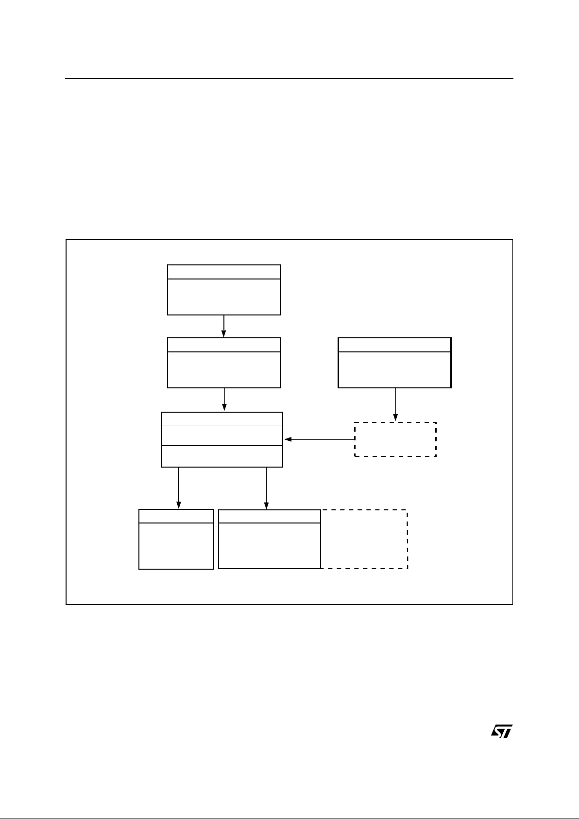
Figure 2. PSD B l ock Di a gra m
PROG.
MCU BUS
INTRF.
ADIO
PORT
CNTL0,
CNTL1,
CNTL2
AD0 – AD15
CLKIN
(PD1)
CLKIN
CLKIN
PLD
INPUT
BUS
PROG.
PORT
PORT
A
PROG.
PORT
PORT
B
POWER
MANGMT
UNIT
2 MBIT PRIMARY
FLASH MEMORY
8 SECTORS
VSTDBY
PA0 – PA7
PB0 – PB7
PROG.
PORT
PORT
C
PROG.
PORT
PORT
D
PC0 – PC7
PD0 – PD2
ADDRESS/DATA/CONTROL BUS
PORT A ,B & C
3 EXT CS TO PORT D
24 INPUT MACROCELLS
PORT A ,B & C
73
73
256 KBIT SECONDARY
NON-VOLATILE MEMORY
(BOOT OR DATA)
4 SECTORS
64 KBIT BATTERY
BACKUP SRAM
RUNTIME CONTROL
AND I/O REGISTERS
SRAM SELECT
PERIP I/O MODE SELECTS
MACROCELL FEEDBACK OR PORT INPUT
CSIOP
FLASH ISP CPLD
(CPLD)
16 OUTPUT MACROCELLS
FLASH DECODE
PLD
(
DPLD
)
PLD, CONFIGURATION
& FLASH MEMORY
LOADER
JTAG
SERIAL
CHANNEL
(
PC2
)
PAGE
REGISTER
EMBEDDED
ALGORITHM
SECTOR
SELECTS
SECTOR
SELECTS
GLOBAL
CONFIG. &
SECURITY
AI05793
8
PSD834F2V
8/89
PSD ARCHITECTURAL OVERVIEW
PSD devices contain several major functional
blocks. Figur e 2 shows the architect ure of the PSD
device family. The functions of each block are described briefly in the following sections. Many of
the blocks perform multiple functions and are user
configurable.
Memory
Each of the memory blocks is briefly discussed in
the following paragraphs. A more detailed discus-
sion can be found in the section entitled “Memory
Blocks“ on page 15.
The 2 Mbit (256K x 8) Flash m emory is the primary
memory of the PSD. It is divided into 8 equallysized sectors that are individually selectable.
The 256 Kbit (32K x 8) se condary Flash memory
is divided into 4 equally-sized sectors. Each sector
is individually selectable.
The 64 Kbit SRAM is intended for use as a
scratch-pad memory or as an extension to the
MCU SRAM. If an external battery is connected to
Voltage Stand-by (VSTBY, PC2), data is retained
in the event of power failure.
Each sector of mem ory c an be l oc ated in a dif ferent address space as defined by the user. The access times for all memory types includes the
address latching and DPLD decoding time.
Page Re gi st er
The 8-bit Page Register expands the address
range of the MCU by up to 256 times. The paged
address can be used as part of the address space
to access external memory and peripherals, or internal memory and I/O. The Page Register can
also be used to change the address mapping of
sectors of the Flash memories into different memory spaces for IAP.
PLDs
The device contains tw o PLDs, the Decode PLD
(DPLD) and the Complex PLD (CPLD), as shown
in Table 1, each op timized for a di fferent fun ction.
The functional partitioning of the PLDs reduces
power consumption, optimizes cost/performance,
and eases design entry.
Table 1. PLD I/O
The DPLD is used to decode addresses and to
generate Sector Select signals for the PSD internal memory and regis ters. The DPLD has combinatorial outputs. The CPLD has 16 Output
Macrocells (OMC) and 3 combinatorial outputs.
The PSD also has 24 Input Macrocells (IMC) that
can be configured as inputs to the PLDs. The
PLDs receive their inputs from the PLD Input Bus
and are differentiated by their output destinations,
number of product terms, and macrocells.
The PLDs consume minimal power. The speed
and power consumption of the PLD i s controlled
by the Turbo bit in PMMR0 and other bits in the
PMMR2. These registers are set by the MCU at
run-time. There is a slight penalty to PLD propagation time when invoking the power m anagement
features.
I/O Po r t s
The PSD has 27 individually configurable I/O pins
distributed over the four ports (Port A, B, C, and
D). Each I/O pin can be individually configured for
different functions. Ports can be configured as
standard MCU I/O ports, PLD I/O, or latched address outputs for MCUs using multiplexed address/data buses.
The JTAG pins can be enabled on Po rt C for InSystem Programming (ISP).
Ports A and B can also be conf igured as a data
port for a non-multiplexed bus.
MCU Bus Interface
PSD interfaces easily with most 8-bit MCUs that
have either multiplexed or non-multiplexed address/data buses. The device is configured to respond to the MCU’s control signals, which are also
used as inputs to the PLDs. For examples, please
see the section entitled “MCU Bus Interface Examples“ on page 39.
Table 2. JTAG SIgnals on Port C
JTAG Port
In-System Programming (ISP) can be pe rformed
through the JTAG signals on Port C. This serial interface allows complete programming of the entire
PSD device. A blank device can be completely
programmed. The JTAG signals (TMS, TCK,
TSTAT
, TERR, TDI, TDO) can be multiplexed with
other functions on Port C. Table 2 indicates the
JTAG pin assignments.
Name Inputs Outputs
Product
Terms
Decode PLD (DPLD) 73 17 42
Complex PLD (CPLD) 73 19 140
Port C Pins JTAG Signal
PC0 TMS
PC1 TCK
PC3 TSTAT
PC4 TERR
PC5 TDI
PC6 TDO
9/89
PSD834F2V
In-System Progr a mming (ISP)
Using the JTAG signals on Port C, the entire PSD
device can be programmed or erased wit hout the
use of the MCU. The primary Flash memory can
also be programmed in-system by the M CU executing the programming algorithms out of the secondary memory, or SRAM. The secondary
memory can be programmed the same way by executing out of the primary Flash memory. The PLD
or other PSD Configuration blocks can be programmed through the J TAG port or a de vice programmer. Table 3 indicates which programming
methods can program different functional blo cks
of the PSD.
Table 3. Methods of Programming Different Functional Blocks of the PSD
Power Management Unit (PMU)
The Power Management Unit (PMU) gives the
user control of the power consumption on selected
functional blocks based on system req uirements.
The PMU includes an Automatic Power-down
(APD) Unit that turns off device functions during
MCU inactivity. The APD Unit has a Power-down
mode that helps reduce power consumption.
The PSD also has some bits that are configured at
run-time by the MCU to reduce power consumption of the CPLD. The Turbo bit in PMMR0 can be
reset to 0 and the CPLD l atches its outputs and
goes to sleep until the next transition on its inputs.
Additionally, bits in PMMR2 can be set by the
MCU to block signals from entering the CPLD t o
reduce power consumption. Please s ee the sec-
tion entitled “Power Management” on page 55 for
more details.
Functional Block JTAG Programming Device Programmer IAP
Primary Flash Memory Yes Yes Yes
Secondary Flash Memory Yes Yes Yes
PLD Array (DPLD and CPLD) Yes Yes No
PSD Configuration Yes Yes No
PSD834F2V
10/89
DEVELOPMENT SYST EM
The PSD family is supported by PSDsoft Express,
a Windows-based software development tool. A
PSD design is quicly and easily produced in a
point and click environment. The designer does
not need to enter Hardware Description Language
(HDL) equations, unless desired, to define PSD
pin functions and memo ry map information. The
general design flow is shown in Figure 3. PSDsoft
Express is available from our web site (the ad-
dress is given on the back page of this data sheet)
or other distribution channels.
PSDsoft Express directly supports two low cost
device programmers form ST: PSDpro and
FlashLINK (JTAG). Both of these programmers
may be purchased through your local distributor/
representative, or directly from our web site using
a credit card. The PSD is also supported by t hid
party device programmers. See our web site for
the current list.
Figure 3. PSDsoft Express Developmen t Tool
PSD Configuration
PSD Fitter
PSD Simulator
PSD Programmer
*.OBJ FILE
PLD DESCRIPTION
CONFIGURE MCU BUS
INTERFACE AND OTHER
PSD ATTRIBUTES
LOGIC SYNTHESIS
AND FITTING
PSDsilos III
DEVICE SIMULATION
(OPTIONAL)
PSDPro, or
FlashLINK (JTAG)
ADDRESS TRANSLATION
AND MEMORY MAPPING
PSDabel
MODIFY ABEL TEMPLATE FILE
OR GENERATE NEW FILE
PSD TOOLS
GENERATE C CODE
SPECIFIC TO PSD
FUNCTIONS
USER'S CHOICE OF
MICROCONTROLLER
COMPILER/LINKER
*.OBJ AND *.SVF
FILES AVAILABLE
FOR 3rd PARTY
PROGRAMMERS
(CONVENTIONAL or
JTAG-ISC)
FIRMWARE
HEX OR S-RECORD
FORMAT
AI04918
11/89
PSD834F2V
PIN DESCRIPTION
Table 4 describes the signal names and signal
functions of the PSD.
Table 4. Pin Description (for the PLCC52 package
1
)
Pin Name Pin Type Description
ADIO0-7 30-37 I/O
This is the lower Address/Data port. Connect your MCU address or address/data bus
according to the following rules:
1. If your MCU has a multiplexed address/data bus where the data is multiplexed with the
lower address bits, connect AD0-AD7 to this port.
2. If your MCU does not have a multiplexed address/data bus, or you are using an
80C251 in page mode, connect A0-A7 to this port.
3. If you are using an 80C51XA in burst mode, connect A4/D0 through A11/D7 to this
port.
ALE or AS latches the address. The PSD drives data out only if the read signal is active
and one of the PSD functional blocks was selected. The addresses on this port are
passed to the PLDs.
ADIO8-15 39-46 I/O
This is the upper Address/Data port. Connect your MCU address or address/data bus
according to the following rules:
1. If your MCU has a multiplexed address/data bus where the data is multiplexed with the
lower address bits, connect A8-A15 to this port.
2. If your MCU does not have a multiplexed address/data bus, connect A8-A15 to this
port.
3. If you are using an 80C251 in page mode, connect AD8-AD15 to this port.
4. If you are using an 80C51XA in burst mode, connect A12/D8 through A19/D15 to this
port.
ALE or AS latches the address. The PSD drives data out only if the read signal is active
and one of the PSD functional blocks was selected. The addresses on this port are
passed to the PLDs.
CNTL0 47 I
The following control signals can be connected to this port, based on your MCU:
1. WR
– active Low Write Strobe input.
2. R_W
– active High read/active Low write input.
This port is connected to the PLDs. Therefore, these signals can be used in decode and
other logic equations.
CNTL1 50 I
The following control signals can be connected to this port, based on your MCU:
1. RD
– active Low Read Strobe input.
2. E – E clock input.
3. DS
– active Low Data Strobe input.
4. PSEN
– connect PSEN to this port when it is being used as an active Low read signal.
For example, when the 80C251 outputs more than 16 address bits, PSEN
is actually the
read signal.
This port is connected to the PLDs. Therefore, these signals can be used in decode and
other logic equations.
CNTL2 49 I
This port can be used to input the PSEN
(Program Select Enable) signal from any MCU
that uses this signal for code exclusively. If your MCU does not output a Program Select
Enable signal, this port can be used as a generic input. This port is connected to the
PLDs.
Reset
48 I
Resets I/O Ports, PLD macrocells and some of the Configuration Registers. Must be Low
at Power-up.
PSD834F2V
12/89
PA0
PA1
PA2
PA3
PA4
PA5
PA6
PA7
29
28
27
25
24
23
22
21
I/O
These pins make up Port A. These port pins are configurable and can have the following
functions:
1. MCU I/O – write to or read from a standard output or input port.
2. CPLD macrocell (McellAB0-7) outputs.
3. Inputs to the PLDs.
4. Latched address outputs (see Table 5).
5. Address inputs. For example, PA0-3 could be used for A0-A3 when using an 80C51XA
in burst mode.
6. As the data bus inputs D0-D7 for non-multiplexed address/data bus MCUs.
7. D0/A16-D3/A19 in M37702M2 mode.
8. Peripheral I/O mode.
Note: PA0-PA3 can only output CMOS signals with an option for high slew rate. However,
PA4-PA7 can be configured as CMOS or Open Drain Outputs.
PB0
PB1
PB2
PB3
PB4
PB5
PB6
PB7
7
6
5
4
3
2
52
51
I/O
These pins make up Port B. These port pins are configurable and can have the following
functions:
1. MCU I/O – write to or read from a standard output or input port.
2. CPLD macrocell (McellAB0-7 or McellBC0-7) outputs.
3. Inputs to the PLDs.
4. Latched address outputs (see Table 5).
Note: PB0-PB3 can only output CMOS signals with an option for high slew rate. However,
PB4-PB7 can be configured as CMOS or Open Drain Outputs.
PC0 20 I/O
PC0 pin of Port C. This port pin can be configured to have the following functions:
1. MCU I/O – write to or read from a standard output or input port.
2. CPLD macrocell (McellBC0) output.
3. Input to the PLDs.
4. TMS Input
2
for the JTAG Serial Interface.
This pin can be configured as a CMOS or Open Drain output.
PC1 19 I/O
PC1 pin of Port C. This port pin can be configured to have the following functions:
1. MCU I/O – write to or read from a standard output or input port.
2. CPLD macrocell (McellBC1) output.
3. Input to the PLDs.
4. TCK Input
2
for the JTAG Serial Interface.
This pin can be configured as a CMOS or Open Drain output.
PC2 18 I/O
PC2 pin of Port C. This port pin can be configured to have the following functions:
1. MCU I/O – write to or read from a standard output or input port.
2. CPLD macrocell (McellBC2) output.
3. Input to the PLDs.
4. VSTBY – SRAM stand-by voltage input for SRAM battery backup.
This pin can be configured as a CMOS or Open Drain output.
PC3 17 I/O
PC3 pin of Port C. This port pin can be configured to have the following functions:
1. MCU I/O – write to or read from a standard output or input port.
2. CPLD macrocell (McellBC3) output.
3. Input to the PLDs.
4. TSTAT
output2 for the JTAG Serial Interface.
5. Ready/Busy
output for parallel In-System Programming (ISP).
This pin can be configured as a CMOS or Open Drain output.
PC4 14 I/O
PC4 pin of Port C. This port pin can be configured to have the following functions:
1. MCU I/O – write to or read from a standard output or input port.
2. CPLD macrocell (McellBC4) output.
3. Input to the PLDs.
4. TERR
output2 for the JTAG Serial Interface.
5. Battery-on Indicator (VBATON). Goes High when power is being drawn from the
external battery.
This pin can be configured as a CMOS or Open Drain output.
Pin Name Pin Type Description
13/89
PSD834F2V
Note: 1. The pi n numbers in th i s t abl e are for the PLCC package only. See the package inf ormation, on page 83 onwards, for pin nu mb ers
on other package types.
2. These func tions can be multiplexe d wi th other functions.
PSD REGISTER DESCRIPTION AND ADDRESS OFFSET
Table 6 shows the offset addresses to the PSD
registers relative to the CSIOP base address. The
CSIOP space is the 256 bytes of address that is allocated by the user to the internal PS D registers.
Table 6 provides brief descriptions of the registers
in CSIOP space. The following section gives a
more detailed description.
PC5 13 I/O
PC5 pin of Port C. This port pin can be configured to have the following functions:
1. MCU I/O – write to or read from a standard output or input port.
2. CPLD macrocell (McellBC5) output.
3. Input to the PLDs.
4. TDI input
2
for the JTAG Serial Interface.
This pin can be configured as a CMOS or Open Drain output.
PC6 12 I/O
PC6 pin of Port C. This port pin can be configured to have the following functions:
1. MCU I/O – write to or read from a standard output or input port.
2. CPLD macrocell (McellBC6) output.
3. Input to the PLDs.
4. TDO output
2
for the JTAG Serial Interface.
This pin can be configured as a CMOS or Open Drain output.
PC7 11 I/O
PC7 pin of Port C. This port pin can be configured to have the following functions:
1. MCU I/O – write to or read from a standard output or input port.
2. CPLD macrocell (McellBC7) output.
3. Input to the PLDs.
4. DBE – active Low Data Byte Enable input from 68HC912 type MCUs.
This pin can be configured as a CMOS or Open Drain output.
PD0 10 I/O
PD0 pin of Port D. This port pin can be configured to have the following functions:
1. ALE/AS input latches address output from the MCU.
2. MCU I/O – write or read from a standard output or input port.
3. Input to the PLDs.
4. CPLD output (External Chip Select).
PD1 9 I/O
PD1 pin of Port D. This port pin can be configured to have the following functions:
1. MCU I/O – write to or read from a standard output or input port.
2. Input to the PLDs.
3. CPLD output (External Chip Select).
4. CLKIN – clock input to the CPLD macrocells, the APD Unit’s Power-down counter, and
the CPLD AND Array.
PD2 8 I/O
PD2 pin of Port D. This port pin can be configured to have the following functions:
1. MCU I/O – write to or read from a standard output or input port.
2. Input to the PLDs.
3. CPLD output (External Chip Select).
4. PSD Chip Select Input (CSI
). When Low, the MCU can access the PSD memory and I/
O. When High, the PSD memory blocks are disabled to conserve power.
V
CC
15, 38 Supply Voltage
GND
1, 16,
26
Ground pins
Pin Name Pin Type Description
PSD834F2V
14/89
Table 5. I/O Port Latched Address Output Assignments
1
Note: 1. See the section entitled “I /O Ports”, on page 45, on how to enable the Lat ched Addre ss Output fun ct i on.
2. N/A = Not Applicable
Table 6. Register Address Offset
Note: 1. Other registers that are not part of the I/O ports.
MCU
Port A Port B
Port A (3:0) Port A (7:4) Port B (3:0) Port B (7:4)
8051XA (8-bit) N/A Address a7-a4 Address a11-a8 N/A
80C251 (page mode) N/A N/A Address a11-a8 Address a15-a12
All other 8-bit multiplexed Address a3-a0 Address a 7-a4 Address a 3-a0 Address a7-a4
8-bit non-multiplexed bus N/A N/A Address a3-a0 Address a7-a4
Register Name Port A Port B Port C Port D
Other
1
Description
Data In 00 01 10 11 Reads Port pin as input, MCU I/O input mode
Control 02 03 Selects mode between MCU I/O or Address Out
Data Out 04 05 12 13
Stores data for output to Port pins, MCU I/O output
mode
Direction 06 07 14 15 Configures Port pin as input or output
Drive Select 08 09 16 17
Configures Port pins as either CMOS or Open
Drain on some pins, while selecting high slew rate
on other pins.
Input Macrocell 0A 0B 18 Reads Input Macrocells
Enable Out 0C 0D 1A 1B
Reads the status of the output enable to the I/O
Port driver
Output Macrocells
AB
20 20
Read – reads output of macrocells AB
Write – loads macrocell flip-flops
Output Macrocells
BC
21 21
Read – reads output of macrocells BC
Write – loads macrocell flip-flops
Mask Macrocells AB 22 22 Blocks writing to the Output Macrocells AB
Mask Macrocells BC 23 23 Blocks writing to the Output Macrocells BC
Primary Flash
Protection
C0 Read only – Primary Flash Sector Protection
Secondary Flash
memory Protection
C2
Read only – PSD Security and Secondary Flash
memory Secto r Protection
JTAG Enable C7 Enables JTAG Port
PMMR0 B0 Power Management Register 0
PMMR2 B4 Power Management Register 2
Page E0 Page Register
VM E2
Places PSD memory areas in Program and/or
Data space on an individual basis.

15/89
PSD834F2V
DETAILED OPERATION
As shown in Figure 2, the PSD consists of six major types of functional blocks:
■ Memory Blo c k s
■ PLD Bl o c ks
■ MCU Bus Interface
■ I/O Por ts
■ Power Management Unit (PMU)
■ JTAG In te rfac e
The functions of ea ch block are described i n the
following sections. Many of the blocks perform
multiple functions, and are user configurable.
MEMORY BLOCKS
The PSD has the following memory blocks:
– Primary Flash memory
– Secondary Flash memory
–SRAM
The Memory Select signals for these blocks origi-
nate from the Decode PLD (DPLD) an d are userdefined in PSDsoft Express.
Primary Flash Memory and Secondary Flash
memory Description
The primary Flash memory is divided evenly into
eight equal sectors. The secondary Flash memory
is divided into four e qual sectors. Each sector of
either memory block can be sepa rately protected
from Program and Erase cycles.
Flash memory may be erased on a sector-by-sector basis. Flash sector erasure may be suspended
while data is read from other sectors of the block
and then resumed after reading.
During a Program or Erase cycle in Flash memory,
the status can be output on Ready/Busy
(PC3).
This pin is set up using PSDsoft Express Configuration.
Memory Block Select Signals
The DPLD generates the Select signals for all the
internal memory blocks (see the section entitled
“PLDs”, on page 27). Each of the eigh t sectors of
the primary Flash memory has a Select signal
(FS0-FS7) which can contain up t o three product
terms. Each of the four sectors of the secondary
Flash memory has a Select signal (CSBOOT0CSBOOT3) which can contain up to three product
terms. Having three product terms for each Select
signal allows a given sector to be mapped in different areas of system memory. When using a MCU
with separate Program and Data space, these
flexible Select signals allow dynamic re-mapping
of sectors from one memory space to the other.
Ready/Busy
(PC3 ). This signal can be used to
output the Ready/Busy
status of the PSD. The out-
put on Ready/Busy
(PC3) is a 0 (Busy) when Flash
memory is being written to,
or
when Flash memory
is being erased. The output is a 1 (Ready) when
no Write or Erase cycle is in progress.
Memory Operation. The primary Flash memory
and secondary Flash memory are addressed
through the MCU Bus Interface. The MCU can access these memories in one of two ways:
■ The MCU can execute a typical bus Write or
Read
operation
just as it would if accessing a
RAM or ROM device using standard bus cycles.
■ The MCU can execute a specific instruction that
consists of several Write and Read operations.
This invo lv es writ in g specific da ta pat t er ns to
special addresses within the Flash memory to
invoke an embedded algorithm. These
instructions are summarized in Table 7.
Typically, the MCU can read Flash memory using
Read operations, just as it would read a ROM device. However, Flash memory can only b e altered
using specific Erase and Program instructions. For
example, the MCU cannot write a single byte directly to Flash memory as it would write a by te to
RAM. To program a byte into F lash memory, t he
MCU must execute a Program instruction, then
test the status of the Program cycle. This status
test is achieved by a Read operation or polling
Ready/Busy
(PC3).
Flash memory can also be read by using special
instructions to retrieve particular F lash device information (sector protect status and ID).
PSD834F2V
16/89
Table 7. Instructions
Note: 1. All bus cycles are write bus cycles, except the ones with the “Read” label
2. All value s are in hexadecimal:
X = Don’t Care. Addresses of the form XXXXh, in this tab l e, must be even addresses
RA = Address of the memory l ocation to be read
RD = Data read from loca ti on RA during t he Read cycle
PA = Address of the memory location to be programmed. Addresses are latched on the falling edge of Write Strobe (WR
, CNTL0).
PA is an even address for PSD in word programming mode.
PD = Data word to be programm ed at location PA. Data is la tc hed on the rising edge of Write Strobe (WR
, CNTL0)
SA = Addr ess of t he sect or to be erased or ve rified. Th e Sect or Sel ect (FS0- FS7 o r CSBOOT 0-CSBO OT3) of the se ctor t o be
erased, or verified, must be Active (High).
3. Sector Se l ect (FS0 to FS7 or CSBOOT 0 to CSBOOT3) signals are a ct i ve High, and ar e defined in PSD soft Expre ss .
4. Only address bits A11-A0 are used in instruction decoding.
5. No Unlock or instruction cycles are required when the devic e i s in the Read mode
6. The Reset instruction is required to return to the Read mode after reading the Flash ID, or after reading the Sector Protection St at us ,
or if the Error Flag (DQ5/DQ13) bit goes High.
7. Additional sectors to be erased must be written a t the end of the Sec tor Erase inst ruction within 80 µs.
8. The data i s 00h for an unp rotected sec tor, and 01h for a protecte d sector. In the fourth cyc le, the Secto r Select is ac tive, and
(A1,A0)= (1,0)
9. The Unlock Bypass instruction is required prior to the Unlock Bypass Program instruction.
10. The Unlock Bypas s R eset Flash i nstruction is requi red to retu rn to reading memory data when the device is in the Unlock Bypass
mode.
11. The system may perform Read and Program cycles in non-erasing sectors, read the Flash ID or read the Sector Protection Status
when in the Suspend Sector Erase mo de. The Suspe nd S ector Erase instructi on is valid only during a Sec tor Erase cycl e.
12. The Resume Sector Erase instruction is valid only during the Suspend Sector Erase mode.
13. The MCU can not i nvok e these instru ct ion s whil e execu tin g code fr om th e sam e Flash mem ory as that for whi ch th e ins truc tion is
intended. The MCU must fetch, for example, the code from the secondary Flash memory when reading the Sector Protection Status
of th e pr i m ary Flash memory.
Instruction
FS0-FS7 or
CSBOOT0-
CSBOOT3
Cycle 1 Cycle 2 Cycle 3 Cycle 4 Cycle 5 Cycle 6 Cycle 7
Read
5
1
“Read”
RD @ RA
Read Main
Flash ID
6
1
AAh@
X555h
55h@
XAAAh
90h@
X555h
Read identifier
(A6,A1,A0 = 0,0,1)
Read Sector
Protection
6,8,13
1
AAh@
X555h
55h@
XAAAh
90h@
X555h
Read identifier
(A6,A1,A0 = 0,1,0)
Program a
Flash Byte
13
1
AAh@
X555h
55h@
XAAAh
A0h@
X555h
PD@ PA
Flash Sector
Erase
7,13
1
AAh@
X555h
55h@
XAAAh
80h@
X555h
AAh@ XAAAh
55h@
XAAAh
30h@
SA
30h
7
@
next SA
Flash Bulk
Erase
13
1
AAh@
X555h
55h@
XAAAh
80h@
X555h
AAh@ XAAAh
55h@
XAAAh
10h@
X555h
Suspend
Sector Erase
11
1
B0h@
XXXXh
Resume
Sector Erase
12
1
30h@
XXXXh
Reset
6
1
F0h@
XXXXh
Unlock Bypass 1
AAh@
X555h
55h@
XAAAh
20h@
X555h
Unlock Bypass
Program
9
1
A0h@
XXXXh
PD@ PA
Unlock Bypass
Reset
10
1
90h@
XXXXh
00h@
XXXXh

17/89
PSD834F2V
INSTRUCTIONS
An instruction consists of a sequence of specific
operations. Each received byte is sequentially decoded by the PSD and not executed as a standard
Write operation. The instruction is e xecuted when
the correct number of bytes are properly received
and the time between two consecutive bytes is
shorter than the time-out period. Some instructions are structured to include Read operations after the initial Write operations.
The instruction must be followe d exactly. Any invalid combination of instruction bytes or time-out
between two consecutive byte s while addressing
Flash memory resets the device logic into Read
mode (Flash memory is read like a ROM device).
The PSD supports the instructions sum ma riz ed in
Table 7:
Flash memory:
■ Erase memory by chip or sector
■ Suspend or resume sector erase
■ Program a Byte
■ Reset to Read mode
■ Read primary Flash Identifier value
■ Read Sector Protection Status
■ Bypass
These instructio ns are det ailed i n Table 7. For e fficient decoding of the instructions, the first two
bytes of an instruction are the c oded cycles and
are followed by an instruction byte or confirmation
byte. The coded cycles consist of writing the data
AAh to address X555h during the first cycle and
data 55h to address XAAAh during the second cy-
cle. Address signals A15-A12 are Don’t Care during the instruction Write cycles. However, the
appropriate Sector Select (FS0-FS7 or
CSBOOT0-CSBOOT 3 ) must be selected.
The primary and secondary Flash memories have
the same instruction set (except for Read Primary
Flash Identifier). The Sector Select signals determine which Flash memory is to receive and execute the instruction. The primary Flash memory is
selected if any one of Sector Select (FS0-FS7) is
High, and the secondary Flash memory is selected
if any one of Sector Select (CSBOOT0CSBOOT3) is High.
Power-do wn Instruction and Power- up Mode
Power-up Mode. The PSD internal logic is reset
upon Power-up to the Read mode. S ector Select
(FS0-FS7 and CSBOOT0-CSBOOT3) must be
held Low, and Write Strobe (WR
, CNTL0) High,
during Power-up for maximum security of the data
contents and to remove the possibility of a byte being written on the first edge of Write Strobe (WR
,
CNTL0). Any Write cycle initiation is locked when
V
CC
is below V
LKO
.
READ
Under typical conditions, the MCU may read t he
primary Flash memory or the secondary Flash
memory using Read operations just as it would a
ROM or RAM device. Alternately, the MCU may
use Read operations to obtain status informat ion
about a Program or Erase cycle that is currently in
progress. Lastly, the MCU may use instructions to
read special data from these memory blocks. The
following sections describe these Read functions.
Read Memory Contents. Prima ry Flash memo ry
and secondary Flash memory are placed in the
Read mode after Power-up, chip reset, or a Reset
Flash instruction (see Table 7). The MCU can read
the memory contents of the primary Flash memory
or the secondary Flash memory by using Read operations any time the Read operation is not part of
an instruction.
Read Primary Flash Identifier. The primary
Flash memory identifier is read with an instruction
composed of 4 operations: 3 specific Write operations and a Read operation (see T able 7). During
the Read operation, address bits A6, A1, and A0
must be 0,0,1, respectively, and the appropriate
Sector Select (FS0-FS 7) m ust be High. The identifier for the device is E7h.
Read Memory Sector Protection Status. The
primary Flash memory Sector Protection Status is
read with an instruction composed of 4 operations:
3 specific Write operations and a Read operation
(see Table 7). During the Read operation, address
bits A6, A1, and A0 must be 0,1,0, respectively,
while Sector Select (FS0-FS7 or CSBOOT0CSBOOT3) designates the Flash memory sector
whose protection has to be verified. The Read operation produces 01h if the Flash memory sector is
protected, or 00h if the sector is not protected.
The sector protection status for all NVM blocks
(primary Flash memory or secondary Flash memory) can also b e read by the MCU accessing the
Flash Protection registers in PSD I/O space. See
the section entitled “Flash Memory Sector Protect”, on page 22, for register definitions.
Reading the Erase/Program Status Bits. The
PSD provides several status bits to be used by the
MCU to confirm the completion of an Erase or Program cycle of Flash memory. These status bits
minimize the time that the MCU spends performing these tasks and are defined in Table 8. The
status bits can be read as many times as needed.
For Flash memory, the MCU can perform a Read
operation to obtain these status bits while an
Erase or Program instruction is being executed by
the embedded algorithm. See the section entit led

PSD834F2V
18/89
“Programming Flash Memory”, on page 19, for details.
Table 8. Status Bit
Note: 1. X = Not guarante ed value, can be read either 1 or 0.
2. DQ7-DQ0 represent the Data Bus bits, D7-D0.
3. FS0-FS7 and CSBOOT 0-CSBOOT 3 are activ e Hi gh.
Data Polling Flag (DQ7). When erasing or programming in Flash memory, the Data Polling Flag
(DQ7) bit outputs the co mplem ent of the bit bei ng
entered for programming/writing on the DQ7 bit.
Once the Program instruction or the Write operation is completed, the true logic value is read on
the Data Polling Flag (DQ7) bit (in a Read operation) .
■ Data Polling is effective after the fourth Write
pulse (for a Program instruction) or after the
sixth Write pulse (for an Erase instruction). It
must be performed at the address being
programmed or at an address within the Flash
memory sector being erased.
■ During an Erase cycle, the Data Polling Flag
(DQ7) bit outputs a 0. After completion of the
cycle, the Data Polling Flag (DQ7) bit outputs
the last bit programmed (it is a 1 after erasing).
■ If the byte to be programmed is in a protected
Flash memory sector, the instruction is ignored.
■ If all the Flash memory sectors to be erased are
protected, the Data Polling Flag (DQ7) bit is
reset to 0 for about 100 µs, and then returns to
the previous addressed byte. No erasure is
performed.
Toggle Flag ( DQ6 ). The PSD offers another way
for determining when the Flash memory Program
cycle is completed. During the internal Write operation and when either the FS0-FS7 or CSBOOT0CSBOOT3 is true, the Toggle Flag (DQ6) bit toggles from 0 to 1 and 1 to 0 on subsequent attempts
to read any byte of the memory.
When the internal cycle is complete, the toggling
stops and the data read on the Data Bus D0-D7 is
the addressed mem ory byte. The device is now
accessible for a new Read or Write operation. The
cycle is finished when two successive Reads yield
the same output data.
■ The Toggle Flag (DQ6) bit is effective after the
fourth Write pulse (for a Program instruction) or
after the sixth Write pulse (for an Erase
instruction).
■ If the byte to be programmed belongs to a
protected Flash memory sector, the instruction
is ignored.
■ If all the Flash memory sectors selected for
erasure are protected, the Toggle Flag (DQ6) bit
toggles to 0 for about 100 µs and then returns to
the previous addressed byte.
Error Flag (DQ5). During a normal Program or
Erase cycle, the Error Flag (DQ5) bit is to 0. T his
bit is set to 1 when there is a failure during Flash
memory Byte Program, Sector Erase, or Bulk
Erase cycle.
In the case of Flash memory programming, the Error Flag (DQ5) bit indicates the attempt to program
a Flash memory bit from the programmed state, 0,
to the erased state, 1, whi ch is not vali d. The Error
Flag (DQ5) bit may also indicate a Time-out condition while attempting to program a byte.
In case of an error in a Flash memory Sector Erase
or Byte Progra m cycle, the Fl ash memory sector i n
which the error occurred or to which the programmed byte belongs must no longer be used.
Other Flash memory sectors may still be used.
The Error Flag (DQ5) bit is reset after a Reset
Flash instruction.
Erase Time-out Flag (DQ3). The Erase Timeout Flag (DQ3) bit reflects the time-out period allowed between two consecutive Sec tor Erase instructions. The Erase Time-out Flag (DQ3) bit is
reset to 0 after a Sector Erase cycle for a time period of 100 µs + 20% unless an additiona l Sector
Erase instruction is decoded. After this time period, or when the additional Sector Erase instruction
is decoded, the E rase Time-out Flag (DQ3) bit is
set to 1.
Functional Block
FS0-FS7/CSBOOT0-
CSBOOT3
DQ7 DQ6 DQ5 DQ4 DQ3 DQ2 DQ1 DQ0
Flash Memory
V
IH
Data
Polling
Toggle
Flag
Error
Flag
X
Erase
Time-
out
XXX
19/89
PSD834F2V
Programming Flash Memory
Flash memory mus t be erased prior to bei ng programmed. A byte of Flash memory is erased to all
1s (FFh), and is programmed by setting selected
bits to 0. The MCU may erase Fl ash memory all at
once or by-sector, but not byte-by-byte. Howe ver,
the MCU may program Flash memory byte-bybyte.
The primary and secondary Flash memories require the MCU to send an instruction to program a
byte or to erase sectors (see Table 7).
Once the MCU issues a Flash memory Program or
Erase instruction, it must check for the status bits
for completion. The embedded algorithms that are
invoked inside the P S D support sev eral m eans t o
provide status to the MCU. Status may be checked
using any of three methods: Data Polling, Data
Toggle, or Ready/Busy
(PC3).
Data Polling. Polling on the Data Polling Flag
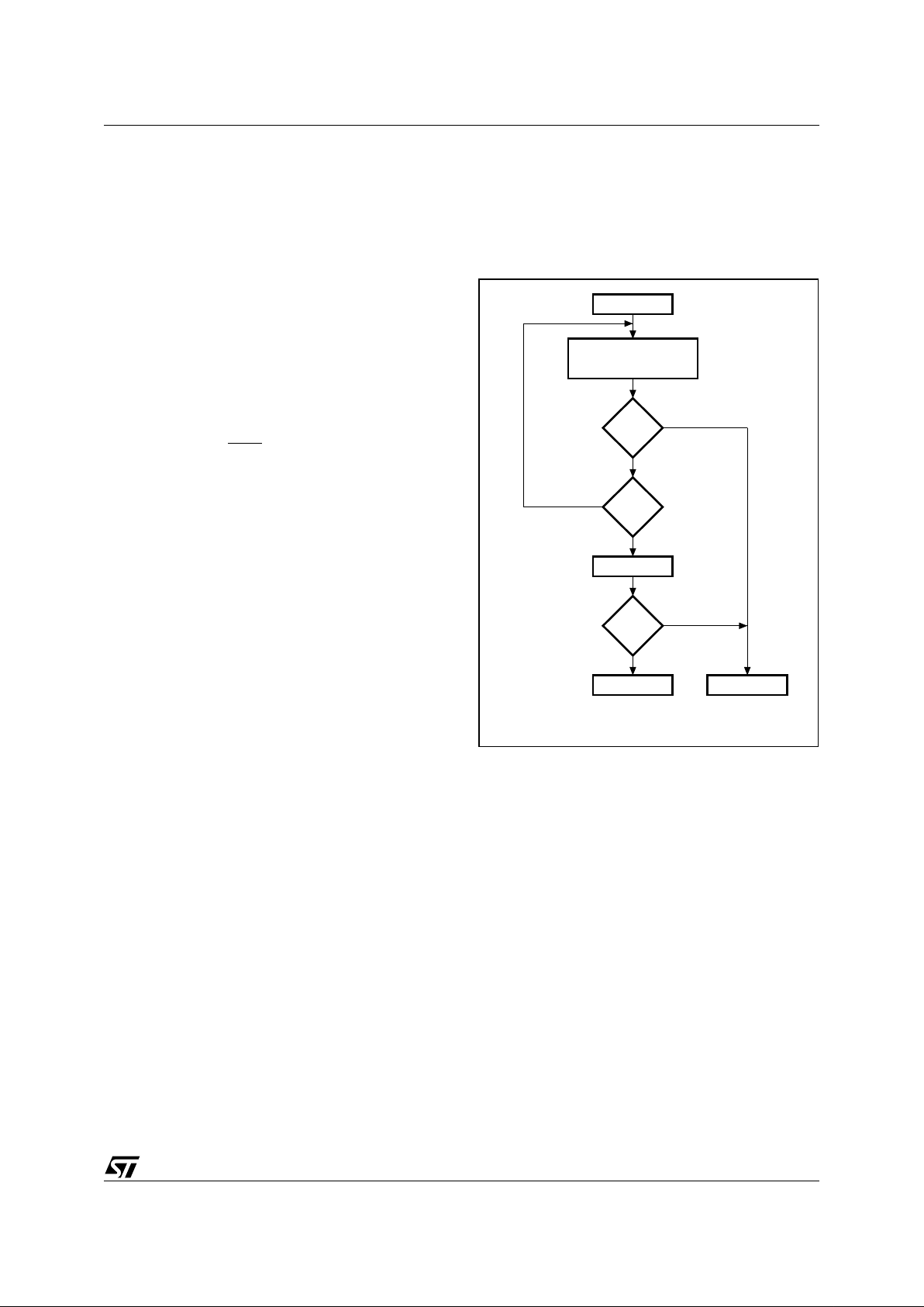
(DQ7) bit is a method of checking whether a Program or Erase cycle is in progress or has completed. Figure 4 shows the Data Polling algorithm.
When the MCU issue s a Program ins truction, the
embedded algorithm within the PSD begins. The
MCU then reads the location of the byte to be programmed in Flash memory to check status. The
Data Polling Flag (DQ7) bit of this location becomes the complem ent of b7 of the original data
byte to be programmed. The MCU continues to
poll this location, comparing the Dat a Polling Fl ag
(DQ7) bit and monitoring the Error Flag (DQ5) bit.
When the Data Polling Flag (DQ7) bit matches b7
of the original data, and the E rror Flag (DQ5) bit
remains 0, the embedded algorithm is complete. If
the Error Flag (DQ5) bit is 1, the MCU should test
the Data Polling Flag (DQ7) bit again since the
Data Polling Flag (DQ7) bit may have changed simultaneously with the Error Flag (DQ5) bit (see
Figure 4).
The Error Flag (DQ5) bit is set if either an internal
time-out occurred while the embedded algorithm
attempted to program the byte or if the MCU a ttempted to program a 1 to a bit that was not erased
(not erased is logic 0).
It is suggested (as with all Flash memories) to read
the location again after the embedded programming algorithm has completed, to compare the
byte that was written to the Flash memory with the
byte that was intended to be written.
When using the Data Polling method during an
Erase cycle, Figure 4 still applies. However, the
Data Polling Flag (DQ7) bit is 0 until the Erase cycle is complete. A 1 on the Error Flag (DQ5) bit indicates a time-out condition on the Erase cycle; a
0 indicates no error. The MCU can read any loca-
tion within the sector being erased to get the Data
Polling Flag (DQ7) bit and the Error Flag (DQ5) bit.
PSDsoft Express generates ANSI C code functions which implement these Data Polling algorithms.
Figure 4. Dat a Po ll i ng F lo wc h a rt
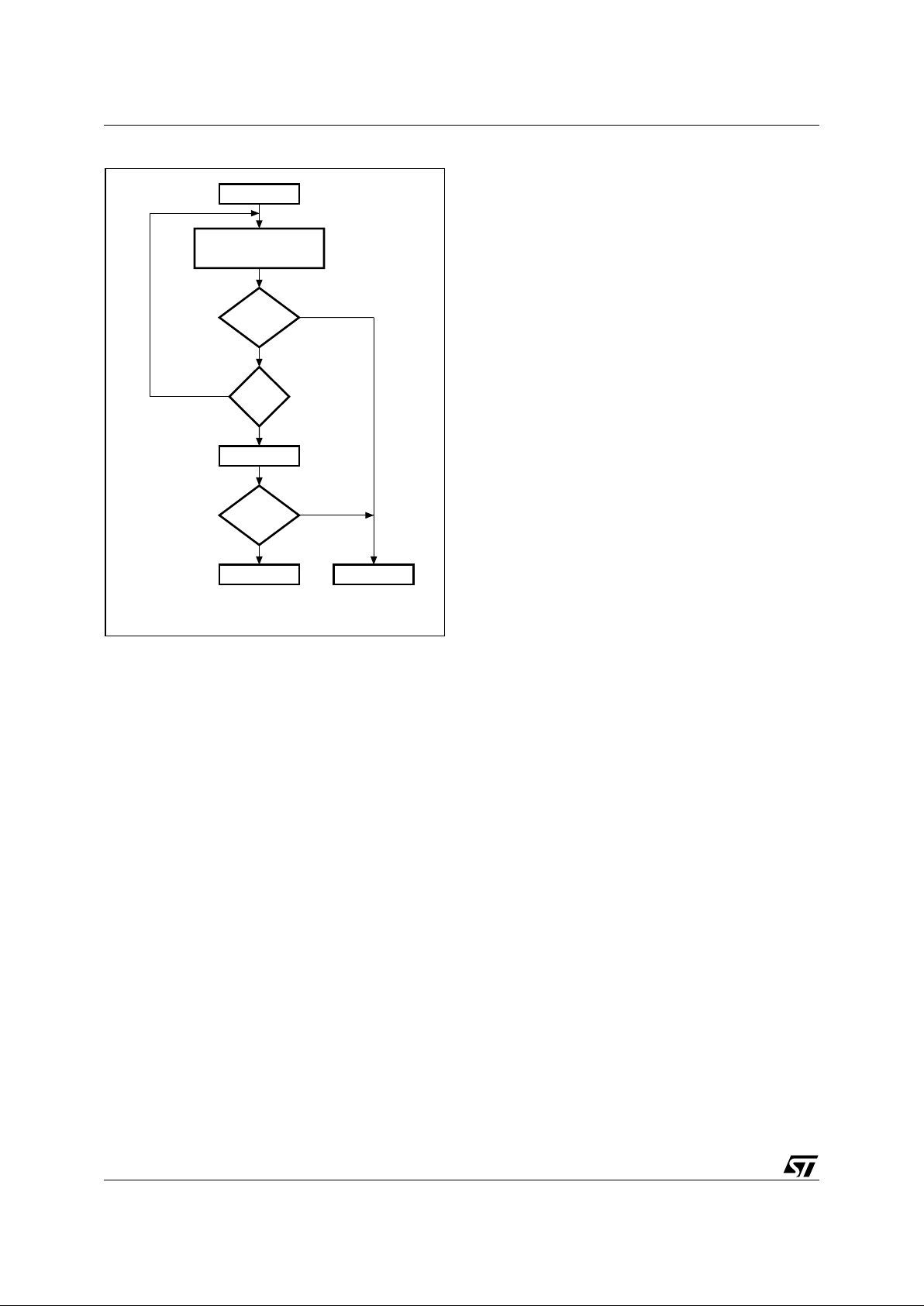
Data Toggle. Checking the Toggle Flag (DQ6) bit
is a method o f det erm ining whether a Pr ogram or
Erase cycle is in progress or has completed. Figure 5 shows the Data Toggle algorithm.
When the MCU issue s a Program ins truction, the
embedded algorithm within the PSD begins. The
MCU then reads the location of the byte to be programmed in Flash memory to check status. The
Toggle Flag (DQ6) bit of this location toggles each
time the MCU reads this location until the embedded algorithm is complete. The MCU cont inues t o
read this location, checking the Toggle Flag (DQ6)
bit and monitoring the Error Flag (DQ5) bit. When
the Toggle Flag (DQ6) bit stops toggling (two consecutive reads yield the same value), and the Error Flag (DQ5) bit remains 0, the embedded
algorithm is complete. If the Error Flag (DQ5) bit is
1, the MCU should test the Toggle Flag (DQ6) bit
again, since the Toggle Flag (DQ6) bit may have
changed simultaneously with the Error Flag (DQ5)
bit (see Figure 5).
READ DQ5 & DQ7
at VALID ADDRESS
START
READ DQ7
FAIL PASS
AI01369B
DQ7
=
DATA
YES
NO
YES
NO
DQ5
= 1
DQ7
=
DATA
YES
NO
PSD834F2V
20/89
Figure 5. Dat a Toggle Flow cha rt
The Error Flag (DQ5) bit is set if either an internal
time-out occurred while the embedded algorithm
attempted to program the byte, or if the MCU attempted to program a 1 to a bit that was not erased
(not erased is logic 0).
It is suggested (as with all Flash memories) to read
the location again after the embedded programming algorithm has completed, to compare the
byte that was written to Flash memory with the
byte that was intended to be written.
When using the Data Toggle method after an
Erase cycle, Figure 5 still applies. the Toggle Flag
(DQ6) bit toggles until the Erase cycle is complete.
A 1 on the Error Flag (DQ5) bit indicates a time-out
condition on the Erase cycle; a 0 indicates no error. The MCU can read any location within the sector being erased to get the To ggle Flag (DQ 6) bit
and the Error Flag (DQ5) bit.
PSDsoft Express generates ANSI C code functions which implement these Data T oggling algorithms.
Unlock Bypass. The Unlock Bypass instructions
allow the system to program bytes to the Flash
memories faster than using the standard Program
instruction. The Unloc k Bypass mode is ent ered
by first initiati ng two Unlo ck cycles. T his is fol lowed
by a third Write cycle cont aining the Unlock Bypass code, 20h (as shown in Table 7).
The Flash memory then enters the Unlock Bypass
mode. A two-cycle Unlock Bypass Program instruction is all that is required t o program in this
mode. The first cycle in this instruction contains
the Unlock Bypass Program code, A0h. The second cycle contains the program address and data.
Additional data is programmed in t he same manner. These instructions dispense with the initial
two Unlock cycles required in the standard Program instruction, resulting in faster total Flash
memory programming.
During the Unlock Bypass mode, only the Unlock
Bypass Program and Unlock Bypass Reset Flash
instructions are valid.
To exit th e Un l o ck Bypass mode, the system must
issue the t wo-cycl e Unl ock Bypass Reset Fl ash i nstruction. The first cycle must contain the data
90h; the second cycle the data 00h. Addresses are
Don’t Care for both cycles. The Flash memory
then returns to Read mode.
Erasing Flash Memory
Flash Bulk Erase. The Flash Bulk Erase instruc-
tion uses six Write operat ion s followed by a Read
operation of the status register, as described in
Table 7. If any byte of the Bulk Erase instruction is
wrong, the Bulk Erase instruction aborts and the
device is reset to the Read Flash memory status.
During a Bulk Erase, the memory status may be
checked by reading the Error Flag (DQ5) bit, the
Toggle Flag (DQ6) bi t, and the Dat a Polling Flag
(DQ7) bit, as detailed in the section entitled “Programming Flash Memory”, on page 19. The Error
Flag (DQ5) bit returns a 1 if there has been an
Erase Failure (maximum number of Erase cycles
have been executed).
It is not necessary to program the memory with
00h because the PSD automatically does this before erasing to 0FFh.
During execution of the Bulk Erase instruction, the
Flash memory does not accept any instructions.
Flash Sector Erase. The Sector Erase instruction uses six Write operations, as described in Table 7. Additional Flash Sector Erase codes and
Flash memory sector addresses can be written
subsequently to erase other Flash memory sectors in parallel, without further coded cycles, if the
additional bytes are transm itted in a shorter time
than the time-out period of about 100 µs. The input
of a new Sector Erase code restarts the time-out
period.
The status of the internal timer can be monitored
through the level of the Erase Time-out Flag (DQ3)
bit. If the Erase Time-out Flag (DQ3) bit is 0, the
Sector Erase instruction has been received and
the time-out period is counting. If the Er ase Timeout Flag (DQ3) bit is 1, the time-out period has expired and the PSD is busy erasing the Flash mem-
READ
DQ5 & DQ6
START
READ DQ6
FAIL PASS
AI01370B
DQ6
=
TOGGLE
NO
NO
YES
YES
DQ5
= 1
NO
YES
DQ6
=
TOGGLE

21/89
PSD834F2V
ory sector(s). Before and d uring Erase time-out,
any instruction other than Suspend S ector Erase
and Resume Sector Erase instructions abort the
cycle that is currently in progress, and reset the
device to Read mode. It is not necessary to program the Flash memory sector with 00h as the
PSD does this automatically before erasing
(byte=FFh).
During a Sector Erase, the memory status may be
checked by reading the Error Flag (DQ5) bit, the
Toggle Flag (DQ6) bi t, and the Dat a Polling Flag
(DQ7) bit, as detailed in the section entitled “Programming Flash Memory”, on page 19.
During execution of the Erase cycle, the Flash
memory accepts only Reset and Suspend Sector
Erase instructions. Erasure of one Flash memory
sector may be suspended, in order to read data
from another Flash memory sector, and t hen resumed .
Suspend Sector Erase. When a Sector Erase
cycle is in progress, the Suspend Sector Erase instruction can be used to suspend the cycle by writing 0B0h to any address when an appropriate
Sector Se lect (FS0 -FS7 or CSBO OT0-CSBOOT3 )
is High. (See Table 7). This allows reading of data
from another Flash memory sector after the Erase
cycle has been suspended. Suspend Sector
Erase is accepted only during an E rase c ycle and
defaults to Read mode. A Suspe nd Sector Erase
instruction executed during an Erase time-out pe-
riod, in addition to suspending the Erase cycle, terminates the time out period.
The Toggle Flag (DQ6) bit stops toggling when the
PSD internal logic is suspended. The status of this
bit must be monitored at an address within the
Flash memory sector being erased. The Toggle
Flag (DQ6) bit stops toggling between 0.1 µs and
15 µs after the Suspend Sector Erase instruction
has been executed. The PSD is then automatically
set to Read mode.
If an Suspend Sector Erase instruction was executed, the following rules apply:
– Attempting to read from a Flash memory sector
that was being erased outputs invalid data.
– Reading from a Flash sector that was
not
being
erased is valid.
– The Flash memory
cannot
be programmed, and
only responds to Resume Sector Erase and Reset Flash instructions (Read is an operation and
is allowe d) .
– If a Reset Flash instruction is received, data in
the Flash memory sector that was being erased
is invalid .
Resume Sector Erase. If a Suspend Sector
Erase instruction was previously executed, the
erase cycle may be resumed with this instruction.
The Resume Sector Eras e instruction consists of
writing 030h to any address w hile an appropriate
Sector Se lect (FS0 -FS7 or CSBO OT0-CSBOOT3 )
is High. (See Table 7.)
PSD834F2V
22/89
Specific Features
Flash Memory Sector Protect. Each primary
and secondary Flash memory sector can be separately protected against Program and Erase cycles. Sector Protection provides additional data
security because it disables all Program or Erase
cycles. This mode can be activated through the
JTAG Port or a Device Programmer.
Sector protection can be selected for each sector
using the PSDsoft Express Configuration program. This automatically protects selected sectors
when the device is programmed through the JTAG
Port or a Device Programmer. Flash memory sec-
tors can be unprotected to allow updating of their
contents using the JTAG Port or a Device Programmer. The MCU can read (but cannot change)
the sector protection bits.
Any attempt to program or erase a protected Flash
memory sector is ignored by the device. The Verify
operation results in a read of the protected data.
This allows a guarantee of the retention of the Protection status.
The sector protection status can be read by the
MCU through the Flash memory protection and
PSD/EE protection registers (in the CSIOP block).
See Table 9 and Table 10.
Table 9. Sector Protection/Security Bit Definition – Flash Protection Register
Note: 1. Bit Defin it i ons:
Sec<i>_Prot 1 = Primary Flash memory or secondary Flash memory Sector <i> is write protected.
Sec<i>_Prot 0 = Primary Flas h m em ory or secondary Flash mem ory Sector <i> is not write prot ected.
Table 10. Sector Protection/Security Bit Definition – PSD/EE Protection Register
Note: 1. Bit Defin it i ons:
Sec<i>_Prot 1 = Secondary Flash memory Sector <i> is write protected.
Sec<i>_Prot 0 = Secondary Flash memory Sector <i> is not write protected.
Security_Bit 0 = Securi ty Bit in dev i ce has not been set.
1 = Security Bi t in device has been set.
Bit 7 Bit 6 Bit 5 Bit 4 Bit 3 Bit 2 Bit 1 Bit 0
Sec7_Prot Sec6_Prot Sec5_Prot Sec4_Prot Sec3_Prot Sec2_Prot Sec1_Prot Sec0_Prot
Bit 7 Bit 6 Bit 5 Bit 4 Bit 3 Bit 2 Bit 1 Bit 0
Security_Bit not used not used not used Sec3_Prot Sec2_Prot Sec1_Prot Sec0_Prot

23/89
PSD834F2V
Reset Flash. The Reset Flash instruction con-
sists of one Write cycle (see Table 7). It can also
be optionally preceded by the standard two write
decoding cycles (writing AAh to 555h and 55 h to
AAAh). It must be executed after:
– Reading the Flash Protection Status or Flash ID
– An Error condition has occurred (and the device
has set the Error Flag (DQ5) bit to 1) during a
Flash memory Program or Erase cycle.
The Reset Flash instruction puts the Flash memory back into normal Read mode. If an Error condition has occurred (and the device has set the Error
Flag (DQ5) bit to 1) the Flash memo ry is put back
into normal Read mode within 25 µ s of the Reset
Flash instruction having been issued. The Reset
Flash instruction is ignored when it is issued during a Program or Bulk Erase cycle of the Flash
memory. The Reset Flash instruction aborts any
on-going Sector Erase cycle, and returns the
Flash memory to the normal Read mode within
25 µs.
Reset (RESET
) Signal. A pulse on Reset (RE-
SET) aborts any cycle that is in progress, and resets the Flash memory to the Read mode. When
the reset occurs during a Program or Erase cycle,
the Flash memory takes up to 25 µ s to retur n to
the Read mode. It is recommended that the Reset
(RESET
) pulse (except for Power On Reset, as
described on page 60) be at least 25 µs so that the
Flash memory is always ready for the MCU to
fetch the bootstrap instructions after the Reset cycle is complete.
SRAM
The SRAM i s enabled when SR AM Select (RS0)
from the DPLD is High. SRAM Select (RS0) can
contain up to two prod uct terms, allow ing flexible
memory mapping.
The SRAM can be backed up usin g an external
battery. The external battery should be connected
to Voltage Stand-by (VSTBY, PC2). If you have an
external battery connected to the P SD, the contents of the SRAM are reta ined in the event of a
power loss. The contents of the SRAM are retained so long as the battery voltage remains at
2 V or greater. If the supply voltage falls below the
battery voltage, an internal power switch-over to
the battery occurs.
PC4 can be configured as an output that indicates
when power is being drawn from the external ba t-
tery. Battery-on Indicator (VBATON, PC4) is High
with the supply voltage falls below the battery voltage and the battery on Voltage Stand-by (VSTBY,
PC2) is supplying power to the internal SRAM.
SRAM Select (RS0), Voltage Stand-by (VSTBY,
PC2) and Battery-on Indicator (VBATON, PC4)
are all configured using PSDsoft Express Configuration.
Sector Select and SRAM Select
Sector Select (FS0-FS7, CSBOOT0-CSBOOT3)
and SRAM Select (RS0) are all outputs of the
DPLD. They are setup by writing equations for
them in PSDabel. The f oll owing rules ap ply t o t he
equations for these signals:
1. Primary Flash memory and secondary Flash
memory Sector Select signals must
not
be larg -
er than the physical sector size.
2. Any primary Flash memory sect or must
not
be
mapped in the same memory space as another
Flash memory sector.
3. A secondary Flash m emory sect or must
not
be
mapped in the same memory space as another
secondary Flash memory sector.
4. SRAM, I/O, and Peripheral I/O spaces must
not
overlap.
5. A secondary Flash memory sector
may
overlap
a primary Flash memory sector. In case of overlap, priority is given to the secondary Flash
memory se c tor .
6. SRAM, I/O, and Peripheral I/O spaces
may
overlap any other memory sector. Priority is given to the SRAM, I/O, or Peripheral I/O.
Example. FS0 is valid when the address is in the
range of 8000h to BFFFh, CSBOOT0 is valid from
8000h to 9FFFh, and RS0 is valid from 8000 h to
87FFh. Any address in the range of RS0 always
accesses the SRAM. Any address in the range of
CSBOOT0 greater than 87FFh (and less than
9FFFh) automatically addresses seco ndary Flash
memory segment 0. Any address greater than
9FFFh accesses the primary Flash me mory segment 0. You can see that half of the primary Flash
memory segment 0 and one-fou rth of secondary
Flash memory segment 0 cannot be accessed in
this example. Also no te that an equation t hat defined FS1 to anywhere in the range of 8000h to
BFFFh would
not
be valid.
PSD834F2V
24/89
Figure 6. Priority Level of Memory and I/O
Components
Figure 6 shows the priority levels for all memory
components. Any component on a higher level can
overlap and has priority over any component on a
lower level. Components on the same level must
not
overlap. Level one has the highest priority and
level 3 has the lowest.
Memory Select Configuration for MCUs with
Separate Program and Data Spaces. The 8 031
and compatible family of MCUs, which includes
the 80C51, 80C151, 80C251, and 80C51XA, have
separate address spaces for Program memory
(selected using Program Select Enable (PSEN
,
CNTL2)) and Data memory (selected using Read
Strobe (RD
, CNTL1)). Any of the memories within
the PSD can reside in either space or both spaces.
This is controlled through manipulation of the VM
register that resides in the CSIOP space.
The VM register is set using PSDsof t Express to
have an initial value. It can subsequently be
changed by the MCU so that memory mapping
can be changed on-the-fly.
For example, you may wish to have SRAM and primary Flash memory in the Data space at Boot-up,
and secondary Flash memory in the Program
space at Boot-up, and later s wap t he primary and
secondary Flash memories. This is easily done
with the VM register by using PSDsoft Express
Configuration to configure it for Boot-up and having the MCU change it when desired.
Table 11 describes the VM Register.
Table 11. VM Register
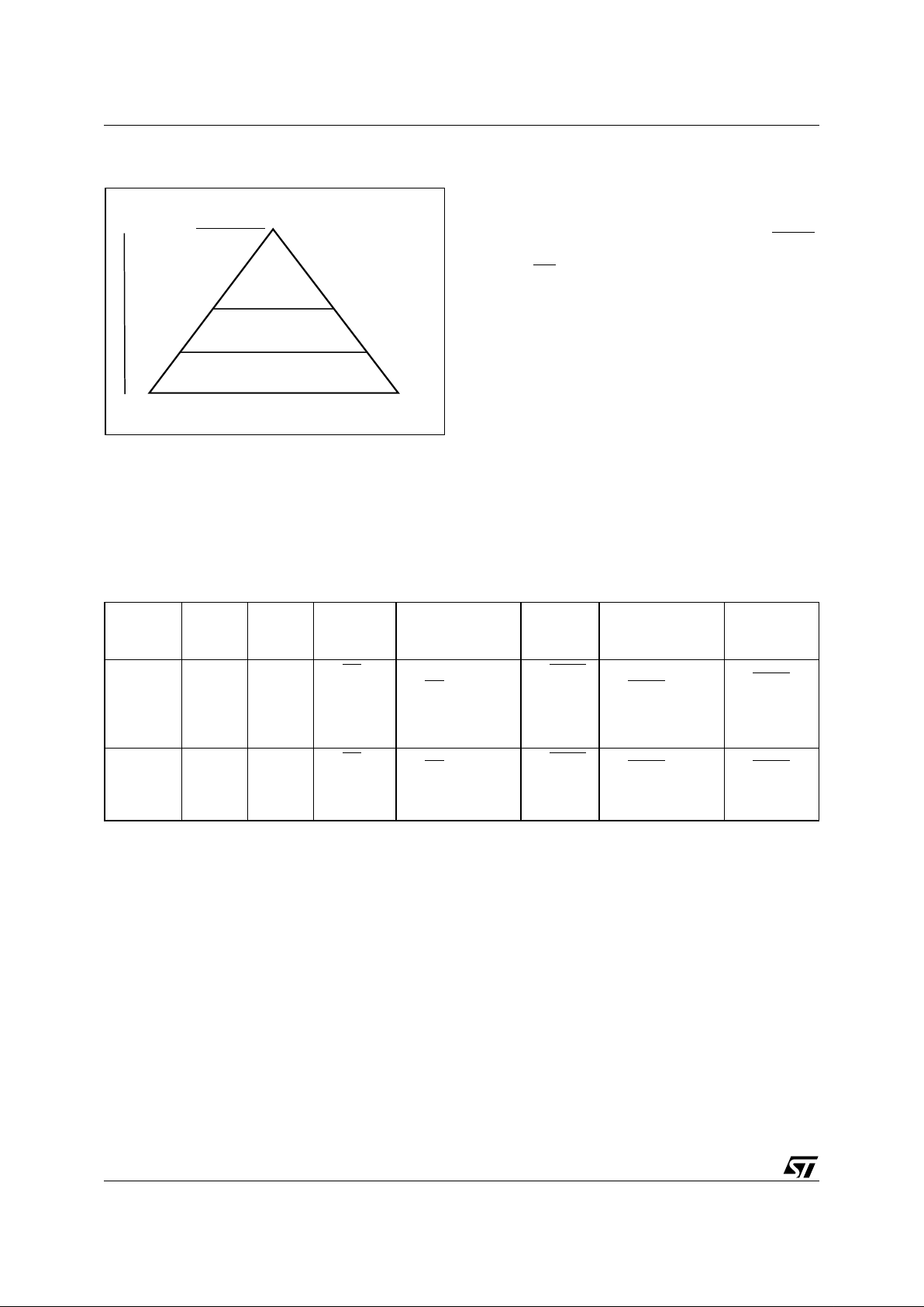
Level 1
SRAM, I/O, or
Peripheral I/O
Level 2
Secondary
Non-Volatile Memory
Highest Priority
Lowest Priority
Level 3
Primary Flash Memory
AI02867D
Bit 7
PIO_EN
Bit 6 Bit 5
Bit 4
Primary
FL_Data
Bit 3
Secondary
EE_Data
Bit 2
Primary
FL_Code
Bit 1
Secondary
EE_Code
Bit 0
SRAM_Code
0 = disable
PIO mode
not used not used
0 = RD
can’t
access
Flash
memory
0 = R
D can’t
access Secondary
Flash memory
0 = PSEN
can’t
access
Flash
memory
0 = PSE
N can’t
access Secondary
Flash memory
0 = PSEN
can’t
access
SRAM
1= enable
PIO mode
not used not used
1 = RD
access
Flash
memory
1 = R
D access
Secondary Flash
memory
1 = PSEN
access
Flash
memory
1 = PSE
N access
Secondary Flash
memory
1 = PSEN
access
SRAM
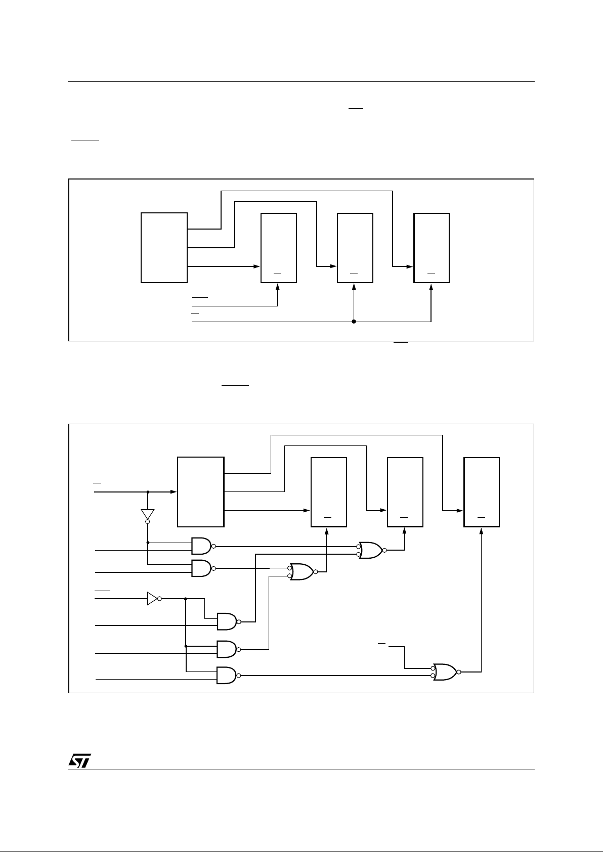
25/89
PSD834F2V
Configuration Modes for MCUs with Separate
Program and Data Spaces. Separate Space
Modes. Program space is separated from Data
space. For example, Program Select Enable
(PSEN
, CNTL2) is used to access the program
code from the primary Flash memory, while Read
Strobe (RD
, CNTL1) is used to access dat a from
the secondary Flash memory, SRAM and I/O Port
blocks. This configuration requires the VM register
to be set to 0Ch (see Figure 7).
Figure 7. 8031 Memory Modules – Separate Spac e
Combined Space Modes. The Program and
Data spaces are combined into one memory
space that allows the primary Flash memory, secondary Flash memory, and SRAM to be accessed
by either Program Select Enable ( PSEN
, CNTL2)
or Read Strobe (RD
, CNTL1). For example, to
configure the primary Flash mem ory in Combi ned
space, bits b2 and b4 of the VM register are set to
1 (see Figure 8).
Figure 8. 8031 Memory Modules – Combine d Space
Primary
Flash
Memory
DPLD
Secondary
Flash
Memory
SRAM
RS0
CSBOOT0-3
FS0-FS7
CS CSCS
OE OE
RD
PSEN
OE
AI02869C
Primary
Flash
Memory
DPLD
Secondary
Flash
Memory
SRAM
RS0
CSBOOT0-3
FS0-FS7
RD
CS CSCS
RD
OE OE
VM REG BIT 2
PSEN
VM REG BIT 0
VM REG BIT 1
VM REG BIT 3
VM REG BIT 4
OE
AI02870C
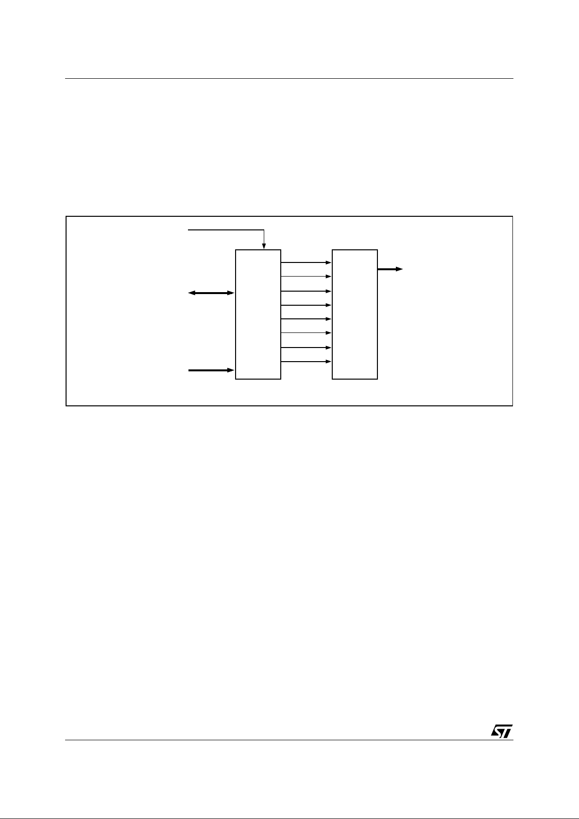
PSD834F2V
26/89
Page Re gi st er
The 8-bit Page Register increases the addressing
capability of the MCU by a factor of up to 256. The
contents of the register can also be read by the
MCU. The outputs of the Page Register (PGR0PGR7) are inputs to the DPLD decoder and can be
included in the Sector Select (FS0-FS7,
CSBOOT0-CSBOOT 3), and SRAM Select (RS0)
equations.
If memory paging is not needed, or if not all 8 page
register bits are needed for memory paging, then
these bits may be used in the CPLD for gen eral
logic. See Application Note
AN1154
.
Figure 9 shows the Page Regist er. The eight flipflops in the register are connected to the internal
data bus D0-D7. The MCU can write to or read
from the Page Register. The Page Register can be
accessed at address location CSIOP + E0h.
Figure 9. Page Re g ist er
RESET
D0-D7
R/W
D0 Q0
Q1
Q2
Q3
Q4
Q5
Q6
Q7
D1
D2
D3
D4
D5
D6
D7
PAGE
REGISTER
PGR0
PGR1
PGR2
PGR3
DPLD
AND
CPLD
INTERNAL
SELECTS
AND LOGIC
PLD
PGR4
PGR5
PGR6
PGR7
AI02871B
27/89
PSD834F2V
PLDS
The PLDs bring programmable logic f unctionality
to the PSD. After specifying the logic for the PLDs
using the PSDabel tool in PSDsoft Express, the
logic is programmed into the dev ice and av ailable
upon Power-up.
Table 12. DPL D a nd CP LD I nputs
Note: 1. The address inpu ts are A19-A4 in 80C51XA mode.
The PSD contains two PLDs: the Decode PLD
(DPLD), and the Complex PLD (CPLD). The PLDs
are briefly discussed in the next f ew paragraphs,
and in more detail in the sec tion entitled “Dec ode
PLD (DPLD)”, on page 29, and the section entitled
“Complex PLD (CPLD)”, also on page 30. Figure
10 shows the configuration of the PLDs.
The DPLD performs add ress decoding for Sel ect
signals for internal components, such as memory,
registers, and I/O ports.
The CPLD can be used for logic functions, such as
loadable counters and shift registers, state machines, and encoding and decoding logic. These
logic functions can be constructed using the 16
Output Macrocells (OMC), 24 Input Macrocells
(IMC), and the AND Array. The CPLD can also be
used to generate External Chip Select (ECS0ECS2) signals.
The AND Array is used to form product terms.
These product terms are specified using PSDabel.
An Input Bus consisting of 73 signals is connected
to the PLDs. The signals are shown in Table 12.
The Turbo Bit i n PSD
The PLDs in the PSD c an minimize power consumption by switching off when inputs remain unchanged for an extended time of about 70 ns.
Resetting the Turbo bit to 0 (Bit 3 of PMMR0) automatically places the PLDs into standby if no inputs are changing. Turning the Turbo mode off
increases propagation delays while reducing power consumption. See the section entitled “Power
Management”, on page 55, on how to set the Turbo bit.
Additionally, five bits are available in PMMR2 to
block MCU control signals from entering the PLDs.
This reduces power consumption and can be used
only when these MCU control signals are not used
in PLD logic equations.
Each of the two PLDs has unique characteristics
suited for its applications. They are described in
the following sections.
Input Source Input Name
Number
of
Signals
MCU Address Bus
1
A15-A0 16
MCU Control Signals CNTL2-CNTL0 3
Reset RST
1
Power-down PDN 1
Port A Input
Macrocells
PA7-PA0 8
Port B Input
Macrocells
PB7-PB0 8
Port C Input
Macrocells
PC7-PC0 8
Port D Inputs PD2-PD0 3
Page Register PGR7-PGR0 8
Macrocell AB
Feedback
MCELLAB.FB7FB0
8
Macrocell BC
Feedback
MCELLBC.FB7FB0
8
Secondary Flash
memory Program
Status Bit
Ready/Busy
1

PSD834F2V
28/89
Figure 10. PLD Diagram
PLD INPUT BUS
8
INPUT MACROCELL & INPUT PORTS
DIRECT MACROCELL INPUT TO MCU DATA BUS
CSIOP SELECT
SRAM SELECT
SECONDARY NON-VOLATILE MEMORY SELECTS
DECODE PLD
PAGE
REGISTER
PERIPHERAL SELECTS
JTAG SELECT
CPLD
PT
ALLOC.
MACROCELL
ALLOC.
MCELLAB
MCELLBC
DIRECT MACROCELL ACCESS FROM MCU DATA BUS
24 INPUT MACROCELL
(PORT A,B,C)
16 OUTPUT
MACROCELL
I/O PORTS
PRIMARY FLASH MEMORY SELECTS
3
PORT D INPUTS
TO PORT A OR B
TO PORT B OR C
DATA
BUS
8
8
8
4
1
1
2
1
EXTERNAL CHIP SELECTS
TO PORT D
3
73
16
73
24
OUTPUT MACROCELL FEEDBACK
AI02872C

29/89
PSD834F2V
Decode PLD (DPLD)
The DPLD, shown in Figure 11, is used for decoding the address for internal and external com ponents. The DPLD can be used to generate the
following decode signals:
■ 8 Sector Select (FS0-FS7) signals for the
primary Flash memory (three product terms
each)
■ 4 Sector Select (CSBOOT0-CSBOOT3) signals
for the secondary Flash memory (three product
terms each)
■ 1 internal SRAM Select (RS0) signal (two
product terms)
■ 1 internal CSIOP Select (PSD Configuration
Register) signal
■ 1 JTAG Select signal (enables JTAG on Port C)
■ 2 internal Peripheral Select signals
(Peripheral I/O mode).
Figure 11. DPLD Logic Array
(INPUTS)
(24)
(8)
(16)
(1)
PDN (APD OUTPUT)
I/O PORTS (PORT A,B,C)
(8)
PGR0 -PGR7
(8)
MCELLAB.FB [7:0] (FEEDBACKS)
MCELLBC.FB [7:0] (FEEDBACKS)
A[15:0
]
*
(3)
(3)
PD[2:0] (ALE,CLKIN,CSI)
CNTRL[2:0
] (
READ/WRITE CONTROL SIGNALS)
(1)
(1)
RESET
RD_BSY
RS0
CSIOP
PSEL0
PSEL1
8 PRIMARY FLASH
MEMORY SECTOR SELECTS
SRAM SELECT
I/O DECODER
SELECT
PERIPHERAL I/O MODE
SELECT
CSBOOT 0
CSBOOT 1
CSBOOT 2
CSBOOT 3
FS0
FS7
3
3
3
3
3
3
3
3
3
3
3
3
2
JTAGSEL
AI02873D
FS1
FS2
FS3
FS6
FS5
FS4
1
1
1
1

PSD834F2V
30/89
Complex PLD (CPLD)
The CPLD can be used to implement system logic
functions, such as loadable counters and shift registers, system mailboxes, ha ndshaking protocols,
state machines, and random logic. The CPLD can
also be used to genera te three External C hip Select (ECS0-ECS2), routed to Port D.
Although External Chip Select (ECS0-ECS2) can
be produced by any Output Macrocell (OMC),
these th ree Ext er nal Chi p Sel ect (E CS0 -ECS2) o n
Port D do not consume any Output Macrocells
(OMC).
As shown in Figure 10, the CPLD has the following
blocks:
■ 24 Input Macrocells (IMC)
■ 16 Output Macrocells (OMC)
■ Macrocell Allocat o r
■ Product Term Allocator
■ AND Array capable of generating up to 137
product terms
■ Four I/O Ports.
Each of the blocks are described in the sections
that fo llow.
The Input Macrocells (IMC) and Output Macrocells
(OMC) are connected to the PSD internal data bus
and can be directly accessed b y the MCU. This
enables the MCU software to load data into the
Output Macrocells (OMC) or read data from both
the Input and Output Macrocells (IMC and OMC).
This feature allows efficient implementation of system logic and eliminat es the need to connec t the
data bus to the AND Array as required in most
standard PLD macrocell architectures.
Figure 12. Macrocell and I/O Port
I/O PORTS
CPLD MACROCELLS
INPUT MACROCELLS
LATCHED
ADDRESS OUT
MUX
MUX
MUX
MUX MUX
D
D
Q
Q
Q
G
D
QD
WR
WR
PDR
DATA
PRODUCT TERM
ALLOCATOR
DIR
REG.
SELECT
INPUT
PRODUCT TERMS
FROM OTHER
MACROCELLS
POLARITY
SELECT
UP TO 10
PRODUCT TERMS
CLOCK
SELECT
PR DI LD
D/T
CK
CL
Q
D/T/JK FF
SELECT
PT CLEAR
PT
CLOCK
GLOBAL
CLOCK
PT OUTPUT ENABLE (OE
)
MACROCELL FEEDBACK
I/O PORT INPUT
ALE/AS
PT INPUT LATCH GATE/CLOCK
MCU LOAD
PT PRESET
MCU DATA IN
COMB.
/REG
SELECT
MACROCELL
TO
I/O PORT
ALLOC.
CPLD
OUTPUT
TO OTHER I/O PORTS
PLD INPUT BUSPLD INPUT BUS
MCU ADDRESS / DATA BUS
MACROCELL
OUT TO
MCU
DATA
LOAD
CONTROL
AND ARRAY
CPLD OUTPUT
I/O PIN
AI02874

31/89
PSD834F2V
Output Ma c rocell (OMC)
Eight of the Output Macrocells (OMC) are connected to Ports A and B pins an d are named as
McellAB0-McellAB7. The other eight macrocells
are connected to Ports B and C pins and are
named as McellBC0-McellBC7. If an McellAB output is not assigned to a specific pin in PSDabel,
the Macrocell Allocator block assigns i t to either
Port A or B. The same is true for a McellBC output
on Port B or C. Table 13 shows the macrocells and
port assignment.
The Output Macrocell (OMC) architecture is
shown in Figure 13. As shown in the figure, there
are native product terms a vailable from the AND
Array, and borrowed product terms available (if
unused) from other Output Macrocells (OMC). The
polarity of the product term is controlled by the
XOR gate. The Out put Macrocell (OMC) can im-
plement either sequential logic, usin g the flip-flop
element, or combinatorial logic. The multiplexer
selects between the sequential or combinatorial
logic outputs. The multiplexer out put can drive a
port pin and has a feedback path to the AND Array
inputs.
The flip-flop in the Out put Mac rocell (OM C) block
can be configured as a D, T, JK, or SR type in the
PSDabel program. The flip-flop’s clock, preset,
and clear inputs may be driven from a product
term of the AND Array. Alternatively, CLKIN (PD1)
can be used for the clock input to the flip-flop. The
flip-flop is clocked on the rising edge of CLKIN
(PD1). The preset and clear are active High inputs.
Each clear input can use up to two product terms.
Table 13. Output Macrocell Port and Data Bit Assignments
Output
Macrocell
Port
Assignment
Native Product Terms
Maximum Borrowed
Product Terms
Data Bit for Loading or
Reading
McellAB0 Port A0, B0 3 6 D0
McellAB1 Port A1, B1 3 6 D1
McellAB2 Port A2, B2 3 6 D2
McellAB3 Port A3, B3 3 6 D3
McellAB4 Port A4, B4 3 6 D4
McellAB5 Port A5, B5 3 6 D5
McellAB6 Port A6, B6 3 6 D6
McellAB7 Port A7, B7 3 6 D7
McellBC0 Port B0, C0 4 5 D0
McellBC1 Port B1, C1 4 5 D1
McellBC2 Port B2, C2 4 5 D2
McellBC3 Port B3, C3 4 5 D3
McellBC4 Port B4, C4 4 6 D4
McellBC5 Port B5, C5 4 6 D5
McellBC6 Port B6, C6 4 6 D6
McellBC7 Port B7, C7 4 6 D7

PSD834F2V
32/89
Product Term A l lo ca tor
The CPLD has a Product Term Allocator. The PSDabel compiler uses the Product Term Allocator to
borrow and place produ ct terms from one m acrocell to another. The following list summarizes how
product terms are allocated:
■ McellAB0-McellAB7 all have three native
product terms and may borrow up to six more
■ McellBC0-McellBC3 all have four native product
terms and may borrow up to five more
■ McellBC4-McellBC7 all have four native product
terms and may borrow up to six more.
Each macrocell may only borrow product terms
from certain other macrocells. Product terms already in use by one macrocell are not available for
another macrocell.
If an equation requires more product terms than
are available to it, then “external” product terms
are required, which consume other Output Macrocells (OMC). If external product terms are used,
extra delay is added for the equation that required
the extra product terms.
This is called product term expansion. PSDsoft
Express performs this expansion as needed.
Loading and Reading the Output Macrocells
(OMC). The Output Macrocells (OMC) block oc-
cupies a memory location in the MCU address
space, as defined by the CSIOP block (see the
section entitled “I/O Ports”, on page 45). The flipflops in each of t he 16 Out put Macrocells (OMC)
can be loaded from the data bus by a MCU. Loading the Output Macrocells (OMC) with data from
the MCU takes priority over internal func tions. As
such, the preset, clear, and clock inputs to the flipflop can be overridden by the MCU. The ability to
load the flip-flops and read them back is useful in
such applications as loadable counters and shift
registers, mailboxes, and handshaking protocols.
Data can be loaded to the Output Macrocells
(OMC) on the trailing ed ge of Write Strobe (WR
,
CNTL0) (edge loading) or during the time that
Write Strobe (WR
, CNTL0) is active (level loading). The method of loading is specified in PSDsoft
Express Configuration.

33/89
PSD834F2V
Figure 13. CP LD Output Macrocell
PT
ALLOCATOR
MASK
REG.
PT CLK
PT
PT
PT
CLKIN
FEEDBACK
(
.FB
)
PORT INPUT
AND ARRAY
PLD INPUT BUS
MUX
MUX
POLARITY
SELECT
LD
IN
CLR
Q
PRDIN
COMB/REG
SELECT
PORT
DRIVER
INPUT
MACROCELL
I/O PIN
MACROCELL
ALLOCATOR
INTERNAL DATA BUS
D
[
7:0
]
DIRECTION
REGISTER
CLEAR
(
.RE
)
PROGRAMMABLE
FF
(
D/T/JK /SR
)
WR
ENABLE
(
.OE
)
PRESET
(
.PR
)
RD
MACROCELL CS
AI02875B

PSD834F2V
34/89
The OMC Mask Register. There is one Mask
Register for each of the two groups of eight Output
Macrocells (OMC). The Mask Registers can be
used to block the loading of data to individual Output Macrocells (OMC). The def ault value for the
Mask Registers is 00h, which allows loading of the
Output Macrocells (OMC). When a given bit in a
Mask Register is set to a 1, the MCU is blocked
from writing to the associated Ou tput Macrocells
(OMC). For example, suppose McellAB0McellAB3 are being used for a state machine. You
would not want a MCU write to McellAB to overwrite the state machine registers. Therefore, you
would want to load the Mask Register for McellAB
(Mask Macrocell AB) with the value 0Fh.
The Output Enable of the OMC. The Output
Macrocells (OMC) block can be connected to an I/
O port pin as a P LD output. The output enab le of
each port pin driver is controlled by a single product term from the AND Array, ORed with the Direction Register output. The pin is enabled upon
Power-up if no output enable equation is defined
and if the pin is declared as a PLD output in PSDsoft Express.
If the Output Macrocell (O MC) output is declared
as an internal node and not as a port pin output in
the PSDabel file, the port pin can be used for other
I/O functions. The internal node feedback can be
routed as an input to the AND Array.
Input Macrocells (IMC)
The CPLD has 24 Input Macrocells (IMC), one for
each pin on Ports A, B, and C. The architecture of
the Input Macrocells (IMC) is shown in Figure 14.
The Input Macrocells (IMC) are individually configurable, and can be used as a latch, register, or to
pass incoming Port signals prior to driving them
onto the PLD input bus. The outputs of the Input
Macrocells (IMC) can be read by the MCU through
the internal data bus.
The enable fo r the latch and clock f or the regi ster
are driven by a multiplexer whose inputs are a
product term from the CPLD AND Array or the
MCU Address Strobe (ALE/AS). Each product
term output is used to latch or clock four Input
Macrocells (IMC). Port inputs 3-0 can be controlled by one product term and 7-4 by another.
Configurations for the Input Macrocells (IMC) are
specified by equations written in PSDabel (see Application Note
AN1171
). Outputs of the Input Mac-
rocells (IMC) can be read by the MCU via the IMC
buffer. See the section entitled “I/O Ports”, on
page 45.
Input Macrocells (IMC) can use Address Strobe
(ALE/AS, PD0) to latch address bits higher than
A15. Any latched addresses are routed to the
PLDs as inputs.
Input Macrocells (IMC) are particularly usefu l with
handshaking communication applications where
two processors pass data back and forth through
a common mailbox. Figure 15 shows a typical configuration where the Master MCU writes to the Port
A Data Out Register. This, in turn, can be read by
the Slave MCU via the activation of the “SlaveRead” output enable product term.
The Slave can also write to the Port A Input Macrocells (IMC) and the Master can then read the Input Macrocells (IMC) directly.
Note that the “Slave-Read” and “Slave-Wr” signals
are product terms that are derived from the Slave
MCU inputs Read Strobe (RD
, CNTL1), Write
Strobe (WR
, CNTL0), and Slave_CS.

35/89
PSD834F2V
Figure 14. Input Macrocell
OUTPUT
MACROCELLS BC
AND
MACROCELL AB
PT
PT
FEEDBACK
AND ARRAY
PLD INPUT BUS
PORT
DRIVER
I/O PIN
INTERNAL DATA BUS
D
[
7:0
]
DIRECTION
REGISTER
MUX
MUX
ALE/AS
PT
Q
Q
D
D
G
LATCH
INPUT MACROCELL
ENABLE
(
.OE
)
D FF
INPUT MACROCELL
_
RD
AI02876B

PSD834F2V
36/89
Figure 15. Handshaking Communication Using Input Macrocells
MASTER
MCU
MCU-RD
MCU-RD
MCU-WR
SLAVE–WR
SLAVE–CS
MCU-WR
D
[
7:0
]
D
[
7:0
]
CPLD
DQ
QD
PORT A
DATA OUT
REGISTER
PORT A
INPUT
MACROCELL
PORT A
SLAVE–READ
SLAVE
MCU
RD
WR
AI02877C
PSD

37/89
PSD834F2V
MCU BUS INTERFACE
The “no-glue logic” MCU Bus Interface block c an
be directly connected to most popular MCUs and
their control signals. Key 8-bit MCUs, with their
bus types and control signals, are shown in Tab le
14. The interface type is specified using the PSDsoft Express Configuration.
PSD Interface to a Multiplexed 8-Bit Bus. Figure 16 shows an example of a system using a
MCU with an 8-bit multiplexed bus and a PSD. The
ADIO port on the PSD is connected directly to the
MCU address/data bus. Address Strobe (ALE/AS,
PD0) latches the address signals internally.
Latched addresses can be brought out to Port A or
B. The PSD drives the ADIO data bus only when
one of its internal resources is accessed and Read
Strobe (RD
, CNTL1) is active. Should the system
address bus exceed sixteen bits, Ports A, B, C, or
D may be used as additional address inputs.
Table 14. MCUs and their Control Signals
Note: 1. Unu sed CNTL2 p i n can be configured as CPL D input. Other unused pins (P C7, PD0, PA 3-0) can be configured fo r other I/O fu nc-
tions.
2. ALE/AS i nput is optional for MCU s with a non-m ul t iplexed bus
MCU
Data Bus
Width
CNTL0 CNTL1 CNTL2 PC7
PD0
2
ADIO0 P A3-PA0 PA7-P A3
8031 8 WR
RD PSEN
(Note 1)
ALE A0
(Note 1) (Note 1)
80C51XA 8 WR
RD PSEN
(Note 1)
ALE A4 A3-A0
(Note 1)
80C251 8 WR
PSEN
(Note 1) (Note 1)
ALE A0
(Note 1) (Note 1)
80C251 8 WR
RD PSEN
(Note 1)
ALE A0
(Note 1) (Note 1)
80198 8 WR
RD
(Note 1) (Note 1)
ALE A0
(Note 1) (Note 1)
68HC11 8 R/W
E
(Note
1
) (Note 1)
AS A0
(Note 1) (Note 1)
68HC912 8 R/W
E
(Note
1
)
DBE
AS A0
(Note
1
) (Note 1)
Z80 8 WR
RD
(Note 1) (Note 1) (Note 1)
A0 D3-D0 D7-D4
Z8 8 R/W
DS
(Note 1) (Note 1)
AS
A0
(Note
1
) (Note 1)
68330 8 R/W
DS
(Note 1) (Note 1)
AS A0
(Note 1) (Note 1)
M37702M2 8 R/W
E
(Note 1) (Note 1)
ALE A0 D3-D0 D7-D4

PSD834F2V
38/89
Figure 16. An Example of a Typical 8-bit Multiplexed Bus Interface
PSD Interface to a Non-Multiplexed 8-Bit Bus.
Figure 17 shows an example of a system using a
MCU with an 8-bit non-multiplexed bus and a
PSD. The ad dress bus is con nected to the ADI O
Port, and the data bus is connected to Port A. Port
A is in tri-state mode when the PSD is not accessed by the MCU. Should the system address bus
exceed sixteen bits, Ports B, C, or D may be used
for additional address inputs.
MCU
WR
RD
BHE
ALE
RESET
AD[7:0
]
A[15:8
]
A[15:8
]
A[7:0
]
ADIO
PORT
PORT
A
PORT
B
PORT
C
WR (CNTRL0
)
RD (CNTRL1
)
BHE (CNTRL2
)
RST
ALE (PD0
)
PORT D
(
OPTIONAL
)
(
OPTIONAL
)
PSD
AI02878C

39/89
PSD834F2V
Figure 17. An Example of a Typical 8-bit Non-Multiplexed Bus Interface
Data Byte Enable Reference. MCUs have differ-
ent data byte orientations. Table 15 shows how
the PSD interprets byte/word operations in different bus write configurations. Even-byte refers to
locations with address A0 equal to 0 and odd byte
as locations with A0 equal to 1.
Table 15. Eight-Bit Data Bus
Figure 18. MCU Bus Interface Examples
Figure 19 to Figure 22 show examples of the basic
connections between the PS D and some popular
MCUs. The PSD Control input pins are labeled as
to the MCU function for whi ch t hey are configured.
The MCU bus in terface i s s pecified us ing the PSDsoft Express Configuration.
80C31. Figure 19 shows the bus interfac e for t he
80C31, which has an 8-bit multiplexed address/
data bus. The lo wer address byte is multiplexed
with the data bus. T he MCU control signals Program Select Enable (PSEN
, CNTL2), Read Strobe
(RD
, CNTL1), and Write Strobe (WR, CNTL0) may
be used for accessing the internal m emory and I/
O Ports blocks. Address Strobe (ALE/AS, PD0)
latches the address.
MCU
WR
RD
BHE
ALE
RESET
D[7:0
]
A[15:0
]
A[23:16
]
D[7:0
]
ADIO
PORT
PORT
A
PORT
B
PORT
C
WR (CNTRL0
)
RD (CNTRL1
)
BHE (CNTRL2
)
RST
ALE (PD0
)
PORT D
(OPTIONAL)
PSD
AI02879C
BHE A0 D7-D0
X 0 Even Byte
X 1 Odd Byte

PSD834F2V
40/89
Figure 19. Interfacing the PSD with an 80C31
80C251. The Intel 80C251 MCU fea tures a user-
configurable bus interface with four possible bus
configurations, as shown in Table 16.
Table 16. 80C251 Configurations
EA/VP
X1
X2
RESET
RESET
INT0
INT1
T0
T1
P1.0
P1.1
P1.2
P1.3
P1.4
P1.5
P1.6
P1.7
P0.0
P0.1
P0.2
P0.3
P0.4
P0.5
P0.6
P0.7
PA0
PA1
PA2
PA3
PA4
PA5
PA6
PA7
PB0
PB1
PB2
PB3
PB4
PB5
PB6
PB7
PC0
PC2
PC1
PC3
PC4
PC5
PC6
PC7
P2.0
P2.1
P2.2
P2.3
P2.4
P2.5
P2.6
P2.7
ADIO0
ADIO1
ADIO2
ADIO3
ADIO4
ADIO5
ADIO6
ADIO7
ADIO8
ADIO9
ADIO10
ADIO11
ADIO12
ADIO13
ADIO14
ADIO15
CNTL0 (WR)
CNTL1(RD)
CNTL2(PSEN)
PD0-ALE
PD1
PD2
RESET
RD
WR
PSEN
ALE/P
TXD
RXD
RESET
29
28
27
25
24
23
22
21
30
39
31
19
18
9
12
13
14
15
1
2
3
4
5
6
7
8
38
37
36
35
34
33
32
AD0
AD1
AD2
AD3
AD4
AD5
AD6
AD7
AD0
AD1
AD2
AD3
AD4
AD5
AD6
AD7
31
32
33
34
35
36
37
39
40
41
42
43
44
45
46
47
48
50
49
10
9
8
7
6
5
4
3
2
52
51
PSD
80C31
AD7-AD0
AD[7:0
]
21
22
23
24
25
26
27
28
17
16
29
30
A8
A9
A10
A11
A12
A13
A14
A15
RD
WR
PSEN
ALE
11
10
RESET
20
19
18
17
14
13
12
11
AI02880C
Configuration 80C251 Read/Write Pins Connecting to PSD Pins Page Mode
1
WR
RD
PSEN
CNTL0
CNTL1
CNTL2
Non-Page Mode, 80C31
compatible A7-A0 multiplex with
D7-D0
2
WR
PSEN only
CNTL0
CNTL1
Non-Page Mode
A7-A0 multiplex with D7-D0
3
WR
PSEN only
CNTL0
CNTL1
Page Mode
A15-A8 multiplex with D7-D0
4
WR
RD
PSEN
CNTL0
CNTL1
CNTL2
Page Mode
A15-A8 multiplex with D7-D0

41/89
PSD834F2V
The first configuration is 80C31 compatible, and
the bus interface to the PSD is identical to that
shown in Figure 19. The second and third configurations have the same bus connection as shown in
Figure 17. There is only one Read Strobe (PSEN
)
connected to CNTL1 on the PSD. The A16 connection to PA0 allows for a larger address input to
the PSD. The fourth configuration is shown in Figure 20. Read Strobe ( RD
) is connected to CNTL1
and Program Select Enable (PSEN
) is connected
to CNTL2.
The 80C251 has two major operating modes:
Page mode and Non-page mode. In Non-page
mode, the data is multiplexed with the lower address byte, and Address Strobe (ALE/AS, PD0) is
active in every bus cycle. I n Page mo de, data (D7 D0) is multiplexed with address (A15-A8). In a bus
cycle where there is a P age hit, Address Strobe
(ALE/AS, PD0) is not act ive and only addresses
(A7-A0) are changing. The PSD supports both
modes. In Page Mode, the PSD bus timing is identical to Non-Page Mode except the address h old
time and setup time with respect to Address
Strobe (ALE/AS, PD0) is not required. The PSD
access time is measured from address (A7-A0)
valid to data in v alid .
Table 17. Interfacing the PSD with the 80C251, with One Read Input
Note: 1. The A 16 and A17 connections are optional.
2. In non-P age-Mode, AD 7-AD0 con nects to ADIO7-ADIO0.
ADIO0
ADIO1
ADIO2
ADIO3
ADIO4
ADIO5
ADIO6
ADIO7
ADIO8
ADIO9
ADIO10
ADIO11
ADIO12
ADIO13
ADIO14
ADIO15
CNTL0(WR
)
CNTL1(RD
)
CNTL2(PSEN)
PD0-ALE
PD1
PD2
RESET
32
26
43
42
41
40
39
38
37
36
24
25
27
28
29
30
31
33
A0
A1
A2
A3
A4
A5
A6
A7
AD8
AD9
AD10
AD14
AD15
AD13
AD11
AD12
A0
A1
A2
A3
A4
A5
A6
A7
AD8
AD9
AD10
AD11
AD15
ALE
WR
A16
RD
AD14
AD12
AD13
14
9
2
3
4
5
6
7
8
21
20
11
13
P1.0
P1.1
P1.2
P1.3
P1.4
P1.5
P1.6
P1.7
P3.0/RXD
P3.1/TXD
P3.2/INT0
X2
X1
P3.3/INT1
RST
EA
A16
1
P0.1
P0.0
P0.2
P0.3
P0.4
P0.5
P0.6
P0.7
P2.0
P2.1
P2.2
P2.3
P2.4
P2.5
P2.6
P2.7
ALE
PSEN
WR
RD/A16
PC0
PC1
PC3
PC4
PC5
PC6
PC7
19
18
30
31
32
33
34
35
36
37
39
40
41
42
43
44
45
46
48
8
9
10
49
50
47
29
28
27
25
24
23
22
21
20
19
18
17
14
13
12
11
PB0
PB1
PB2
PB3
PB4
PB5
PB6
PB7
PA0
PA1
PA2
PA3
PA4
PA5
PA6
PA7
7
6
5
4
3
2
52
51
80C251SB
PSD
RESET
RESET
35
P3.4/T0
P3.5/T1
16
15
17
10
RESET
PC2
AI02881C
A17
1

PSD834F2V
42/89
Figure 20. Interfacing the PSD with the 80C251, with R D and PSEN Inp uts
80C51XA. The Philips 80C51XA MCU family sup-
ports an 8- or 16-bit multiplexed bus that can have
burst cycles. Address bits (A3-A0) are not multiplexed, while (A19-A4) are multiplexed with data
bits (D15-D0) in 16-bit mode. In 8-bit mode, (A11A4) are multiplexed with data bits (D7-D0).
The 80C51XA can be configured to operate in
eight-bit data mode (as shown in Figure 21).
The 80C51XA improves bus throughput and performance by executing burst cycles for code f etch-
es. In Burst Mode, address A19-A4 are latched
internally by the PSD, while the 80C51XA changes
the A3-A0 signals to f etch up t o 16 by tes of code.
The PSD access time is then measured from address A3-A0 valid to data in valid. The PSD bus
timing requirement in Burst Mode is identical to the
normal bus cycle, except the address setup and
hold time with respect to Address Strobe (ALE/AS,
PD0) does not apply.
ADIO0
ADIO1
ADIO2
ADIO3
ADIO4
ADIO5
ADIO6
ADIO7
ADIO8
ADIO9
ADIO10
ADIO11
ADIO12
ADIO13
ADIO14
ADIO15
CNTL0(WR
)
CNTL1(RD
)
CNTL2(PSEN)
PD0-ALE
PD1
PD2
RESET
32
26
43
42
41
40
39
38
37
36
24
25
27
28
29
30
31
33
A0
A1
A2
A3
A4
A5
A6
A7
AD8
AD9
AD10
AD14
AD15
AD13
AD11
AD12
A0
A1
A2
A3
A4
A5
A6
A7
AD8
AD9
AD10
AD11
AD15
ALE
WR
PSEN
RD
AD14
AD12
AD13
14
9
2
3
4
5
6
7
8
21
20
11
13
P1.0
P1.1
P1.2
P1.3
P1.4
P1.5
P1.6
P1.7
P3.0/RXD
P3.1/TXD
P3.2/INT0
X2
X1
P3.3/INT1
RST
EA
P0.1
P0.0
P0.2
P0.3
P0.4
P0.5
P0.6
P0.7
P2.0
P2.1
P2.2
P2.3
P2.4
P2.5
P2.6
P2.7
ALE
PSEN
WR
RD/A16
PC0
PC1
PC3
PC4
PC5
PC6
PC7
19
18
30
31
32
33
34
35
36
37
39
40
41
42
43
44
45
46
48
8
9
10
49
50
47
29
28
27
25
24
23
22
21
20
19
18
17
14
13
12
11
PB0
PB1
PB2
PB3
PB4
PB5
PB6
PB7
PA0
PA1
PA2
PA3
PA4
PA5
PA6
PA7
7
6
5
4
3
2
52
51
80C251SB
PSD
RESET
RESET
35
P3.4/T0
P3.5/T1
16
15
17
10
RESET
PC2
AI02882C

43/89
PSD834F2V
Figure 21. Interfacing the PSD with the 80C51X, 8-bit Data Bus
68HC11. Figure 22 shows a bus interface to a
68HC11 where the PSD is configured in 8-bit multiplexed mode with E and R/W settings. The DPLD
can be used to generate the READ and WR signals for external devices.
ADIO0
ADIO1
ADIO2
ADIO3
AD104
AD105
ADIO6
ADIO7
ADIO8
ADIO9
ADIO10
ADIO11
AD1012
AD1013
ADIO14
ADIO15
CNTL0(WR
)
CNTL1(RD
)
CNTL2(PSEN)
PD0-ALE
PD1
PD2
RESET
31
33
36
2
3
4
5
43
42
41
40
39
38
37
24
25
26
27
28
29
30
A4D0
A5D1
A6D2
A7D3
A8D4
A9D5
A10D6
A11D7
A12
A13
A14
A18
A19
A17
A15
A16
A0
A1
A2
A3
A4D0
A5D1
A6D2
A7D3
A8D4
A9D5
A10D6
A11D7
A12
A16
A17
A18
A19
A15
A13
A14
TXD1
T2EX
T2
T0
RST
EA/WAIT
BUSW
A1
A0/WRH
A2
A3
A4D0
A5D1
A6D2
A7D3
A8D4
A9D5
A10D6
A11D7
A12D8
A13D9
A14D10
A15D11
A16D12
A17D13
A18D14
A19D15
PSEN
RD
WRL
PC0
PC1
PC3
PC4
PC5
PC6
PC7
ALE
PSEN
RD
WR
ALE
32
19
18
30
31
32
33
34
35
36
37
39
40
41
42
43
44
45
46
48
8
9
10
49
50
47
7
9
8
16
XTAL1
XTAL2
RXD0
TXD0
RXD1
21
20
11
13
6
29
28
27
25
24
23
22
21
20
19
18
17
14
13
12
11
PB0
PB1
PB2
PB3
PB4
PB5
PB6
PB7
PA0
PA1
PA2
PA3
PA4
PA5
PA6
PA7
7
6
5
4
3
2
52
51
A0
A1
A2
A3
80C51XA
PSD
RESET
RESET
35
17
INT0
INT1
14
10
15
PC2
AI02883C

PSD834F2V
44/89
Figure 22. Interfacing the PSD with a 68HC11
9
10
11
12
13
14
15
16
ADIO0
ADIO1
ADIO2
ADIO3
AD104
AD105
ADIO6
ADIO7
ADIO8
ADIO9
ADIO10
ADIO11
AD1012
AD1013
ADIO14
ADIO15
CNTL0(R_W)
CNTL1(E)
CNTL2
PD0–AS
PD1
PD2
RESET
20
21
22
23
24
25
3
5
4
6
42
41
40
39
38
37
36
35
AD0
AD0
AD1
AD2
AD3
AD4
AD5
AD6
AD7
A8
A9
A10
A14
A15
A13
A11
A12
AD1
AD2
AD3
AD4
AD5
AD6
AD7
E
AS
R/W
XT
EX
RESET
IRQ
XIRQ
PA0
PA1
PA2
PE0
PE1
PE2
PE3
PE4
PE5
PE6
PE7
VRH
VRL
PA3
PA4
PA5
PA6
PA7
PB0
PB1
PB2
PB3
PB4
PB5
PB6
PB7
PA0
PA1
PA2
PA3
PA4
PA5
PA6
PA7
PC0
PC1
PC2
PC3
PC4
PC5
PC6
PC7
PC0
PC1
PC3
PC4
PC5
PC6
PC7
PD0
PD1
PD2
PD3
PD4
PD5
MODA
E
AS
R/W
31
30
31
32
33
34
35
36
37
39
40
41
42
43
44
45
46
48
8
9
10
49
50
47
8
7
17
19
18
34
33
32
43
44
45
46
47
48
49
50
52
51
30
29
28
27
29
28
27
25
24
23
22
21
20
19
18
17
14
13
12
11
PB0
PB1
PB2
PB3
PB4
PB5
PB6
PB7
7
6
5
4
3
2
52
51
MODB
2
68HC11
PSD
RESET
RESET
AD7-AD0
AD7-AD0
PC2
AI02884C

45/89
PSD834F2V
I/O PO R T S
There are four programmable I/O ports: Ports A, B,
C, and D. Each of the ports is eight bits except Port
D, which is 3 bits. Each port pin is individually user
configurable, thus allowing multiple functions per
port. The ports are configured using PSDsoft Express Configuration or by the MCU writing to onchip registers in the CSIOP space.
The topics discussed in this section are:
■ General Port architect ur e
■ Port operating modes
■ Port Configuration Registers (PCR)
■ Port Data Registers
■ Individual Port functionality.
General Port Architecture
The general architecture of the I/O Port block is
shown in Figure 23. Individual Port architectures
are shown in Figure 25 to Figure 28. In general,
once the purpose for a port pin has been defined,
that pin is no longer available for other purposes.
Exceptions are noted.
As shown in Figure 23, the ports contain an output
multiplexer whose select signals are driven by the
configuration bits in the Control Registers (Ports A
and B only) and PSDsoft Express Confi guration.
Inputs to the multiplexer include the following:
■ Output data from the Data Out register
■ Latched address outputs
■ CPLD macrocell output
■ External Chip Select (ECS0-ECS2) from the
CPLD.
The Port Data Buffer (PDB) is a tri-state buffer that
allows only one source at a time to be read. The
Port Data Buffer (PDB) is connected to the Internal
Data Bus for feedback and can be read by the
MCU. The Data Out and macrocell outputs, Direction and Control Registers, and port pin input are
all connected to the Port Data Buffer (PDB).
Figure 23. General I/O Port A rchi tec ture
INTERNAL DATA BUS
DATA OUT
REG.
DQ
DGQ
DQ
DQ
WR
WR
WR
ADDRESS
MACROCELL OUTPUTS
ENABLE PRODUCT TERM (.OE
)
EXT CS
ALE
READ MUX
P
D
B
CPLD-INPUT
CONTROL REG.
DIR REG.
INPUT
MACROCELL
ENABLE OUT
DATA IN
OUTPUT
SELECT
OUTPUT
MUX
PORT PIN
DATA OUT
ADDRESS
AI02885

PSD834F2V
46/89
Table 18. Port Operating Modes
Note: 1. Can be multiple xed with other I/O functions.
Table 19. Port Operating Mode Settings
Note: 1. N/A = Not Applicable
2. The direction of the Port A,B,C, and D pins are controlled by the Direction Register ORed with the individual output enable product
term (.oe) fr om the CPLD AND Array.
3. Any of thes e three methods enables the JTAG pin s on Port C.
Port Mode Port A Port B Port C Port D
MCU I/O Yes Yes Yes Yes
PLD I/O
McellAB Outputs
McellBC Outputs
Additional Ext. CS Outputs
PLD Inputs
Yes
No
No
Yes
Yes
Yes
No
Yes
No
Yes
No
Yes
No
No
Yes
Yes
Address Out Yes (A7 – 0)
Yes (A7 – 0)
or (A15 – 8)
No No
Address In Yes Yes Yes Yes
Data Port Yes (D7 – 0) No No No
Peripheral I/O Yes No No No
JTAG ISP No No
Yes
1
No
Mode
Defined in
PSDabel
Defined in PSD
Configura tion
Control
Register
Setting
Direction
Register
Setting
VM
Register
Setting
JTAG Enable
MCU I/O Declare pins only
N/A
1
0
1 = output,
0 = input
(Note
2
)
N/A N/A
PLD I/O Logic equations N/A N/A
(Note
2
)
N/A N/A
Data Port (Port A) N/A Specify bus type N/A N/A N/A N/A
Address Out
(Port A,B)
Declare pins only N/A 1
1 (Note
2
)
N/A N/A
Address In
(Port A,B,C,D)
Logic for equation
Input Macrocells
N/A N/A N/A N/A N/A
Peripheral I/O
(Port A)
Logic equations
(PSEL0 & 1)
N/A N/A N/A PIO bit = 1 N/A
JTAG ISP (Note
3
)
JTAGSEL
JTAG
Configuration
N/A N/A N/A JTAG_Enable

47/89
PSD834F2V
Table 20. I/O Port Latched Address Output Assignments
Note: 1. N/A = Not Applicable.
The Port pin’s tri-state output driver enable is controlled by a two input OR gate whose inputs come
from the CPLD AND Array enable product term
and the Direction Register. If the enable product
term of any of the Array outputs are not defined
and that port pin is not defined as a CPLD ou tput
in the PSDabel file, then the Direction Register has
sole control of the buffer that drives the port pin.
The contents of these registers can be altered by
the MCU. The Port Data Buffer (PDB) feedback
path allows the MCU to check t he contents of the
registers.
Ports A, B, and C have embedded Input Macrocells (IMC). The Input Macrocells (IMC) can be
configured as latches, registers, or direct inputs to
the PLDs. The latches and registers are clocked
by Address Strobe (ALE/AS, PD0) or a product
term from the PLD AND Array. The outputs from
the Input Macrocells (IMC) drive the PLD input bus
and can be read by the MCU. See the section entitled “Input Macrocell”, on page 35.
Port Operat in g Mo des
The I/O Ports have several modes of operation.
Some modes can be defined using PSDabel,
some by the MCU writing to the Control Registers
in CSIOP space, and some by both. The modes
that can only be defined using PSDsoft Express
must be programmed into the device and cannot
be changed unless the device i s reprogrammed.
The modes that can be changed by the MCU can
be done so dynamically at run-time . The P LD I/O,
Data Port, Address Input, and Peripheral I/O
modes are the only modes that must be defined
before programming the device. A ll other modes
can be changed by the MCU at run-time. See Application Note
AN1171
for more detail.
Table 18 summarizes which mode s are available
on each port. Table 21 shows ho w and where the
different modes are configu red. Each of the port
operating modes are described in the following
sections.
MCU I/O Mode
In the MCU I/O mode, the MCU uses the I/O Ports
block to expand its own I/O ports. By setting up the
CSIOP space, the ports on the PSD are mapped
into the MCU address space. The addresses of
the ports are listed in Table 6.
A port pin can be put into MCU I/O mode by writing
a 0 to the corresponding bit in the Control Register. The MCU I/O direction may be changed by
writing to the corresponding bit in the Direction
Register, or by the output enable product term.
See the section entitled “Peripheral I/O Mode”, on
page 48. When the pin is configured as an output,
the content of the Data Out Register drives the pin.
When configured as an input, the MCU can read
the port input through the Data In buf fer . See Figure 23.
Ports C and D do not have Control Registers, and
are in MCU I/O mode by default. They can be used
for PLD I/O if equations are written for them in PSDabel.
PLD I/ O Mode
The PLD I/O Mode uses a po rt as an input to the
CPLD’s Input Macrocells (IMC), and/ or as an output from the CPLD’s Output Macrocells (OMC).
The output can be tri-stated with a control signal.
This output enable control signal can be d efined
by a product term from the PLD, or by resetting the
corresponding bit in the Direction Register to 0.
The corresponding bit in the Direction Register
must not be set to 1 if the pin is defined for a PLD
input signal in PSDabel. The PLD I/O mode is
specified in PSDabel by declaring the port pins,
and then writing an equ ation assigning the PLD I/
O to a port.
Address Out Mode
For MCUs with a multiplexed address/data bus,
Address Out Mode can be u sed to drive latched
addresses on to the port pins. These port pins can,
in turn, drive external devices. Either the output
enable or the corresponding bits of both the Direction Register and Control Register must be set to
a 1 for pins to use Address Out Mode. This m ust
be done by the MCU at run-time. See Table 20 for
the address output pin assignments on Ports A
and B for various MCUs.
MCU Port A (PA3-PA0) Port A (PA7-PA4) Port B (PB3-PB0) Port B (PB7-PB4)
8051XA (8-Bit)
N/A
1
Address a7-a4 Address a11-a8 N/A
80C251
(Page Mode)
N/A N/A Address a11-a8 Address a15-a12
All Other
8-Bit Multiplexed
Address a3-a0 Address a7-a4 Address a3-a0 Address a7-a4
8-Bit
Non-Multiplexed Bus
N/A N/A Address a3-a0 Address a7-a4

PSD834F2V
48/89
For non-multiplexed 8-bit bus mode , address s ignals (A7-A0) are available to Port B in Address Out
Mode.
Note: Do not d rive address signals with A ddress
Out Mode to an external mem ory de vice if it is intended for the MCU to Boot from the external device . The M CU mu st fi rs t B oot fro m PS D me mor y
so the Direction and Control register bits can be
set .
Address In Mode
For MCUs that have more than 16 address signals, the higher addresses can be connected t o
Port A, B, C, and D. The address input can be
latched in the Input Macrocell (IMC) by Address
Strobe (ALE/AS, PD0). Any input that is included
in the DPLD equations for the SRAM, or primary or
secondary Flash memory is considered to be an
address input.
Data Port Mode
Port A can be used as a data bus port for a MCU
with a non-multiplexed address/data bus. The
Data Port is connected to the data bus of the MCU.
The general I/O functions a re disabl ed in Po rt A if
the port is configured as a Data Port.
Peripheral I/O Mode
Peripheral I/O mode can be used to interface with
external peripherals. In this mode, all of Port A
serves as a tri-state, bi-directional data buffer for
the MCU. Peripheral I/O Mode is enabled by setting Bit 7 of the VM Register to a 1. Figure 24
shows how Port A acts as a bi-directional buffer for
the MCU data bus if Peripheral I/O Mode is enabled. An equation for PSEL0 and/or PSEL1 must
be written in PSDabel. The buffer is tri-stated
when PSEL0 or PSEL1 is not active.
JTAG In-System Programmi ng (ISP)
Port C is JTAG compliant, and can be used for InSystem Programming (ISP). You can multiplex
JTAG operations with other functions on Port C
because In-System Programming (ISP) is not performed in normal Operating mode. For more information on the JTA G Po rt, see the section ent itled
“Programming In-Circuit using the JTAG Serial Interface”, on page 61.
Port Configuration Registers (PCR)
Each Port has a set of Port Configuration Registers (PCR) used for configuration. The contents of
the registers can be accessed by the MCU through
normal read/write bus cycles at the addresses given in Table 6. The addresses in Table 6 are the offsets in hexadecimal from the base of the CSIOP
register.
The pins of a port are individually configurable and
each bit in the register controls its respective pin.
For example, Bit 0 in a register refers to Bit 0 of its
port. The three Port Configuration Registers
(PCR), shown in Table 21, are used for setting the
Port configurations. The default Power-up state for
each register in Table 21 is 00h.
Table 21. Port Configuration Registers (PCR)
Note: 1. See T able 25 for Dri ve Register bit defini tion.
Control Register. Any bit reset to 0 in the Control
Register sets the corresponding port pin to MCU I/
O Mode, and a 1 sets it to Address Out Mode. The
default mode is MCU I/O. Only Ports A and B have
an associated Control Register.
Figure 24. Peripheral I/O Mode
Register Name Port M CU Access
Control A,B Write/Read
Direction A ,B,C,D Wr ite/Re ad
Drive Select
1
A,B,C,D Write/Read
RD
PSEL0
PSEL1
PSEL
VM REGISTER BIT 7
WR
PA0-PA7
D0-D7
DATA BUS
AI02886

49/89
PSD834F2V
Direction Register. The Direction Register, in
conjunction with the output enable (except for Port
D), controls the direction of data flow in the I/O
Ports. Any bit set to 1 in the Direction Register
causes the corresponding pin to be an output, and
any bit set to 0 causes it to be an input. The default
mode for all port pins is input.
Table 22. Port Pin Direction Control, Output
Enable P.T. Not Defined
Table 23. Port Pin Direction Control, Output
Enable P.T. Defined
Table 24. Port Direction Assignment Example
Figure 25 and Figure 26 s how the Port Architecture diagrams for Ports A/B and C, respectively.
The direction of data flow for Ports A, B, and C are
controlled not only by the direction register, but
also by the out put enable product term f rom the
PLD AND Array. If the output enable product term
is not active, the Direction Register has sole con-
trol of a given pin’s direction.
An example of a configuration for a Port with the
three least significant bits set to output and the remainder set to input is shown in Tab le 24. Since
Port D only contains three pins (shown i n Figure
28), the Direction Register for Port D has only the
three least significant bits active.
Drive Select Register. The Drive Select Register
configures the pin driver as Open Drain or CMOS
for some port pins, and controls the slew rate for
the other port pins. An external pull-up resistor
should be used for pins configured as Open Drain.
A pin can be configured as Open Drain if its corresponding bit in the Drive Select Register is set to a
1. The default pin drive is CMOS.
Note that the slew rate is a measurement o f the
rise and fall times of an output. A higher slew rate
means a faster output response and may create
more electrical noise. A pin operates in a high slew
rate when the corresponding bit in the Drive Register is set to 1. The default rate is slow slew.
Table 25 shows the Drive Register for Ports A, B,
C, and D. It summarizes which pins can be configured as Open Drai n outputs and which pins the
slew rate can be set for.
Port Data Registers
The Port Data Registers, shown in Table 26, are
used by the MCU to write data to or read data from
the ports. Table 26 sho ws the register name, the
ports having each register type, and MCU access
for each register type. The registers are described
below.
Table 25. Drive Register Pin Assignment
Note: 1. NA = Not Applicable.
Direction Register Bit Port Pin Mode
0 Input
1 Output
Direction
Register Bit
Output Enable
P.T.
Port Pin Mode
0 0 Input
0 1 Output
1 0 Output
1 1 Output
Bit 7 Bit 6 Bit 5 Bit 4 Bit 3 Bit 2 Bit 1 Bit 0
0 0 0 0 0 1 1 1
Drive
Register
Bit 7 Bit 6 Bit 5 Bit 4 Bit 3 Bit 2 Bit 1 Bit 0
Port A
Open
Drain
Open
Drain
Open
Drain
Open
Drain
Slew
Rate
Slew
Rate
Slew
Rate
Slew
Rate
Port B
Open
Drain
Open
Drain
Open
Drain
Open
Drain
Slew
Rate
Slew
Rate
Slew
Rate
Slew
Rate
Port C
Open
Drain
Open
Drain
Open
Drain
Open
Drain
Open
Drain
Open
Drain
Open
Drain
Open
Drain
Port D
NA
1
NA
1
NA
1
NA
1
NA
1
Slew
Rate
Slew
Rate
Slew
Rate

PSD834F2V
50/89
Table 26. Port Data Registers
Data In. Port pins are connected directly to the
Data In buffer. In MCU I/O inpu t mode, the pin input is read through the Data In buffer.
Data Out Register. Stores output data written by
the MCU in the MCU I/O output mode. The contents of the Register are driven out to the pins if the
Direction Register or the output enable product
term is set to 1. The contents of the register can
also be read back by the MCU.
Output Ma c rocells (OMC). The CPLD Output
Macrocells (OMC) occupy a location in the MCU’s
address space. The MCU can read the output of
the Output Macrocells (OM C). If the OMC Mask
Register bits are not set, writing to the macrocell
loads data to the macrocell flip-flops. See the section entitled “PLDs”, on page 27.
OMC Mask Register. Each OMC Mask Register
bit corresponds to an Output Macrocell (OMC) flipflop. When the OMC Mask Regi ster bit is set to a
1, loading data into the Output M acrocell (OMC)
flip-flop is blocked. The default value is 0 or unblocked.
Input Macrocells (IMC). The Input Macrocells
(IMC) can be used to latch or store external inputs.
The outputs of the Input Macrocells (IMC) are routed to the PLD in put bus, and c an be read by t he
MCU. See the section entitled “PLDs”, on page 27.
Enable Out. The Enable Out register can be read
by the MCU. It contains the output enable values
for a given port. A 1 indicates the driver is in output
mode. A 0 indicates the driver is in tri-state and the
pin is in input mode.
Register Name Port MCU Access
Data In A,B,C,D Read – input on pin
Data Out A,B,C,D Write/Read
Output Macrocell A,B,C
Read – outputs of macrocells
Write – loading macrocells flip-flop
Mask Macrocell A,B,C
Write/Read – prevents loading into a given
macrocell
Input Macrocell A,B,C Read – outputs of the Input Macrocells
Enable Out A,B,C Read – the output enable control of the port driver

51/89
PSD834F2V
Figure 25. Port A and Port B Structure
Ports A and B – Functionality and Structure
Ports A and B have similar functionality and structure, as shown in Figure 25. The two ports can be
configured to perform one or more of the following
functions:
■ MCU I/O Mode
■ CPLD Output – Macrocells McellAB7-McellAB0
can be connected to Port A or Port B. McellBC7McellBC0 can be connected to Port B or Port C.
■ CPLD Input – Via the Input Macrocells (IMC).
■ Latched Address output – Provide latched
address output as per Table 20.
■ Address In – Additional high address inputs
using the Input Macrocells (IMC).
■ Open Drain/Slew Rate – pins PA3-PA0 and
PB3-PB0 can be configured to fast slew rate,
pins PA7-PA4 and PB7-PB4 can be configured
to Open Drain Mode.
■ Data Port – Port A to D7-D0 for 8 bit non-
multiplexed bus
■ Multiplexed Address/Data port for certain types
of MCU bus interfaces.
■ Peripheral Mode – Port A only
INTERNAL DATA BUS
DATA OUT
REG.
DQ
DGQ
DQ
DQ
WR
WR
WR
ADDRESS
MACROCELL OUTPUTS
ENABLE PRODUCT TERM (.OE
)
ALE
READ MUX
P
D
B
CPLD- INPUT
CONTROL REG.
DIR REG.
INPUT
MACROCELL
ENABLE OUT
DATA IN
OUTPUT
SELECT
OUTPUT
MUX
PORT
A OR B PIN
DATA OUT
ADDRESS
A[7:0] OR A[15:8
]
AI02887

PSD834F2V
52/89
Figure 26. Port C Structure
Port C – Functionality and Structure
Port C can be configured to perform one or more
of the following functions (see Figure 26):
■ MCU I/O Mode
■ CPLD Output – McellBC7-McellBC0 outputs
can be connected to Port B or Port C.
■ CPLD Input – via the Input Macrocells (IMC)
■ Address In – Additional high address inputs
using the Input Macrocells (IMC).
■ In-System Programming (ISP) – JTAG port can
be enabled for programming/erase of the PSD
device. (See the section entitled “Programming
In-Circuit using the JTAG Serial Interface”, on
page 61, for more information on JTAG
programming.)
■ Open Drain – Port C pins can be configured in
Open Drain Mode
■ Battery Backup features – PC2 can be
configured for a battery input supply, Voltage
Stand-by (VSTBY).
PC4 can be configured as a Battery-on Indicator
(VBATON), indicating when V
CC
is less than
V
BAT
.
Port C does not support Address Out mode, and
therefore no Control Register is required.
Pin PC7 may be configured as the DBE input in
certain MCU bus interfaces.
INTERNAL DATA BUS
DATA OUT
REG.
DQ
DQ
WR
WR
MCELLBC[7:0
]
ENABLE PRODUCT TERM (.OE
)
READ MUX
P
D
B
CPLD- INPUT
DIR REG.
INPUT
MACROCELL
ENABLE OUT
SPECIAL FUNCTION
1
SPECIAL FUNCTION
1
CONFIGURATION
BIT
DATA IN
OUTPUT
SELECT
OUTPUT
MUX
PORT C PIN
DATA OUT
AI02888B

53/89
PSD834F2V
Figure 27. Port D Structure
Port D – Functionality and Structure
Port D has three I/O pins. See Figure 27 and Figure 28. This port does not support Address Out
mode, and therefore no Control Register is required. Port D can be configured to perform one or
more of the following functions:
■ MCU I/O Mode
■ CPLD Output – External Chip Select (ECS0-
ECS2)
■ CPLD Input – direct input to the CPLD, no Input
Macrocells ( I MC )
■ Slew rate – pins can be set up for fast slew rate
Port D pins can be configured in PSDsoft Express
as input pins for other dedicated functions:
■ Address Strobe (ALE/AS, PD0)
■ CLKIN (PD1) as input to the macrocells flip-
flops and APD counter
■ PSD Chip Select Input (CSI, PD2). Driving this
signal High disables the Flash memory, SRAM
and CSIOP.
External Chip Select
The CPLD also provide s three External Chip Select (ECS0-ECS2) outputs on Port D pins that can
be used to select ext ernal dev ices. Eac h E xte rnal
Chip Select (ECS0-ECS2) consists of one product
term that can be configured active High or Low.
The output enable of the pin is controlled by either
the output enable product term or the Direction
Register. (See Figure 28.)
INTERNAL DATA BUS
DATA OUT
REG.
DQ
DQ
WR
WR
ECS[2:0
]
READ MUX
P
D
B
CPLD-INPUT
DIR REG.
DATA IN
ENABLE PRODUCT
TERM (.OE)
OUTPUT
SELECT
OUTPUT
MUX
PORT D PIN
DATA OUT
AI02889

PSD834F2V
54/89
Figure 28. Port D External Chip Select Signals
PLD INPUT BUS
POLARITY
BIT
PD2 PIN
PT2
ECS2
DIRECTION
REGISTER
POLARITY
BIT
PD1 PIN
PT1
ECS1
ENABLE (.OE)
ENABLE (.OE)
DIRECTION
REGISTER
POLARITY
BIT
PD0 PIN
PT0
ECS0
ENABLE (.OE)
DIRECTION
REGISTER
CPLD AND ARRAY
AI02890

55/89
PSD834F2V
POWER MANAGEMENT
All PSD devices offer configurable power saving
options. These options may be used individually or
in combinations, as follows:
■ All memory blocks in a PSD (primary and
secondary Flash memory, and SRAM) are built
with power management technology. In addition
to using special silicon design methodology,
power management technology puts the
memories into standby mode when address/
data inputs are not changing (zero DC current).
As soon as a transition occurs on an input, the
affected memory “wakes up”, changes and
latches its outputs, then goes back to standby.
The designer does
not
have to do anything
special to achieve memory standby mode when
no inputs are changing—it happens
automatically.
The PLD sections can also achieve Stand-by
mode when its inputs are not chan ging, as described in the sections on the Power Management Mode Registers (PMMR).
■ As with the Power Management mode, the
Automatic Power Down (APD) block allows the
PSD to reduce to stand-by current
automatically. The APD Unit can also block
MCU address/data signals from reaching the
memories and PLDs. This feature is available
on all the devices of the PSD family. The APD
Unit is described in more detail in the sections
entitled “Automatic Power-down (APD) Unit and
Power-down Mode”, on page 56.
Built in logic monitors the Address Strobe of the
MCU for activity. If there is no activity for a certain time period (MCU is asleep ), the APD Unit
initiates Power-down mode (if enabled). Once in
Power-down mode, all address/data signals are
blocked from reaching PSD memory and PLDs,
and the memories are deselected internally.
This allows the memory and PLDs to remain in
standby mode even if the address/data signals
are changing state externally (noise, other devices on the MCU bus, etc.). Keep in mind that
any unblocked PLD input signals that are
changing states keeps the PLD out of Stand-by
mode, but not the memories.
■ PSD Chip Select Input (CSI, PD2) can be used
to disable the internal memories, placing them
in standby mode even if inputs are changing.
This feature does not block any internal signals
or disable the PLDs. This is a good alternative
to using the APD Unit. There is a slight penalty
in memory access time when PSD Chip Select
Input (CSI
, PD2) makes its initial transition from
deselected to selected.
■ The PMMRs can be written by the MCU at run-
time to manage power. All PSD supports
“blocking bits” in these registers that are set to
block designated signals from reaching both
PLDs. Current consumption of the PLDs is
directly related to the composite frequency of
the changes on their inputs (see Figure 32).
Significant power savings can be achieved by
blocking signals that are not used in DPLD or
CPLD logic equations.
PSD devices have a Turbo bit in P MMR 0. This
bit can be set to turn the Turbo mode off (the default is with Turbo mode turned on). While Turbo
mode is off, the PLDs can achieve standby current when no PLD inputs are changing (zero DC
current). Even when inputs do change, significant power can be saved at lower frequenc ies
(AC current), compared to when Turbo mode is
on. When the Turbo mode is on, there is a significant DC current component and the AC component is higher.

PSD834F2V
56/89
Figure 29. APD Unit
Automatic Power-down (APD) Unit and Powerdown Mode . The APD Unit, s hown i n Figure 29,
puts the PSD into Po wer-down mode by moni toring the activity of Address Strobe (ALE/AS, PD0).
If the APD Unit is enab led, as soon as act ivity on
Address Strobe (ALE/AS, PD0) stops, a four bit
counter starts counting. If Address Strobe (A LE/
AS, PD0) remains inactive for fifteen clock periods
of CLKIN (PD1), Power-down (PDN) goes High,
and the PSD enters Power-down mode, as discussed next.
Table 27. Power- down Mode’ s Eff ect on Ports
Power -down Mo d e. By default, if you enable the
APD Unit, Power-down mode is automatically enabled. The device enters Power-down mode if Address Strobe (ALE/AS, P D0) remains inactive for
fifteen periods of CLKIN (PD1).
The following should be kept in mind when the
PSD is in Power-down mode:
■ If Address Strobe (ALE/AS, PD0) starts pulsing
again, the PSD returns to normal Operating
mode. The PSD also returns to normal
Operating mode if either PSD Chip Select Input
(CSI
, PD2) is Low or the Reset ( RESET) input is
High.
■ The MCU address/data bus is blocked from all
memory and PLDs.
■ Various signals can be blocked (prior to Power-
down mode) from entering the PLDs by setting
the appropriate bits in the PMMR registers. The
blocked signals include MCU control signals
and the common CLKIN (PD1). Note that
blocking CLKIN (PD1) from the PLDs does not
block CLKIN (PD1) from the APD Unit.
■ All PSD memories enter Standby mode and are
drawing standby current. However, the PLD and
I/O ports blocks do
not
go into Standby Mode
because you don’t want to have to wait for the
logic and I/O to “wake-up” before their outputs
can change. See Table 27 for Power-down
mode effects on PSD ports.
■ Typical standby current is of the order of
microamperes. These standby current values
assume that there are no transitions on any PLD
input.
Tabl e 28. PSD Timing and Stand-b y C urrent during P ower-down Mode
Note: 1. Power-down does not affect the operati on of the PLD. Th e P LD operation i n t hi s mode is bas ed only on the Turbo bit.
APD EN
PMMR0 BIT 1=1
ALE
RESET
CSI
CLKIN
TRANSITION
DETECTION
EDGE
DETECT
APD
COUNTER
POWER DOWN
(
PDN
)
DISABLE BUS
INTERFACE
EEPROM SELECT
FLASH SELECT
SRAM SELECT
PD
CLR
PD
DISABLE
FLASH/EEPROM/SRAM
PLD
SELECT
AI02891
Port Function Pin Level
MCU I/O No Change
PLD Out No Change
Address Out Undefined
Data Port Tri-State
Peripheral I/O Tri-State
Mode PLD Propagation Delay
Memory Access
Time
Access Recovery Time to
Normal Access
Typical Stand-by
Current
Power-down
Normal t
PD
(Note 1)
No Access
t
LVDV
25 µA (Note
2
)

57/89
PSD834F2V
2. Typica l current consum ption assuming no PLD i nputs are changing stat e and the PLD Tur bo bit is 0.
For Users of the HC11 (or compatible). The
HC11 turns off its E clock when it sleeps. Therefore, if you are using an HC11 (or compatible) in
your design, and you wish to use the Power-down
mode, you must not connect the E clock to CLKIN
(PD1). You should instead connect a crystal oscillator to CLKIN (PD1). The crystal oscillator frequency must be
less than
15 times the frequency
of AS. The reason for this is that if the frequency is
greater than 15 times the frequency of AS, the
PSD keeps going into Power-down mode.
Figure 30. Enable Power-down Flow Chart
Other Power Savi ng Op tio ns. The PSD offers
other reduced power saving options that are independent of the Power-down mode . Except for the
SRAM Stand-by and PSD Chip Se lect Inpu t (C SI
,
PD2) features, they are enabled by setting b its in
PMMR0 and PMMR 2.
Enable APD
Set PMMR0 Bit 1 = 1
PSD in Power
Down Mode
ALE/AS idle
for 15 CLKIN
clocks?
RESET
Yes
No
OPTIONAL
Disable desired inputs to PLD
by setting PMMR0 bits 4 and 5
and PMMR2 bits 2 through 6.
AI02892

PSD834F2V
58/89
Table 29. Power Management Mode Registers PMMR0
1
PLD Po w e r Mana g e m e nt
The power and speed of the PLDs are controlled
by the Turbo bit (bit 3) in PMMR0 . By setting the
bit to 1, the Turbo mode is of f and the PLDs consume the specified stand-by cu rrent when the inputs are not switching for an extended time of
70 ns. The propagation delay time is increased by
10 ns after the Turbo bit is set to 1 (turned off)
when the inputs change at a composite frequency
of less than 15 MHz. When the Turbo bit is reset to
0 (turned on), the PLDs run at full power and
speed. The Turbo bit affects the PLD’s DC power,
AC power, and propagation delay.
Blocking MCU control signals with the bits of
PMMR2 can further reduce PLD AC power consumpt ion.
Table 30. Power Management Mode Registers PMMR2
1
Note: 1. The bits of this regi ster are c l eared to zero fol l owing Power-up. Su bsequent Reset (Reset) pul ses do not cle ar the registers.
Bit 0 X 0 Not used, and should be set to zero.
Bit 1 APD Enable
0 = off Automatic Power-down (APD) is disabled.
1 = on Automatic Power-down (APD) is enabled.
Bit 2 X 0 Not used, and should be set to zero.
Bit 3 PLD Turbo
0 = on PLD Turbo mode is on
1 = off PLD Turbo mode is off, saving power.
Bit 4 PLD Array clk
0 = on
CLKIN (PD1) input to the PLD AND Array is connected. Every change of CLKIN
(PD1) Powers-up the PLD when Turbo bit is 0.
1 = off CLKIN (PD1) input to PLD AND Array is disconnected, saving power.
Bit 5 PLD MCell clk
0 = on CLKIN (PD1) input to the PLD macrocells is connected.
1 = off CLKIN (PD1) input to PLD macrocells is disconnected, saving power.
Bit 6 X 0 Not used, and should be set to zero.
Bit 7 X 0 Not used, and should be set to zero.
Bit 0 X 0 Not used, and should be set to zero.
Bit 1 X 0 Not used, and should be set to zero.
Bit 2
PLD Array
CNTL0
0 = on Cntl0 input to the PLD AND Array is connected.
1 = off Cntl0 input to PLD AND Array is disconnected, saving power.
Bit 3
PLD Array
CNTL1
0 = on Cntl1 input to the PLD AND Array is connected.
1 = off Cntl1 input to PLD AND Array is disconnected, saving power.
Bit 4
PLD Array
CNTL2
0 = on Cntl2 input to the PLD AND Array is connected.
1 = off Cntl2 input to PLD AND Array is disconnected, saving power.
Bit 5
PLD Array
ALE
0 = on ALE input to the PLD AND Array is connected.
1 = off ALE input to PLD AND Array is disconnected, saving power.
Bit 6
PLD Array
DBE
0 = on DBE input to the PLD AND Array is connected.
1 = off DBE input to PLD AND Array is disconnected, saving power.
Bit 7 X 0 Not used, and should be set to zero.

59/89
PSD834F2V
Table 31. APD Counter Operation
SRAM Standby Mode (Battery Backup). The
PSD supports a battery backup mode in which the
contents of the SRAM are retained in the event of
a power loss. The SRAM has Voltage Stand-by
(VSTBY, PC2) that can be connected to an ex ternal battery. When V
CC
becomes lower than V
STBY
then the PSD automatically connects to Voltage
Stand-by (VSTBY, PC2) as a power source to the
SRAM. The SRAM Standby Current (I
STBY
) is typ-
ically 0.5 µA. The SRAM data retention volt age is
2 V minimum. The Battery-on Indicator (VBATON)
can be routed to PC4. T his signal indicate s when
the V
CC
has dropped below V
STBY
.
PSD Chip Select Input (CSI
, PD2)
PD2 of Port D can b e configured in PSDsoft Express as PSD Chip Select Input (CSI
). When Low,
the signal selects and enables the internal Flash
memory, EEPROM, SRAM, and I/O blocks for
Read or Write operations involving the PSD. A
High on PSD Chip Select Input (CSI
, PD2) disables the Flash memory, EEPROM, and SRAM,
and reduces the PSD power consum ption. However, the PLD and I/O signals remain operational
when PSD Chip Select Input (CSI
, PD2) is High.
There may be a timing pena lty when using PSD
Chip Select Input (CSI
, PD2) depending on the
speed grade of the PS D that you are using. See
the timing parameter t
SLQV
in Table 50.
Input Clock
The PSD provides the option to turn off CLKIN
(PD1) to the PLD to save AC power consumption.
CLKIN (PD1) is an input to the PLD AND Array and
the Output Macrocells (OMC).
During Power-down mode, or, if CLKIN (PD1) is
not being used as part of the PLD logic equation,
the clock should be disabled to save AC power.
CLKIN (PD1) is disconnected from the PLD AND
Array or the Macrocells block by setting bits 4 or 5
to a 1 in PMMR0.
Input Control Sign al s
The PSD provides the option to t urn off the input
control signals (CNTL0, CNTL1, CNTL2, Address
Strobe (ALE/AS, PD0) and DBE) to the PLD to
save AC power consumption. These control signals are inputs to the PLD AND Array. During
Power-down mode, or, if any of them are not being
used as part of the PLD logic equation, these control signals should be disabled to save AC power.
They are disconnected from the PLD AND Array
by setting bits 2, 3, 4, 5, and 6 to a 1 in PMMR2.
Figure 31. Reset (RESET
) Timing
APD Enable Bit ALE PD Polarity ALE Level APD Counter
0 X X Not Counting
1 X Pulsing Not Counting
1 1 1 Counting (Generates PDN after 15 Clocks)
1 0 0 Counting (Generates PDN after 15 Clocks)
t
NLNH-PO
t
OPR
AI02866b
RESET
t
NLNH
t
NLNH-A
t
OPR
V
CC
VCC(min)
Power-On Reset
Warm Reset

PSD834F2V
60/89
RESET TIMING AND DEVICE STATUS AT RESET
Upon Power-up, the PSD requires a Reset (RESET) pulse of duration t
NLNH-PO
after VCC is
steady. During this period, the device loads internal configurations, clears some of the registers
and sets the Flash me mory into Op erating mode.
After the rising edge of Reset (RESET
), the PSD
remains in the Reset mode for an additional period, t
OPR
, before the first memory access is al-
lowed.
The Flash memory is reset to the Read mode upon
Power-up. Sector Select (FS0-FS7 and
CSBOOT0-CSBOOT3) must all be Low, Write
Strobe (WR
, CNTL0) High, during Power On Reset for maximum security of the data contents and
to remove the possibility of a byte being written on
the first edge of Write Strobe (WR
, CNT L0). A ny
Flash memory Write cycle initiation is prevented
automatically when V
CC
is below V
LKO
.
Warm Reset
Once the device is up and running, the device can
be reset with a pulse of a much shorter duration,
t
NLNH
. The same t
OPR
period is needed before the
device is operational after warm reset. Figure 31
shows the timing of the Power-up and warm reset.
I/O Pin, Register and PLD Status at Reset
Table 32 shows the I/O pin, register and PLD status during Power On Reset, warm reset and Power-down mode. PLD outputs are always valid
during warm reset, and they are valid in Power On
Reset once the internal PSD Configuration bits are
loaded. This loading of PSD is completed typically
long before the V
CC
ramps up to operating level.
Once the PLD is active, the state of the outputs are
determined by the PSDabel equations.
Reset of Flash Memory Erase and Program
Cycles
A Reset (RESET
) also resets the internal Flash
memory state machine. During a Flash memory
Program or Erase cycle, Reset (RESET
) terminates the cycle and returns the Flash memory to
the Read mode within a period of t
NLNH-A
.
Table 32. Status During Power-On Reset, Warm Reset and Power-down Mode
Note: 1. The S R_cod and Pe riphMode bits in the VM Register are always cl eared to 0 on P ower-On Reset or Warm Reset.
Port Configuration Power-On Reset Warm Reset Power-down Mode
MCU I/O Input mode Input mode Unchanged
PLD Output
Valid after internal PSD
configuration bits are
loaded
Valid
Depends on inputs to PLD
(addresses are blocked in
PD mode)
Address Out Tri-stated Tri-stated Not defined
Data Port Tri-stated Tri-stated Tri-stated
Peripheral I/O Tri-stated Tri-stated Tri-stated
Register Power-On Reset Warm Reset Power-down Mode
PMMR0 and PMMR2 Cleared to 0 Unchanged Unchanged
Macrocells flip-flop status
Cleared to 0 by internal
Power-On Reset
Depends on .re and .pr
equations
Depends on .re and .pr
equations
VM Register
1
Initialized, based on the
selection in PSDsoft
Configuration menu
Initialized, based on the
selection in PSDsoft
Configuration menu
Unchanged
All other registers Cleared to 0 Cleared to 0 Unchanged

61/89
PSD834F2V
PROGRAMMING IN-CIRCUIT USING THE JTAG SERIAL INTERFACE
The JTAG Serial Interface block can be enabled
on Port C (see Table 33). All memory blocks (primary and secondary Flash memory), PLD logic,
and PSD Configuration Register bits may be programmed through the JTAG Serial Interface block.
A blank device can be mounted on a printed circuit
board and programmed using JTAG.
The standard JTAG signals (IEEE 1149.1) are
TMS, TCK, TDI, and TDO. Two additional signals,
TSTAT
and TERR, are opt ional JTAG ext ensions
used to speed up Program and Erase cycles.
By default, on a blank PSD (as shipped from the
factory or after erasure), four pins on Port C are
enabled for the basic JTAG signals TMS, TCK,
TDI, and TDO
.
See Application Note
AN1153
for more details on
JTAG In-System Programming (ISP).
Standard JTAG Signals
The standard JTAG signals (TMS, TCK, TDI, and
TDO) can be enabled by any of three different conditions that are logically ORed. When enabled,
TDI, TDO, TCK, and TMS are inputs, waiting for a
JTAG serial command from an external JTAG controller device (such as FlashLINK or Automated
Test Equipment). When the enabling command is
received, TDO beco mes an ou tput and the JTAG
channel is fully functional inside the PSD. The
same command t hat enables the JTAG channel
may optionally enable the two additional JTAG signals, TSTAT
and TERR.
The following symbolic logic equation specifies the
conditions enabling the four basic JTAG signals
(TMS, TCK, TDI, and TDO) on their respective
Port C pins. For purposes of discussion, the logic
label JTAG_ON is used. When JTAG_ON is true,
the four pins are enabled for JTAG. When
JTAG_ON is false, the four pins can be used f or
general PSD I/O.
JTAG_ON = PSDsoft_enabled +
/* An NVM configuration bit insid e the
PSD is set by the designer in the
PSDsoft Express C onfiguration utilit y.
This dedicates the pins for JTA G at all
times (compliant with IEEE 1149.1 */
Microcontroller_enabled +
/* The microcontroller can set a bit at
run-time by writing to the PSD
register, JTAG Enable. This register
is located at address CSIOP + offset
C7h. Setting the JTAG_ENABLE bit in
this register will enable the pin s for
JTAG use. This bit is cleared by a PSD
reset or the microcontroller. See
Table 34 for bit definition. */
PSD_product_term_enabled;
/* A dedicated product term (PT) insi de
the PSD can be used to enable the JTAG
pins. This PT has the reserved name
JTAGSEL. Once defined as a node in
PSDabel, the designer can write an
equation for JTAGSEL. This method is
used when the Port C JTAG pins are
multiplexed with other I/O signals. It
is recommended to logically tie the
node JTAGSEL to the JEN\ signal on the
Flashlink cable when multiplexing JTAG
signals. See Applicati on Note 1153 for
details. */
The state of the PSD Reset (RESET) signal does
not interrupt (or prevent) JTAG ope rations if the
JTAG pins are dedicated by an NVM configuration
bit (via PSDsoft Express). However, Reset (RESET) w ill prevent or interrupt JT AG operations if
the JTAG enable register is used to enable the
JTAG pins.
The PSD supports JTAG In-System-Configuration
(ISC) commands, but not Boundary Scan. The PSDsoft Express software tool a nd Flas hLINK JTA G
programming cable implem ent the JTAG In-System-Configuration (ISC) commands. A definition
of these JTAG In-System-Configuration (ISC)
commands and sequences is define d in a supplemental document available from ST. This document is needed only as a reference for designers
who use a FlashLINK to program their PSD.
Table 33. JTAG Port Signals
JTAG Extensions
TSTAT
and TERR are two JTAG extension signals
enabled by an “ISC_ENABLE” command received
over the four standard JTAG signals (TMS , TCK,
TDI, and TDO). They are used to speed Program
and Erase cycles by indicating status on PSD signals instead of having to scan the st atus out serially using the standard JTAG channel. See
Application Note
AN1153
.
TERR
indicates if an error has occurred when
erasing a sector or program ming a byte in F lash
memory. This signal goes Low (active) when an
Error condition occurs, and stays Low until an
“ISC_CLEAR” command is executed or a chip Reset (RESET
) pulse is received after an
“ISC_DISABLE” command.
TSTAT
behaves the same as Ready/Busy described in the section entitled “Ready/Busy (PC3)”,
on page 15. TSTAT
is High when the PSD device
Port C Pin JTAG Signals Description
PC0 TMS Mode Select
PC1 TCK Clock
PC3 TSTAT
Status
PC4 TERR
Error Flag
PC5 TDI Serial Data In
PC6 TDO Serial Data Out

PSD834F2V
62/89
is in Read mode (primary and secondary Flash
memory contents can be read). TSTAT
is Low
when Flash memory Program or Erase cycles are
in progress, and also when data is being written to
the secondary Flash memory.
TSTAT
and TERR can be configured as open-
drain type signals during an “ISC_ENABLE” command. This facilitates a wired-OR connection of
TSTAT
signals from multiple PSD devices and a
wired-OR connection of TERR
signals from thos e
same devices. This is u seful when several P SD
devices are “chained” together in a JTAG environment.
Securi ty and Flash mem ory Protecti on
When the security bit is set, the device cannot be
read on a Device Programmer or through the
JTAG Port. When using the JTAG Port, only a Full
Chip Erase command is allowed.
All other Program, Erase and Verify commands
are blocked. Full Chip Erase returns the part to a
non-secured blank state. The Security Bit can be
set in PSDsoft Express Configuration.
All primary and secondary Flash memory sectors
can individually be sector protected against erasures. The sector protect bits can be set in PSDsoft Express Configuration.
INITIAL DELIVERY STATE
When delivered from ST, the PSD device has all
bits in the memory and PLDs set to 1. The PSD
Configuration Register bits are set to 0. The code,
configuration, and PLD l ogic are loaded using the
programming procedure. Information for programming the device is available directly from ST.
Please contact your local sales representative.
Table 34. JTAG Enable Register
Note: 1. The state of Reset (Reset) does not interrupt (or pre vent) JTAG operations if th e JTAG signal s are dedicated by an NVM Configu-
ration bit (via PSDsoft Express). However, Reset (Reset
) prevents or interrupts JTAG operations if the JTAG enable register is used
to enable the JTAG signals.
Bit 0 JTAG_Enable
0 = off JTAG port is disabled.
1 = on JTAG port is enabled.
Bit 1 X 0 Not used, and should be set to zero.
Bit 2 X 0 Not used, and should be set to zero.
Bit 3 X 0 Not used, and should be set to zero.
Bit 4 X 0 Not used, and should be set to zero.
Bit 5 X 0 Not used, and should be set to zero.
Bit 6 X 0 Not used, and should be set to zero.
Bit 7 X 0 Not used, and should be set to zero.

63/89
PSD834F2V
AC/DC PARAMETERS
These tables describe the AD and DC parameters
of the PSD:
❏ DC Electrical Specification
❏ AC Timing Specification
■ PLD Timing
– Combinatorial Timing
– Synchronous Clock Mode
– Asynchronous Clock Mode
– Input Macrocell Timing
■ MCU Timing
– Read Timing
–Write Timing
– Peripheral Mode Timing
– Power-down and Reset Timing
The following are issues con cerning the parameters presented:
■ In the DC specification the supply current is
given for different modes of operation. Before
calculating the total power consumption,
determine the percentage of time that the PSD
is in each mode. Also, the supply power is
considerably different if the Turbo bit is 0.
■ The AC power component gives the PLD, Flash
memory, and SRAM mA/MHz specification.
Figure 32 shows the PLD mA/MHz as a function
of the number of Product Terms (PT) used.
■ In the PLD timing parameters, add the required
delay when Turbo bit is 0.
Figure 32. PLD I
CC
/Frequency Consumption
0
10
20
30
40
50
60
V
CC
= 3V
010155 20 25
I
CC
– (mA)
TURBO ON (100%)
TURBO ON (25%)
TURBO OFF
TURBO OFF
HIGHEST COMPOSITE FREQUENCY AT PLD INPUTS (MHz)
PT 100%
PT 25%
AI03100

PSD834F2V
64/89
Table 35. Example of PSD Typical Power Calculation at VCC = 3.3 V (with Turbo Mode On)
Conditions
Highest Composite PLD input frequency
(Freq PLD) = 8 MHz
MCU ALE frequency (Freq ALE) = 4 MHz
% Flash memory
Access
= 80%
% SRAM access = 15%
% I/O access = 5% (no additional power above base)
Operational Modes
% Normal = 10%
% Power-down Mode = 90%
Number of product terms used
(from fitter report) = 45 PT
% of total product terms = 45/182 = 24.7%
Turbo Mode = ON
Calculation (using typical values)
I
CC
total = Ipwrdown x %pwrdown + %normal x (ICC (ac) + ICC (dc))
= Ipwrdown x %pwrdown + % normal x (%flash x 1.5 mA/MHz x Freq ALE
+ %SRAM x 0.8 mA/MHz x Freq ALE
+ % PLD x 1 mA/MHz x Freq PLD
+ #PT x 200 µA/PT)
= 25 µA x 0.90 + 0.1 x (0.8 x 1.5 mA/MHz x 4 MHz
+ 0.15 x 0.8 mA/MHz x 4 MHz
+ 1 mA/MHz x 8 MHz
+ 45 x 0.2 mA/PT)
= 22.5 µA + 0.1 x (4.8 + 0.48 + 8 + 9 mA)
= 22.5 µA + 0.1 x 22.28 mA
= 22.5 µA + 2.228 mA
= 2.25 mA
This is the operating power with no Write or Flash memory Erase cycles in progress.
Calculation is based on I
OUT
= 0 mA.

65/89
PSD834F2V
Table 36. Example of PSD Typical Power Calculation at VCC = 3.3 V (with Turbo Mode Off)
Conditions
Highest Composite PLD input frequency
(Freq PLD) = 8 MHz
MCU ALE frequency (Freq ALE) = 4 MHz
% Flash memory
Access
= 80%
% SRAM access = 15%
% I/O access = 5% (no additional power above base)
Operational Modes
% Normal = 10%
% Power-down Mode = 90%
Number of product terms used
(from fitter report) = 45 PT
% of total product terms = 45/182 = 24.7%
Turbo Mode = Off
Calculation (using typical values)
I
CC
total = Ipwrdown x %pwrdown + %normal x (ICC (ac) + ICC (dc))
= Ipwrdown x %pwrdown + % normal x (%flash x 1.5 mA/MHz x Freq ALE
+ %SRAM x 0.8 mA/MHz x Freq ALE
+ % PLD x (from graph using Freq PLD))
= 25 µA x 0.90 + 0.1 x (0.8 x 1.5 mA/MHz x 4 MHz
+ 0.15 x 0.8 mA/MHz x 4 MHz
+ 14 mA)
= 22.5 µA + 0.1 x (4.8 + 0.48 + 14) mA
= 22.5 µA + 0.1 x 19.28 mA
= 22.5 µA + 1.928 mA
= 1.95 mA
This is the operating power with no Write or Flash memory Erase cycles in progress.
Calculation is based on I
OUT
= 0 mA.

PSD834F2V
66/89
MAXIMUM RATIN G
Stressing the device ab ove the rating listed in t he
Absolute Maximum Ratings" table may cause permanent damage to the device. These are stress
ratings only and operation of the device at these or
any other conditions ab ove those i ndicated in t he
Operating sections of this specificat ion is not im-
plied. Exposure to Absolute Maximum Rating conditions for extended periods may affect device
reliability. Refer also to the STMicroelectronics
SURE Program and ot her relevant quality documents.
Table 37. Absolute Maximum Ratings
Note: 1. IPC/JEDEC J-STD-020 A
2. JEDEC Std JESD22-A 114A (C1=1 00 pF, R1=15 00 Ω, R2=500 Ω)
Symbol Parameter Min. Max. Unit
T
STG
Storage Temperature –65 125 °C
T
LEAD
Lead Temperature during Soldering (20 seconds max.)
1
235 °C
V
IO
Input and Output Voltage (Q = VOH or Hi-Z)
–0.6 7.0 V
V
CC
Supply Voltage –0.6 7.0 V
V
PP
Device Programmer Supply Voltage –0.6 14.0 V
V
ESD
Electrostatic Discharge Voltage (Human Body model)
2
–2000 2000 V

67/89
PSD834F2V
DC AND AC PARAMETERS
This section summarizes the operat ing and measurement conditions, and the DC and AC characteristics of the device. The parameters in t he DC
and AC Characteristic tables that follow are derived from tests performed under the Measure-
ment Conditions summarized in the relevant
tables. Designers should chec k th at the o perat ing
conditions in their circuit matc h the meas urement
conditions when relying on the quoted parameters.
Table 38. Operating Conditions
Table 39. AC Measurement Conditions
Note: 1. Output Hi-Z is de fined as the point where data out is no longer driven.
Figure 33. AC Measureme nt I/ O Wa veform Figure 34. AC Measurem e nt Load Circui t
Table 40. Capacitance
Note: 1. Sampled only, not 100% tested.
2. Typica l v al ues are for T
A
= 25°C and nominal supply voltages.
Symbol Parameter Min. Max. Unit
V
CC
Supply Voltage 3.0 3.6 V
T
A
Ambient Operating Temperature (industrial) –40 85 °C
Ambient Operating Temperature (commercial) 0 70 °C
Symbol Parameter Min. Max. Unit
C
L
Load Capacitance 30 pF
3.0V
0V
Test Point 1.5V
AI03103b
Device
Under Test
2.01 V
195 Ω
C
L
= 30 pF
(Including Scope and
Jig Capacitance)
AI03104b
Symbol Parameter Test Condition
Typ.
2
Max. Unit
C
IN
Input Capacitance (for input pins)
V
IN
= 0V
46
pF
C
OUT
Output Capacitance (for input/
output pins)
V
OUT
= 0V
812
pF
C
VPP
Capacitance (for CNTL2/VPP)V
PP
= 0V
18 25
pF

PSD834F2V
68/89
Table 41. AC Symbols for PLD Timing
Example: t
AVLX
– Time from Address Valid to ALE
Invalid.
Figure 35. Switching Waveforms – Key
Signal Letters Signal Behavior
A Address Input t Time
C CEout Output L Logic Level Low or ALE
D Input Data H Logic Level High
E E Input V Valid
G Internal WDOG_ON signal X No Longer a Valid Logic Level
I Interrupt Input Z F loat
L ALE Input PW Pulse Width
N Reset Input or Output
P Port Signal Output
Q Output Data
RWR
, UDS, LDS, DS, IORD, PSEN Inputs
S Chip Select Input
TR/W
Input
W Internal PDN Signal
B
V
STBY
Output
M Output Macrocell
WAVEFORMS
INPUTS OUTPUTS
STEADY INPUT
MAY CHANGE FROM
HI TO LO
MAY CHANGE FROM
LO TO HI
DON'T CARE
OUTPUTS ONLY
STEADY OUTPUT
WILL BE CHANGING
FROM HI TO LO
WILL BE CHANGING
LO TO HI
CHANGING, STATE
UNKNOWN
CENTER LINE IS
TRI-STATE
AI03102

69/89
PSD834F2V
Table 42. DC Characteristics
Note: 1. Reset (Res et) has hysteresis. V
IL1
is valid at or below 0.2VCC –0.1. V
IH1
is valid at or abov e 0.8VCC .
2. CSI
deselected or internal PD i s ac tive.
3. PLD is in non-Turbo mode, and none of the inputs are switching.
4. Please see Figure 32 for the PLD current calculation.
5. I
OUT
= 0 mA
Symbol Parameter Conditions Min. Typ. Max. Unit
V
IH
High Level Input Voltage
3.0 V < V
CC
< 3.6 V 0.7V
CC
VCC +0.5
V
V
IL
Low Level Input Voltage
3.0 V < V
CC
< 3.6 V
–0.5 0.8 V
V
IH1
Reset High Level Input Voltage
(Note
1
)
0.8V
CC
VCC +0.5
V
V
IL1
Reset Low Level Input Voltage
(Note
1
)
–0.5
0.2V
CC
–0.1
V
V
HYS
Reset Pin Hysteresis 0.3 V
V
LKO
VCC (min) for Flash Erase and
Program
1.5 2.2 V
V
OL
Output Low Voltage
I
OL
= 20 µA, VCC = 3.0 V
0.01 0.1 V
I
OL
= 4 mA, VCC = 3.0 V
0.15 0.45 V
V
OH
Output High Voltage Except
V
STBY
On
I
OH
= –20 µA, VCC = 3.0 V
2.9 2.99 V
I
OH
= –1 mA, VCC = 3.0 V
2.7 2.8 V
V
OH1
Output High Voltage V
STBY
On I
OH1
= 1 µA V
STBY
– 0.8
V
V
STBY
SRAM Stand-by Voltage 2.0
V
CC
V
I
STBY
SRAM Stand-by Current
V
CC
= 0 V
0.5 1 µA
I
IDLE
Idle Current (VSTBY input)
V
CC
> V
STBY
–0.1 0.1 µA
V
DF
SRAM Data Retention Voltage
Only on V
STBY
2V
I
SB
Stand-by Supply Current
for Power-down Mode
CSI
>VCC –0.3 V (Notes
2,3
)
25 100 µA
I
LI
Input Leakage Curren t
V
SS
< VIN < V
CC
–1 ±0.1 1 µA
I
LO
Output Leakage Current
0.45 < V
IN
< V
CC
–10 ±5 10 µA
I
CC
(DC)
(Note
5
)
Operating
Supply
Current
PLD Only
PLD_TURBO = Off,
f = 0 MHz (Note
3
)
0 µA/PT
PLD_TURBO = On,
f = 0 MHz
200 400 µA/PT
Flash memory
During Flash memory Write/
Erase Only
10 25 mA
Read Only, f = 0 MHz 0 0 mA
SRAM f = 0 MHz 0 0 mA
I
CC
(AC)
(Note
5
)
PLD AC Adder
note
4
Flash memory AC Adder 1.5 2.0
mA/
MHz
SRAM AC Adder 0.8 1.5
mA/
MHz

PSD834F2V
70/89
Table 43. CPLD Combinatorial Timing
Note: 1. Fas t S l ew Rate outp ut available on PA3-PA 0, PB3-PB0, and PD2-PD0. Dec rement times by given a m ount.
Table 44. CPLD Macrocell Synchronous Clock Mode Timing
Note: 1. Fas t S l ew Rate outp ut available on PA3-PA 0, PB3-PB0, and PD2-PD0. Dec rement times by given a m ount.
2. CLKIN (PD1) t
CLCL
= tCH + tCL .
Symbol Parameter Conditions
-10 -15 -20
PT
Aloc
Turbo
Off
Slew
rate
1
Unit
Min Max Min Max Min Max
t
PD
CPLD Input Pin/
Feedback to CPLD
Combinatorial Output
40 45 50 + 4 + 20 – 6 ns
t
EA
CPLD Input to CPLD
Output Enable
43 45 50 + 20 – 6 ns
t
ER
CPLD Input to CPLD
Output Disable
43 45 50 + 20 – 6 ns
t
ARP
CPLD Register Clear
or
Preset Delay
40 43 48 + 20 – 6 ns
t
ARPW
CPLD Register Clear
or
Preset Pulse Width
25 30 35 + 20 ns
t
ARD
CPLD Array Delay
Any
macrocell
25 29 33 + 4 ns
Symbol Parameter Conditions
-10 -15 -20
PT
Aloc
Turbo
Off
Slew
rate
1
Unit
Min Max Min Max Min Max
f
MAX
Maximum
Frequency
External Feedback
1/(t
S+tCO
)
22.2 18.8 15.8 MHz
Maximum
Frequency
Internal Feedback
(f
CNT
)
1/(t
S+tCO
–10)
28.5 23.2 18.8 MHz
Maximum
Frequency
Pipelined Data
1/(t
CH+tCL
)
40.0 33.3 31.2 MHz
t
S
Input Setup Time 20 25 30 + 4 + 20 ns
t
H
Input Hold Time 0 0 0 ns
t
CH
Clock High Time Clock Input 15 15 16 ns
t
CL
Clock Low Time Clock Input 10 15 16 ns
t
CO
Clock to Output
Delay
Clock Input 25 28 33 – 6 ns
t
ARD
CPLD Array Delay Any macrocell 25 29 33 + 4 ns
t
MIN
Minimum Clock
Period
2
tCH+t
CL
25 29 32 ns

71/89
PSD834F2V
Table 45. CPLD Macrocell Asynchronous Clock Mode Timing
Symbol Parameter Conditions
-10 -15 -20
PT
Aloc
Turbo
Off
Slew
Rate
Unit
Min Max M in Max Min Max
f
MAXA
Maximum
Frequency
Extern al
Feedback
1/(t
SA+tCOA
)
21.7 19.2 16.9 MHz
Maximum
Frequency
Interna l
Feedback
(f
CNTA
)
1/(t
SA+tCOA
–10)
27.8 23.8 20.4 MHz
Maximum
Frequency
Pipelined Data
1/(t
CHA+tCLA
)
33.3 27 24.4 MHz
t
SA
Input Setup
Time
10 12 13 + 4 + 20 ns
t
HA
Input Hold Time 12 15 17 ns
t
CHA
Clock High
Time
17 22 25 + 20 ns
t
CLA
Clock Low Time 13 15 16 + 20 ns
t
COA
Clock to Output
Delay
36 40 46 + 20 – 6 ns
t
ARD
CPLD Array
Delay
Any macrocell 25 29 33 + 4 ns
t
MINA
Minimum Clock
Period
1/f
CNTA
36 42 49 ns

PSD834F2V
72/89
Figure 36. Input to Output Disable / Enable
Figure 37. Asynchronous Reset / Preset
Figure 38. Sy nchronous Clo c k Mode Timing – P LD
Figure 39. Asynchronous Clock Mode Timing (product term clock)
tER tEA
INPUT
INPUT TO
OUTPUT
ENABLE/DISABLE
AI02863
tARP
REGISTER
OUTPUT
tARPW
RESET/PRESET
INPUT
AI02864
t
CH
t
CL
t
CO
t
H
t
S
CLKIN
INPUT
REGISTERED
OUTPUT
AI02860
tCHA
tCLA
tCOA
tHAtSA
CLOCK
INPUT
REGISTERED
OUTPUT
AI02859

73/89
PSD834F2V
Table 46. Input Macrocell Timing
Note: 1. Inputs from Port A, B, and C relative to register/latch clock from the PLD. ALE latch timings refer to t
AVLX
and t
LXAX
.
Figure 40. Input Macrocell Timing (product term clock)
Symbol Parameter Conditions
-10 -15 -20
PT
Aloc
T urbo
Off
Unit
Min Max Min Max Min Max
t
IS
Input Setup Time
(Note
1
)
000 ns
t
IH
Input Hold Time
(Note
1
)
25 25 30 + 20 ns
t
INH
NIB Input High Time
(Note
1
)
12 13 15 ns
t
INL
NIB Input Low Time
(Note
1
)
12 13 15 ns
t
INO
NIB Input to Combinatorial
Delay
(Note
1
)
46 62 70 + 4 + 20 ns
t
INH
t
INL
t
INO
t
IH
t
IS
PT CLOCK
INPUT
OUTPUT
AI03101

PSD834F2V
74/89
Table 47. Read Timing
Note: 1. RD timing has the same timi n g as DS, LDS, UDS, and PSEN signals.
2. RD
and PSEN have the sam e timing for 8031.
3. Any input used to select an internal PSD function.
4. In multiplexed mode latched address generated from ADIO delay to address output on any Port.
5. RD
timing has the sam e timing as DS, LDS, and UDS signals.
Symbol Parameter Conditions
-10 -15 -20
T urbo
Off
Unit
Min Max Min Max Min Max
t
LVLX
ALE or AS Pulse Width 26 26 30 ns
t
AVLX
Address Setup Time
(Note
3
)
91012 ns
t
LXAX
Address Hold Time
(Note
3
)
91214 ns
t
AVQV
Address Valid to Data Valid
(Note
3
)
100 150 200 + 20 ns
t
SLQV
CS Valid to Data Valid 100 150 200 ns
t
RLQV
RD to Data Valid 8-Bit Bus
(Note
5
)
35 35 40 ns
RD
or PSEN to Data Valid 8-Bit Bus,
8031, 80251
(Note
2
)
45 50 55 ns
t
RHQX
RD Data Hold Time
(Note
1
)
000 ns
t
RLRH
RD Pulse Width 38 40 45 ns
t
RHQZ
RD to Data High-Z
(Note
1
)
38 40 45 ns
t
EHEL
E Pulse Width 40 45 52 ns
t
THEH
R/W Setup Time to Enable 15 18 20 ns
t
ELTL
R/W Hold Time After Enable 0 0 0 ns
t
AVPV
Address Input Valid to
Address Output Delay
(Note
4
)
33 35 40 ns

75/89
PSD834F2V
Figure 41. Read Timing
Note: 1. t
AVLX
and t
LXAX
are not required for 80C251 in Page Mode or 80C51XA in Burst Mode.
t
AVLXtLXAX
1
t
LVLX
t
AVQV
t
SLQV
t
RLQV
t
RHQX
tRHQZ
t
ELTL
t
EHEL
t
RLRH
t
THEH
t
AVPV
ADDRESS
VALID
ADDRESS
VALID
DATA
VALID
DATA
VALID
ADDRESS OUT
ALE/AS
A/D
MULTIPLEXED
BUS
ADDRESS
NON-MULTIPLEXED
BUS
DATA
NON-MULTIPLEXED
BUS
CSI
RD
(PSEN, DS)
E
R/W
AI02895

PSD834F2V
76/89
Table 48. Write Timing
Note: 1. Any input used to select an internal PSD function.
2. In multip lexed mode, la tc hed address generate d f rom ADIO delay to address output on any po rt .
3. WR
has the s ame timi ng as E, LDS, UDS, WRL, and WR H signals.
4. Assuming data is sta b l e before acti ve write signal.
5. Assuming write is act i ve before data becomes va lid.
6. TWHAX2 is the address hol d time for DPL D i nputs that ar e used to gener ate Sector Sel ect signals f or internal PSD memory.
Symbol Parameter Co nditio ns
-10 -15 -20
Unit
Min Max Min Max Min Max
t
LVLX
ALE or AS Pulse Width 26 26 30
t
AVLX
Address Setup Time
(Note
1
)
91012ns
t
LXAX
Address Hold Time
(Note
1
)
91214ns
t
AVWL
Address Valid to Leading
Edge of WR
(Notes
1,3
)
17 20 25 ns
t
SLWL
CS Valid to Leading Edge of WR
(Note 3)
17 20 25 ns
t
DVWH
WR Data Setup Time
(Note
3
)
45 45 50 ns
t
WHDX
WR Data Hold Time
(Note
3
)
7 8 10 ns
t
WLWH
WR Pulse Width
(Note
3
)
46 48 53 ns
t
WHAX1
Trailing Edge of WR to Address Invalid
(Note
3
)
10 12 17 ns
t
WHAX2
Trailing Edge of WR to DPLD Address
Invalid
(Note
3,6
)
000ns
t
WHPV
Trailing Edge of WR to Port Output
Valid Using I/O Port Data Register
(Note
3
)
33 35 40 ns
t
DVMV
Data Valid to Port Output Valid
Using Macrocell Register Preset/Clear
(Notes
3,5
)
70 7 0 80 ns
t
AVPV
Address Input Valid to Address
Output Delay
(Note
2
)
33 35 40 ns
t
WLMV
WR Valid to Port Output Valid Using
Macrocell Register Preset/Clear
(Notes
3,4
)
70 7 0 80 ns

77/89
PSD834F2V
Figure 42. Write Timing
Table 49. Program, Write and Erase Times
Note: 1. Programmed to all zero before erase.
2. The polli ng status, DQ7, is valid tQ7VQV time un i ts before the da ta byte, DQ0- DQ7, is valid for reading.
Symbol Parameter Min. Typ. Max. U nit
Flash Program 8.5 s
Flash Bulk Erase
1
(pre-programmed)
330s
Flash Bulk Erase (not pre-programmed ) 5 s
t
WHQV3
Sector Erase (pre-programmed) 1 30 s
t
WHQV2
Sector Erase (not pre-programmed) 2.2 s
t
WHQV1
Byte Program 14 1200 µs
Program / Erase Cycles (per Sector) 100,000 cycles
t
WHWLO
Sector Erase Time-Out 100 µs
t
Q7VQV
DQ7 Valid to Output (DQ7-DQ0) Valid (Data Polling)
2
30 ns
t
AVLX
t
LXAX
t
LVLX
t
AVWL
t
SLWL
t
WHDX
t
WHAX
t
ELTL
t
EHEL
t
WLMV
t
WLWH
t
DVWH
t
THEH
t
AVPV
ADDRESS
VALID
ADDRESS
VALID
DATA
VALID
DATA
VALID
ADDRESS OUT
t
WHPV
STANDARD
MCU I/O OUT
ALE/AS
A/D
MULTIPLEXED
BUS
ADDRESS
NON-MULTIPLEXED
BUS
DATA
NON-MULTIPLEXED
BUS
CSI
WR
(DS)
E
R/ W
AI02896

PSD834F2V
78/89
Table 50. Port A Peripheral Data Mode Read Timing
Table 51. Port A Peripheral Data Mode Write Timing
Note: 1. RD has the sa m e t i m i n g as DS, LDS, UD S, and PSEN (in 8031 combined mode).
2. WR
has the same timing as the E, LDS, UDS, WRL, and WRH signals.
3. Any input used to select Port A Data Peripheral mode.
4. Data is al ready stab le on Port A.
5. Data stable on ADIO pins to data on Port A.
Symbol Parameter Conditions
-10 -15 -20
Turbo
Off
Unit
Min Max Min Max Min Max
t
AVQV–PA
Address Valid to Data Valid
(Note
3
)
50 50 50 + 20 ns
t
SLQV–PA
CSI Valid to Data Valid 37 45 50 + 20 ns
t
RLQV–PA
RD to Data Valid
(Notes
1,4
)
37 40 45 ns
RD
to Data Valid 8031 Mode 45 45 50 ns
t
DVQV–PA
Data In to Data Out Valid 38 40 45 ns
t
QXRH–PA
RD Data Hold Time 0 0 0 ns
t
RLRH–PA
RD Pulse Width
(Note
1
)
36 36 46 ns
t
RHQZ–PA
RD to Data High-Z
(Note
1
)
36 40 45 ns
Symbol Parameter Conditions
-10 -15 -20
Unit
Min Max Min Max Min Max
t
WLQV–PA
WR to Data Propagation Delay
(Note
2
)
42 45 55 ns
t
DVQV–PA
Data to Port A Data Propagation Delay
(Note
5
)
38 40 45 ns
t
WHQZ–PA
WR Invalid to Port A Tri-state
(Note
2
)
33 33 35 ns

79/89
PSD834F2V
Figure 43. Peripheral I/O Read Timing
Figure 44. Peripheral I/O Write Timing
Figure 45. Reset (RESET
) Timing
t
QXRH
(PA)
t
RLQV
(PA)
t
RLRH
(PA)
t
DVQV
(PA)
t
RHQZ
(PA)
t
SLQV
(PA)
t
AVQV
(PA)
ADDRESS DATA VALID
ALE/AS
A/D BUS
RD
DATA ON PORT A
CSI
AI02897
tDVQV (PA)
tWLQV (PA)
tWHQZ (PA)
ADDRESS DATA OUT
A/D BUS
WR
PORT A
DATA OUT
ALE/AS
AI02898
t
NLNH-PO
t
OPR
AI02866b
RESET
t
NLNH
t
NLNH-A
t
OPR
V
CC
VCC(min)
Power-On Reset
Warm Reset

PSD834F2V
80/89
Table 52. Reset (Reset) Timing
Note: 1. Reset (RE SET ) does not re set Flash memory Program or Erase cyc les.
2. Warm reset aborts Flas h memory Pr ogram or Erase cycles, an d puts the devi ce in Read mod e.
Table 53. V
STBYON
Timing
Note: 1. V
STBYON
timing is measured at VCC ramp rate of 2 ms.
Table 54. ISC Timing
Note: 1. For non-PLD Programmi ng, Erase or in IS C by-pass mo de.
2. For Program or Erase PLD only.
Symbol Parameter Conditions Min Max Unit
t
NLNH
RESET Active Low Time
1
300 ns
t
NLNH–PO
Power On Reset Active Low Time 1 ms
t
NLNH–A
Warm Reset
2
25
µ
s
t
OPR
RESET High to Operational Device 300 ns
Symbol Parameter Conditions Min Typ Max Unit
t
BVBH
V
STBY
Detection to V
STBYON
Output High
(Note
1
)
20 µs
t
BXBL
V
STBY
Off Detection to V
STBYON
Output
Low
(Note
1
)
20 µs
Symbol Parameter Conditions
-10 -15 -20
Unit
Min Max Min Max Min Max
t
ISCCF
Clock (TCK, PC1) Frequency (except for
PLD)
(Note
1
)
12 10 9 MHz
t
ISCCH
Clock (TCK, PC1) High Time (except for
PLD)
(Note
1
)
40 45 51 ns
t
ISCCL
Clock (TCK, PC1) Low Time (except for
PLD)
(Note
1
)
40 45 51 ns
t
ISCCFP
Clock (TCK, PC1) Frequency (PLD only)
(Note
2
)
222MHz
t
ISCCHP
Clock (TCK, PC1) High Time (PLD only)
(Note
2
)
240 240 240 ns
t
ISCCLP
Clock (TCK, PC1) Low Time (PLD only)
(Note
2
)
240 240 240 ns
t
ISCPSU
ISC Port Set Up Time 12 13 15 ns
t
ISCPH
ISC Port Hold Up Time 5 5 5 ns
t
ISCPCO
ISC Port Clock to Output 30 36 40 ns
t
ISCPZV
ISC Port High-Impedance to Valid Output 30 36 40 ns
t
ISCPVZ
ISC Port Valid Output to
High-Impedance
30 36 40 ns

81/89
PSD834F2V
Figure 46. ISC Timing
Table 55. Power-down Timing
Note: 1. t
CLCL
is the period of CLKIN (P D1).
Symbol Parameter Conditio ns
-10 -15 -20
Unit
Min Max Min Max Min Max
t
LVDV
ALE Access Time from Power-down 145 150 200 ns
t
CLWH
Maximum Delay from APD Enable to
Internal PDN Valid Signal
Using CLKIN
(PD1)
15 * t
CLCL
1
µs
ISCCH
TCK
TDI/TMS
ISC OUTPUTS/TDO
ISC OUTPUTS/TDO
t
ISCCL
t
ISCPH
t
ISCPSU
t
ISCPVZ
t
ISCPZV
t
ISCPCO
t
AI02865

PSD834F2V
82/89
PACKAGE MECHANICAL
Figure 47. PLCC Co nnecti ons Figure 48. PQFP Co nnecti ons
PB0
PB1
PB2
PB3
PB4
PB5
GND
PB6
PB7
CNTL1
CNTL2
RESET
CNTL0
PA7
PA6
PA5
PA4
PA3
GND
PA2
PA1
PA0
AD0
AD1
AD2
AD3
AD15
AD14
AD13
AD12
AD11
AD10
AD9
AD8
V
CC
AD7
AD6
AD5
AD4
PD2
PD1
PD0
PC7
PC6
PC5
PC4
V
CC
GND
PC3
PC2
PC1
PC0
8
9
10
11
12
13
14
15
16
17
18
19
20
46
45
44
43
42
41
40
39
38
37
36
35
34
21222324252627282930313233
47
48
49
50
51
52
1
2
34567
AI02857
39 AD15
38 AD14
37 AD13
36 AD12
35 AD11
34 AD10
33 AD9
32 AD8
31 V
CC
30 AD7
29 AD6
28 AD5
27 AD4
PD2
PD1
PD0
PC7
PC6
PC5
PC4
V
CC
GND
PC3
PC2
PC1
PC0
1
2
3
4
5
6
7
8
9
10
11
12
13
52515049484746454443424140
PB0
PB1
PB2
PB3
PB4
PB5
GND
PB6
PB7
CNTL1
CNTL2
RESET
CNTLO
14151617181920212223242526
PA7
PA6
PA5
PA4
PA3
GND
PA2
PA1
PA0
AD0
AD1
AD2
AD3
AI02858

83/89
PSD834F2V
PLCC52 – 52 lead Plastic Leaded Chip Carrier, rectangular
Note: Drawing is not to scale.
PLCC52 – 52 lead Plastic Leaded Chip Carrier, rectangular
Symbol
mm inches
Typ. Min. Max . Typ. Min. Max.
A 4.19 4.57 0.165 0.180
A1 2.54 2.79 0.100 0 .110
A2 – 0.91 – 0.036
B 0.33 0.53 0. 013 0.021
B1 0.66 0.81 0.026 0 .032
C 0.246 0.261 0.0097 0.0103
D 19.94 20.19 0.785 0 .795
D1 19.05 19.1 5 0.750 0.754
D2 17.53 18.5 4 0.690 0.730
E 19.94 20.19 0.785 0.795
E1 19.05 19.15 0.750 0 .754
E2 17.53 18.54 0.690 0 .730
e 1.27 – – 0.050 – –
R 0.89 – – 0.035 – –
N52 52
Nd 13 13
Ne 13 13
PLCC-B
D
E1 E
1 N
D1
CP
b
D2/E2
e
b1
A1
A
A2
D3/E3
M
L1
L
C
M1

PSD834F2V
84/89
Table 56. Pin Assignments – PLCC52
Pin No. Pin Assignments Pin No. Pin Assignments
1 GND 27 PA2
2 PB5 28 PA1
3 PB4 29 PA0
4 PB3 30 AD0
5 PB2 31 AD1
6 PB1 32 AD2
7 PB0 33 AD3
8 PD2 34 AD4
9 PD1 35 AD5
10 PD0 36 AD6
11 PC7 37 AD7
12 PC6 38
V
CC
13 PC5 39 AD8
14 PC4 40 AD9
15
V
CC
41 AD10
16 GND 42 AD11
17 PC3 43 AD12
18 PC2 (VSTBY) 44 AD13
19 PC1 45 AD14
20 PC0 46 AD15
21 PA7 47 CNTL0
22 PA6 48 RESET
23 PA5 49 CNTL2
24 PA4 50 CNTL1
25 PA3 51 PB7
26 GND 52 PB6

85/89
PSD834F2V
PQFP52 - 52 lead Plastic Quad Flatpack
Note: Drawing is not to scale.
PQFP52 - 52 lead Plastic Quad Flatpack
Symb.
mm inches
Typ. Min. Max. Typ. Min. Max.
A 2.35 0.093
A1 0.25 0.010
A2 2.00 1.80 2.10 0.079 0.077 0.083
b 0.22 0.38 0.009 0.015
c 0.11 0.23 0.004 0.009
D 13.20 12.95 13.45 0.520 0.510 0.530
D1 10.00 9.90 10.10 0.394 0.390 0.398
D2 7.80 – – 0.307 – –
E 13.20 12.95 13.45 0.520 0.510 0.530
E1 10.00 9.90 10.10 0.394 0.390 0.398
E2 7.80 – – 0.307 – –
e 0.65 – – 0.026
L 0.88 0.73 1.03 0.035 0.029 0.041
L1 1.60 – – 0.063
α
0° 7° 0° 7°
N52 52
Nd 13 13
Ne 13 13
CP 0.10 0.004
QFP
Nd
E1
CP
b
e
A2
A
N
LA1 α
D1
D
1
E
Ne
c
D2
E2
L1

PSD834F2V
86/89
Table 57. Pin Assignments – PQFP52
Pin No. Pin Assignments Pin No. Pin Assignments
1 PD2 27 AD4
2 PD1 28 AD5
3 PD0 29 AD6
4 PC7 30 AD7
5PC6 31
V
CC
6 PC5 32 AD8
7 PC4 33 AD9
8
V
CC
34 AD10
9 GND 35 AD11
10 PC3 36 AD12
11 PC2 37 AD13
12 PC1 38 AD14
13 PC0 39 AD15
14 PA7 40 CNTL0
15 PA6 41 RESET
16 PA5 42 CNTL2
17 PA4 43 CNTL1
18 PA3 44 PB7
19 GND 45 PB6
20 PA2 46 GND
21 PA1 47 PB5
22 PA0 48 PB4
23 AD0 49 PB3
24 AD1 50 PB2
25 AD2 51 PB1
26 AD3 52 PB0

87/89
PSD834F2V
PART NUMBERING
Table 58. Ordering Information Scheme
Note: 1. T he 5V ±10% devices are not cov ered by this data sheet, bu t by t he PSD8 34F2 data sheet.
For a list of available options (speed, package,
etc.) or for further information on any aspect of this
device, please contact your nearest ST Sales O ffice.
Example: PSD8 3 4 F 2 V –10J I T
Device Type
PSD8 = 8-bit PSD with register logic
PSD9 = 8-bit PSD with combinatorial logic
SRAM Capacity
3 = 64 Kbit
Flash Memory Capacity
4 = 2 Mbit (256K x 8)
2nd Flash Memory
2 = 256 Kbit (32K x 8) Flash memory
Operating Voltage
blank
1
= VCC = 4.5 to 5.5V
V = V
CC
= 3.0 to 3.6V
Speed
10 = 100 ns
15 = 150 ns
20 = 200 ns
Package
J = PLCC52
M = PQFP52
Temperature Range
blank = 0 to 70 °C (commercial)
I = –40 to 85 °C (industrial)
Option
T = Tape & Reel Packing

PSD834F2V
88/89
REVISION HIST ORY
Table 59. Document Revision History
Date Rev. Description of Revision
15-Feb-2002 1.0 Document written

89/89
PSD834F2V
Information furnished is believed to be ac curate and reli able. Howev er, STMicroel ectronics assumes no responsibilit y for the consequence s
of use of such information nor for any infringement of patents or other rights of third parties which may result from its use. No license is granted
by implic ation or otherwise under any patent or patent rights of STMi croelectr onics. Specifications mentioned in thi s publicati on are subject
to change without notice. This publication supersedes and replaces all information previously supplied. STMicroelectronics products are not
authorized for use as cri tical comp onents in life support dev i ces or systems wi t hout express written ap proval of STMi croelect ro nics.
The ST log o i s registered trademark of STMicroelectronics
All other nam es are the pro perty of their respective owners
© 2002 STMicroelectronics - All Rights Reserved
STMicroel ectronics group of companies Australia - Brazil - Cana da - China - Finland - France - German y - Hong Kong -
India - Israel - Italy - Japan - Malay sia - Malta - M orocco - Singapore - Spa i n - Sweden - Switzerland - United Kin gdom - United States.
www.st.com
 Loading...