

查询PSD813F3V-12J供应商
PSD834F2, PSD853F2, PSD854F2
FEAT URES SUM MARY
■ FLASH IN-SYSTEM PR OGRAMMABLE (ISP)
PERIPHERAL FOR 8-BIT MCUS
■ DUAL BANK FLASH MEMO RI ES
– UP TO 2 Mbit O F PR I MARY F L A SH
MEMORY (8 Uniform Sectors, 32K x8)
– UP TO 256 Kbit SECONDARY FLASH
MEMORY (4 Uniform Sectors)
– Concurrent operation: READ from one
memory while erasing and writing the
other
■ UP TO 256 Kbit BATTERY-B ACKED SR AM
■ 27 RECONFIGURABLE I/O PORTS
■ ENHANCED JTAG SERIAL PORT
■ PLD WITH MACROCELLS
– Over 3000 Gates of PLD: CPLD and
DPLD
– CPLD with 16 Output Macrocells (OMCs)
and 24 Input Macrocells (IMCs)
– DPLD - user defined internal chip select
decoding
■ 27 INDIVIDUALLY CONFIGURABLE I/O
PORT PINS
The can be used for the following functions:
– MCU I/Os
–PLD I/Os
– Latched MCU address output
– Special function I/Os.
– 16 of the I/O ports may be configured as
open-drain outputs.
■ IN-SYSTEM PROGRAMMING (ISP) WITH
JTAG
– Built-in JTAG compliant serial port allows
full-chip In-System Programmability
– Efficient manufacturing allow easy
product testing and programming
– Use low cost FlashLINK cable with PC
■ PAGE REGISTER
– Internal page register that can be used to
expand the microcontroller address space
by a factor of 256
■ PROGRAMMABLE POWER MAN AGEMENT
PSD813F2, PSD833F2
Flash In-System Programmable (ISP)
Perip herals for 8-bit MCUs, 5V
PRELIMINARY DATA
Figure 1. Packages
PQFP52 (M)
PLCC52 (J)
TQFP64 (U)
■ HIGH ENDURANCE:
– 100,000 Erase/WRITE Cycles of Flash
Memory
– 1,000 Erase/WRITE Cycles of PLD
– 15 Year Data Retention
■ 5V±10% SINGLE SUPPLY VOLTAGE
■ STANDBY CURRENT AS LOW AS 50µA
June 2004
This is preliminary information on a new product now in development or undergoing evaluation. Details are subject to change without notice.
1/110

PSD813F2, PSD833F2, PSD834F 2, PSD853F2, PSD854F2
TABLE OF CONTENTS
FEATURES SUMMARY . . . . . . . . . . . . . . . . . . . . . . . . . . . . . . . . . . . . . . . . . . . . . . . . . . . . . . . . . . . . . 1
SUMMARY DESCRIPTION. . . . . . . . . . . . . . . . . . . . . . . . . . . . . . . . . . . . . . . . . . . . . . . . . . . . . . . . . . . 6
PIN DESCRIPTION . . . . . . . . . . . . . . . . . . . . . . . . . . . . . . . . . . . . . . . . . . . . . . . . . . . . . . . . . . . . . . . . 10
PSD ARCHITECTURAL OVERVIEW . . . . . . . . . . . . . . . . . . . . . . . . . . . . . . . . . . . . . . . . . . . . . . . . . . 15
Memory. . . . . . . . . . . . . . . . . . . . . . . . . . . . . . . . . . . . . . . . . . . . . . . . . . . . . . . . . . . . . . . . . . . . . . 15
Page Register. . . . . . . . . . . . . . . . . . . . . . . . . . . . . . . . . . . . . . . . . . . . . . . . . . . . . . . . . . . . . . . . . 15
PLDs . . . . . . . . . . . . . . . . . . . . . . . . . . . . . . . . . . . . . . . . . . . . . . . . . . . . . . . . . . . . . . . . . . . . . . . . 15
I/O Ports . . . . . . . . . . . . . . . . . . . . . . . . . . . . . . . . . . . . . . . . . . . . . . . . . . . . . . . . . . . . . . . . . . . . . 15
MCU Bus Interface. . . . . . . . . . . . . . . . . . . . . . . . . . . . . . . . . . . . . . . . . . . . . . . . . . . . . . . . . . . . . 15
JTAG Port. . . . . . . . . . . . . . . . . . . . . . . . . . . . . . . . . . . . . . . . . . . . . . . . . . . . . . . . . . . . . . . . . . . . 16
In-System Programming (ISP) . . . . . . . . . . . . . . . . . . . . . . . . . . . . . . . . . . . . . . . . . . . . . . . . . . .16
Power Management Unit (PMU) . . . . . . . . . . . . . . . . . . . . . . . . . . . . . . . . . . . . . . . . . . . . . . . . . . 16
DEVELOPMENT SYSTEM . . . . . . . . . . . . . . . . . . . . . . . . . . . . . . . . . . . . . . . . . . . . . . . . . . . . . . . . . . 1 7
PSD Register Description and Address Offset . . . . . . . . . . . . . . . . . . . . . . . . . . . . . . . . . . . . . . . . . 18
DETAILED OPERATION. . . . . . . . . . . . . . . . . . . . . . . . . . . . . . . . . . . . . . . . . . . . . . . . . . . . . . . . . . . . 19
Memory Blocks . . . . . . . . . . . . . . . . . . . . . . . . . . . . . . . . . . . . . . . . . . . . . . . . . . . . . . . . . . . . . . . 19
Primary Flash Memo ry and Seco nd ary Flash memo ry Description. . . . . . . . . . . . . . . . . . . . . 20
Memory Block Select Signals. . . . . . . . . . . . . . . . . . . . . . . . . . . . . . . . . . . . . . . . . . . . . . . . . . . . 20
INSTRUCTIONS . . . . . . . . . . . . . . . . . . . . . . . . . . . . . . . . . . . . . . . . . . . . . . . . . . . . . . . . . . . . . . . . . . 22
Power-up Mode . . . . . . . . . . . . . . . . . . . . . . . . . . . . . . . . . . . . . . . . . . . . . . . . . . . . . . . . . . . . . . . 22
READ . . . . . . . . . . . . . . . . . . . . . . . . . . . . . . . . . . . . . . . . . . . . . . . . . . . . . . . . . . . . . . . . . . . . . . . 22
Read Memory Contents . . . . . . . . . . . . . . . . . . . . . . . . . . . . . . . . . . . . . . . . . . . . . . . . . . . . . . . . 22
Read Primary Flash Identifier. . . . . . . . . . . . . . . . . . . . . . . . . . . . . . . . . . . . . . . . . . . . . . . . . . . . 22
Read Memory Sector Protection Status . . . . . . . . . . . . . . . . . . . . . . . . . . . . . . . . . . . . . . . . . . . 22
Reading the Erase/Program Status Bits . . . . . . . . . . . . . . . . . . . . . . . . . . . . . . . . . . . . . . . . . . . 23
Data Polling Flag (DQ7). . . . . . . . . . . . . . . . . . . . . . . . . . . . . . . . . . . . . . . . . . . . . . . . . . . . . . . . . 24
Toggle Flag (DQ6) . . . . . . . . . . . . . . . . . . . . . . . . . . . . . . . . . . . . . . . . . . . . . . . . . . . . . . . . . . . . . 24
Error Flag (DQ5). . . . . . . . . . . . . . . . . . . . . . . . . . . . . . . . . . . . . . . . . . . . . . . . . . . . . . . . . . . . . . . 24
Erase Time-out Flag (DQ3) . . . . . . . . . . . . . . . . . . . . . . . . . . . . . . . . . . . . . . . . . . . . . . . . . . . . . . 2 4
PROGRAMMING FLASH MEMORY. . . . . . . . . . . . . . . . . . . . . . . . . . . . . . . . . . . . . . . . . . . . . . . . . . . 25
Data Polling . . . . . . . . . . . . . . . . . . . . . . . . . . . . . . . . . . . . . . . . . . . . . . . . . . . . . . . . . . . . . . . . . . 25
Data Toggle . . . . . . . . . . . . . . . . . . . . . . . . . . . . . . . . . . . . . . . . . . . . . . . . . . . . . . . . . . . . . . . . . . 2 6
Unlock Bypass (PSD833 F2x, PSD834F2x, PSD853F2x, PSD854 F2x) . . . . . . . . . . . . . . . . . . . . 26
ERASING FLASH MEMORY . . . . . . . . . . . . . . . . . . . . . . . . . . . . . . . . . . . . . . . . . . . . . . . . . . . . . . . . 27
Flash Bulk Erase . . . . . . . . . . . . . . . . . . . . . . . . . . . . . . . . . . . . . . . . . . . . . . . . . . . . . . . . . . . . . . 27
2/110

PSD813F2, PSD833F2, PS D834F2, PSD853F2, PSD854F2
Flash Sector Erase . . . . . . . . . . . . . . . . . . . . . . . . . . . . . . . . . . . . . . . . . . . . . . . . . . . . . . . . . . . . 2 7
Suspend Sector Erase . . . . . . . . . . . . . . . . . . . . . . . . . . . . . . . . . . . . . . . . . . . . . . . . . . . . . . . . . 2 7
Resume Sector Erase . . . . . . . . . . . . . . . . . . . . . . . . . . . . . . . . . . . . . . . . . . . . . . . . . . . . . . . . . . 27
SPECIFIC FEATURES . . . . . . . . . . . . . . . . . . . . . . . . . . . . . . . . . . . . . . . . . . . . . . . . . . . . . . . . . . . . . 2 8
Flash Memory Sector Protect. . . . . . . . . . . . . . . . . . . . . . . . . . . . . . . . . . . . . . . . . . . . . . . . . . . . 28
Reset Flash . . . . . . . . . . . . . . . . . . . . . . . . . . . . . . . . . . . . . . . . . . . . . . . . . . . . . . . . . . . . . . . . . . 28
Reset (RESET) Signal (on the PSD83xF2 and PSD85xF2). . . . . . . . . . . . . . . . . . . . . . . . . . . . . 28
SRAM . . . . . . . . . . . . . . . . . . . . . . . . . . . . . . . . . . . . . . . . . . . . . . . . . . . . . . . . . . . . . . . . . . . . . . . . . . 29
SECTOR SELECT AND SRAM SELECT . . . . . . . . . . . . . . . . . . . . . . . . . . . . . . . . . . . . . . . . . . . . . . . 30
Example . . . . . . . . . . . . . . . . . . . . . . . . . . . . . . . . . . . . . . . . . . . . . . . . . . . . . . . . . . . . . . . . . . . . . 3 0
Memory Selec t Co nfig ur atio n fo r MCUs w it h Sepa r a t e Progr a m a n d D a t a Spaces . . . . . . . . 30
Configuration Modes for MCUs with Separate Program and Data Spaces . . . . . . . . . . . . . . . 30
PAGE REGISTER. . . . . . . . . . . . . . . . . . . . . . . . . . . . . . . . . . . . . . . . . . . . . . . . . . . . . . . . . . . . . . . . . 3 2
PLDS . . . . . . . . . . . . . . . . . . . . . . . . . . . . . . . . . . . . . . . . . . . . . . . . . . . . . . . . . . . . . . . . . . . . . . . . . . . 33
The Turbo Bit in PSD. . . . . . . . . . . . . . . . . . . . . . . . . . . . . . . . . . . . . . . . . . . . . . . . . . . . . . . . . . . 33
Decode PLD (DPLD) . . . . . . . . . . . . . . . . . . . . . . . . . . . . . . . . . . . . . . . . . . . . . . . . . . . . . . . . . . . 35
Complex PLD (CPLD) . . . . . . . . . . . . . . . . . . . . . . . . . . . . . . . . . . . . . . . . . . . . . . . . . . . . . . . . . . 36
Output Macrocell (OMC) . . . . . . . . . . . . . . . . . . . . . . . . . . . . . . . . . . . . . . . . . . . . . . . . . . . . . . . . 3 7
Product Term Allocator. . . . . . . . . . . . . . . . . . . . . . . . . . . . . . . . . . . . . . . . . . . . . . . . . . . . . . . . . 38
Loading and Reading the Output Macrocells (OMC) . . . . . . . . . . . . . . . . . . . . . . . . . . . . . . . . . 38
The OMC Mask Register . . . . . . . . . . . . . . . . . . . . . . . . . . . . . . . . . . . . . . . . . . . . . . . . . . . . . . . . 38
The Output Enable of the OMC . . . . . . . . . . . . . . . . . . . . . . . . . . . . . . . . . . . . . . . . . . . . . . . . . .38
Input Macrocells (IMC) . . . . . . . . . . . . . . . . . . . . . . . . . . . . . . . . . . . . . . . . . . . . . . . . . . . . . . . . . 40
MCU BUS INTERFACE. . . . . . . . . . . . . . . . . . . . . . . . . . . . . . . . . . . . . . . . . . . . . . . . . . . . . . . . . . . . . 43
PSD Interface to a Multiplexed 8-Bit Bus . . . . . . . . . . . . . . . . . . . . . . . . . . . . . . . . . . . . . . . . . . 44
PSD Interface to a Non-Multiplexed 8-Bit Bus . . . . . . . . . . . . . . . . . . . . . . . . . . . . . . . . . . . . . . 45
Data Byte Enable Reference . . . . . . . . . . . . . . . . . . . . . . . . . . . . . . . . . . . . . . . . . . . . . . . . . . . . . 45
MCU Bus Interface Examples. . . . . . . . . . . . . . . . . . . . . . . . . . . . . . . . . . . . . . . . . . . . . . . . . . . .45
80C31 . . . . . . . . . . . . . . . . . . . . . . . . . . . . . . . . . . . . . . . . . . . . . . . . . . . . . . . . . . . . . . . . . . . . . . . 46
80C251 . . . . . . . . . . . . . . . . . . . . . . . . . . . . . . . . . . . . . . . . . . . . . . . . . . . . . . . . . . . . . . . . . . . . . . 4 7
80C51XA. . . . . . . . . . . . . . . . . . . . . . . . . . . . . . . . . . . . . . . . . . . . . . . . . . . . . . . . . . . . . . . . . . . . . 49
68HC11 . . . . . . . . . . . . . . . . . . . . . . . . . . . . . . . . . . . . . . . . . . . . . . . . . . . . . . . . . . . . . . . . . . . . . . 50
I/O PORTS. . . . . . . . . . . . . . . . . . . . . . . . . . . . . . . . . . . . . . . . . . . . . . . . . . . . . . . . . . . . . . . . . . . . . . . 51
General Port Architecture . . . . . . . . . . . . . . . . . . . . . . . . . . . . . . . . . . . . . . . . . . . . . . . . . . . . . . . 51
Port Operating Modes. . . . . . . . . . . . . . . . . . . . . . . . . . . . . . . . . . . . . . . . . . . . . . . . . . . . . . . . . . 51
MCU I/O Mode . . . . . . . . . . . . . . . . . . . . . . . . . . . . . . . . . . . . . . . . . . . . . . . . . . . . . . . . . . . . . . . . 53
PLD I/O Mode. . . . . . . . . . . . . . . . . . . . . . . . . . . . . . . . . . . . . . . . . . . . . . . . . . . . . . . . . . . . . . . . . 53
Address Out Mod e . . . . . . . . . . . . . . . . . . . . . . . . . . . . . . . . . . . . . . . . . . . . . . . . . . . . . . . . . . . . . 53
Address In Mode . . . . . . . . . . . . . . . . . . . . . . . . . . . . . . . . . . . . . . . . . . . . . . . . . . . . . . . . . . . . . . 55
3/110

PSD813F2, PSD833F2, PSD834F 2, PSD853F2, PSD854F2
Data Port Mode . . . . . . . . . . . . . . . . . . . . . . . . . . . . . . . . . . . . . . . . . . . . . . . . . . . . . . . . . . . . . . . 55
Peripheral I/O Mode. . . . . . . . . . . . . . . . . . . . . . . . . . . . . . . . . . . . . . . . . . . . . . . . . . . . . . . . . . . . 55
JTAG In-System Programming (ISP). . . . . . . . . . . . . . . . . . . . . . . . . . . . . . . . . . . . . . . . . . . . . . 56
Port Configuration Registers (PCR) . . . . . . . . . . . . . . . . . . . . . . . . . . . . . . . . . . . . . . . . . . . . . . 56
Control Register . . . . . . . . . . . . . . . . . . . . . . . . . . . . . . . . . . . . . . . . . . . . . . . . . . . . . . . . . . . . . . 56
Direction Register . . . . . . . . . . . . . . . . . . . . . . . . . . . . . . . . . . . . . . . . . . . . . . . . . . . . . . . . . . . . . 56
Drive Select Register. . . . . . . . . . . . . . . . . . . . . . . . . . . . . . . . . . . . . . . . . . . . . . . . . . . . . . . . . . . 56
Port Data Registers. . . . . . . . . . . . . . . . . . . . . . . . . . . . . . . . . . . . . . . . . . . . . . . . . . . . . . . . . . . . 57
Data In. . . . . . . . . . . . . . . . . . . . . . . . . . . . . . . . . . . . . . . . . . . . . . . . . . . . . . . . . . . . . . . . . . . . . . . 57
Data Out Register . . . . . . . . . . . . . . . . . . . . . . . . . . . . . . . . . . . . . . . . . . . . . . . . . . . . . . . . . . . . . 57
OMC Mask Register. . . . . . . . . . . . . . . . . . . . . . . . . . . . . . . . . . . . . . . . . . . . . . . . . . . . . . . . . . . . 57
Input Macrocells (IMC) . . . . . . . . . . . . . . . . . . . . . . . . . . . . . . . . . . . . . . . . . . . . . . . . . . . . . . . . . 58
Enable Out . . . . . . . . . . . . . . . . . . . . . . . . . . . . . . . . . . . . . . . . . . . . . . . . . . . . . . . . . . . . . . . . . . . 58
Ports A and B – Functionality and Structure . . . . . . . . . . . . . . . . . . . . . . . . . . . . . . . . . . . . . . . 58
Port C – Functionality and Structure. . . . . . . . . . . . . . . . . . . . . . . . . . . . . . . . . . . . . . . . . . . . . . 59
Port D – Functionality and Structure. . . . . . . . . . . . . . . . . . . . . . . . . . . . . . . . . . . . . . . . . . . . . . 60
External Chip Select . . . . . . . . . . . . . . . . . . . . . . . . . . . . . . . . . . . . . . . . . . . . . . . . . . . . . . . . . . . 61
POWER MANAGEMENT . . . . . . . . . . . . . . . . . . . . . . . . . . . . . . . . . . . . . . . . . . . . . . . . . . . . . . . . . . . 62
Automatic Power-down (APD) Unit and Power-down Mode . . . . . . . . . . . . . . . . . . . . . . . . . . . 63
For Users of the HC11 (or compatible) . . . . . . . . . . . . . . . . . . . . . . . . . . . . . . . . . . . . . . . . . . . . 64
Other Power Saving Options . . . . . . . . . . . . . . . . . . . . . . . . . . . . . . . . . . . . . . . . . . . . . . . . . . . . 64
PLD Power Management. . . . . . . . . . . . . . . . . . . . . . . . . . . . . . . . . . . . . . . . . . . . . . . . . . . . . . . . 64
PSD Chip Select Input (CSI, PD2) . . . . . . . . . . . . . . . . . . . . . . . . . . . . . . . . . . . . . . . . . . . . . . . .66
Input Clock . . . . . . . . . . . . . . . . . . . . . . . . . . . . . . . . . . . . . . . . . . . . . . . . . . . . . . . . . . . . . . . . . . . 6 6
Input Control Signals . . . . . . . . . . . . . . . . . . . . . . . . . . . . . . . . . . . . . . . . . . . . . . . . . . . . . . . . . . 66
RESET TIMING AND DEVICE STATUS AT RESET . . . . . . . . . . . . . . . . . . . . . . . . . . . . . . . . . . . . . . 67
Power-Up Reset. . . . . . . . . . . . . . . . . . . . . . . . . . . . . . . . . . . . . . . . . . . . . . . . . . . . . . . . . . . . . . . 67
Warm Reset . . . . . . . . . . . . . . . . . . . . . . . . . . . . . . . . . . . . . . . . . . . . . . . . . . . . . . . . . . . . . . . . . . 67
I/O Pin, Register and PLD Status at Reset . . . . . . . . . . . . . . . . . . . . . . . . . . . . . . . . . . . . . . . . . 67
Reset of Flash Memory Erase and Program Cycle s (on the PSD834Fx) . . . . . . . . . . . . . . . . . 67
PROGRAMMING IN-CIRCUIT USING THE JTAG SERIAL INTERFACE . . . . . . . . . . . . . . . . . . . . . . 69
Standard JTAG Signals. . . . . . . . . . . . . . . . . . . . . . . . . . . . . . . . . . . . . . . . . . . . . . . . . . . . . . . . . 6 9
JTAG Extensions. . . . . . . . . . . . . . . . . . . . . . . . . . . . . . . . . . . . . . . . . . . . . . . . . . . . . . . . . . . . . . 70
Security and Flash memory Protection. . . . . . . . . . . . . . . . . . . . . . . . . . . . . . . . . . . . . . . . . . . . 70
INITIAL DELIVERY STATE. . . . . . . . . . . . . . . . . . . . . . . . . . . . . . . . . . . . . . . . . . . . . . . . . . . . . . . . . . 71
AC/DC PARAMETERS . . . . . . . . . . . . . . . . . . . . . . . . . . . . . . . . . . . . . . . . . . . . . . . . . . . . . . . . . . . . . 72
MAXIMUM RATING. . . . . . . . . . . . . . . . . . . . . . . . . . . . . . . . . . . . . . . . . . . . . . . . . . . . . . . . . . . . . . . . 75
DC AND AC PARAMETERS. . . . . . . . . . . . . . . . . . . . . . . . . . . . . . . . . . . . . . . . . . . . . . . . . . . . . . . . . 76
PACKAGE MECHANICAL . . . . . . . . . . . . . . . . . . . . . . . . . . . . . . . . . . . . . . . . . . . . . . . . . . . . . . . . . 100
4/110

PSD813F2, PSD833F2, PS D834F2, PSD853F2, PSD854F2
PART NUMBERING . . . . . . . . . . . . . . . . . . . . . . . . . . . . . . . . . . . . . . . . . . . . . . . . . . . . . . . . . . . . . . 105
APPENDIX A.PQFP52 PIN ASSIGNMENTS . . . . . . . . . . . . . . . . . . . . . . . . . . . . . . . . . . . . . . . . . . . 106
APPENDIX B.PLCC52 PIN ASSIGNMENTS . . . . . . . . . . . . . . . . . . . . . . . . . . . . . . . . . . . . . . . . . . . 107
APPENDIX C.TQFP64 PIN ASSIGNMENTS . . . . . . . . . . . . . . . . . . . . . . . . . . . . . . . . . . . . . . . . . . . 108
REVISION HISTORY . . . . . . . . . . . . . . . . . . . . . . . . . . . . . . . . . . . . . . . . . . . . . . . . . . . . . . . . . . . . . . 109
5/110
PSD813F2, PSD833F2, PSD834F 2, PSD853F2, PSD854F2
SUMMARY DESCRIPT IO N
The PSD8XXFX family of memory systems for microcontrollers (MCUs) brings In-System-Programmability (ISP) to Flash memory and programmable
logic. The result is a simple and flexible solution for
embedded designs. PSD devices combine many
of the peripheral functions found in MCU based
applications.
Table 1 summarizes all the devices in the
PSD834F2, PSD853F2, PSD854F2.
The CPLD in the PSD devices features an optimized macrocell logic architecture. The PSD macrocell was created to address the unique
requirements of embedded system designs. It allows direct connection between the system address/data bus, and the internal PSD registers, to
simplify communication between the MCU and
other supporting devices.
The PSD device includes a JTAG Serial Programming interface, to allow In-System P rogramming
(ISP) of the entire device. This feature reduces de-
velopment time, simplifies the manufacturing flow,
and dramatically lowers the cost of field upgrades.
Using ST’s special Fast-JTAG programming, a design can be rapidly programmed into the PSD in as
little as seven seconds.
The innovative PSD8XXFX family solves key
problems faced by designers when managing discrete Flash memory devices, such as:
– First-time In-System Programming (ISP)
– Complex address decoding
– Simultaneous read and write to the device.
The JTAG Serial Interface block allows In-System
Programming (ISP), and elimi nates the need for
an external Boot EPROM, or an external programmer. To simplify Flash memory updates, program
execution is performed from a secondary Flash
memory while the primary Flash memory is being
updated. This solution avoids the complicated
hardware and software overhead necessary to implement IAP.
ST makes available a software developm ent tool,
PSDsoft Express, that generates ANSI-C com pliant code for use with your target M CU. T his c ode
allows you to manipulate the non-volatile me mory
(NVM) within the PSD. Code examples are also
provided for:
– Flash memory IAP via the UART of the host
MCU
– Memory paging to execute code ac ross
several PSD memory pages
– Loading, reading, and manipulati on of PSD
macrocells by the MCU.
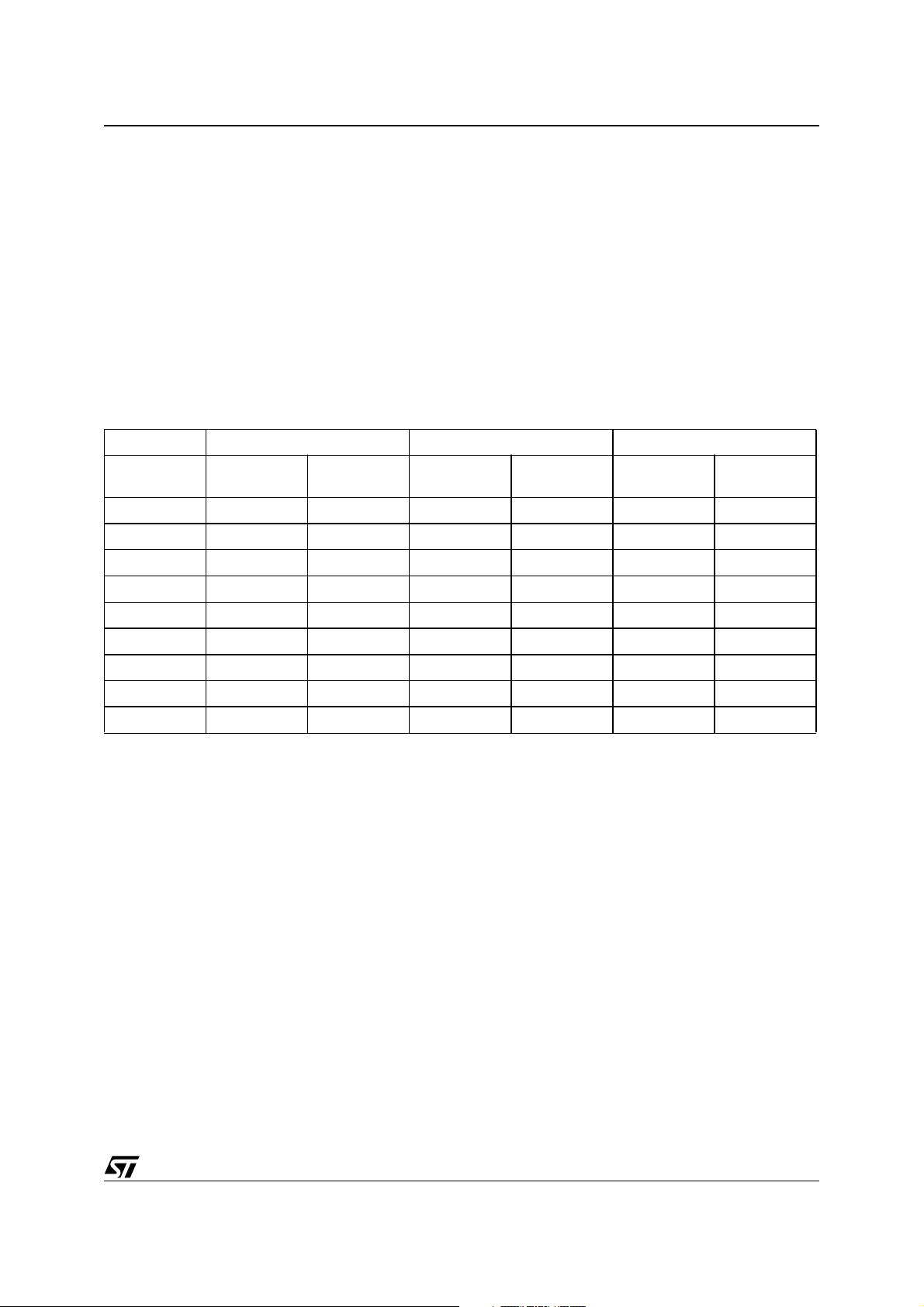
Tabl e 1. Product Range
Primary Flash
Part Number
PSD813F2 1 Mbit 256 Kbit 16 Kbit 27 24 16 yes yes
PSD813F3 1 Mbit none 16 Kbit 27 24 16 yes yes
PSD813F4 1 Mbit 256 Kbit none 27 24 16 yes yes
PSD813F5 1 Mbit none none 27 24 16 yes yes
PSD833F2 1 Mbit 256 Kbit 64 Kbit 27 24 16 yes yes
PSD834F2 2 Mbit 256 Kbit 64 Kbit 27 24 16 yes yes
PSD853F2 1 Mbit 256 Kbit 256 Kbit 27 24 16 yes yes
PSD854F2 2 Mbit 256 Kbit 256 Kbit 27 24 16 yes yes
Note: 1. All produ cts supp ort: JTAG se rial IS P, MCU para llel ISP , ISP Flash m emory , ISP CPLD, Security featur es, Power M anagem ent
2. SRAM may be backed up usin g an external battery.
(1)
Unit (PMU ), Automat i c Power-down (APD)
Memory
(8 Sectors)
Secondary
Flash Memory
4 Sectors)
SRAM
(2)
I/O Ports
Number of
Macrocells
Input Output
Serial
ISP
JTAG/
ISC Port
Turbo
Mode
6/110
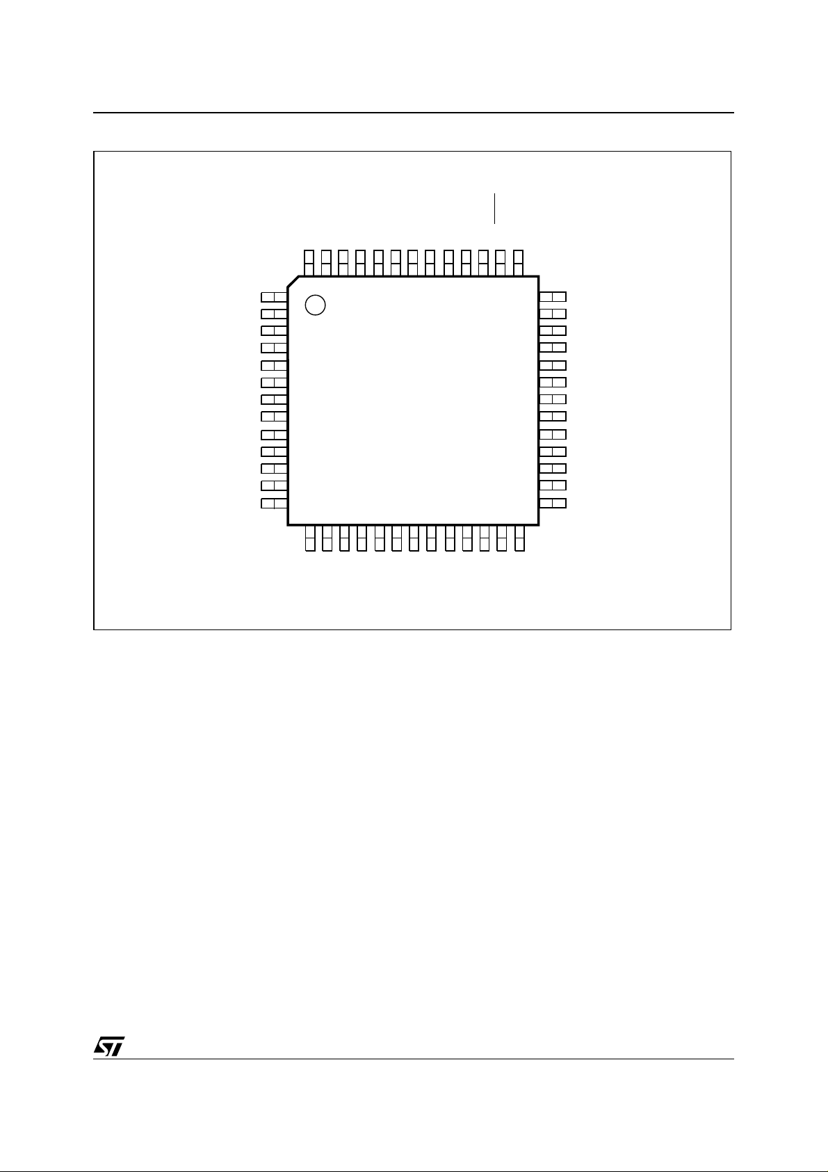
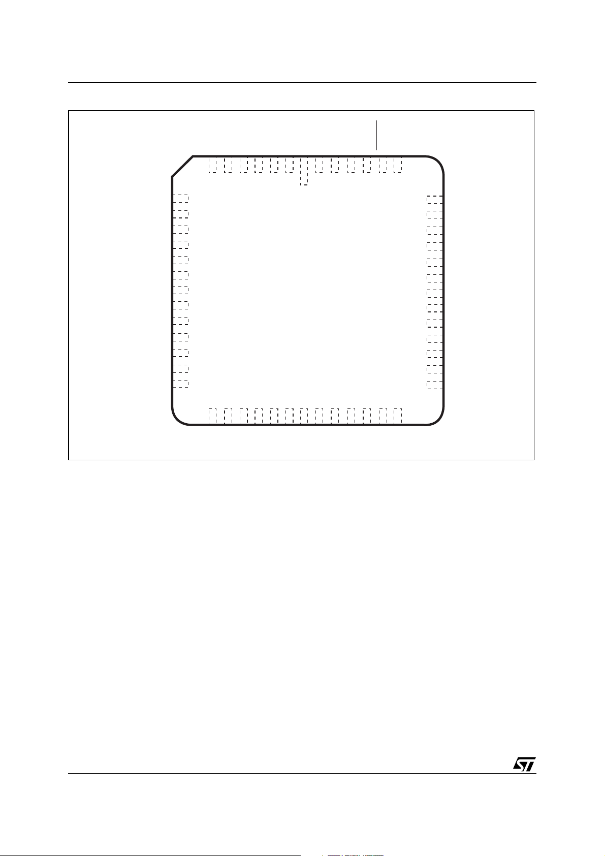
Figure 2. PQFP52 Connections
1
PD2
2
PD1
3
PD0
4
PC7
5
PC6
6
PC5
7
PC4
8
V
CC
9
GND
10
PC3
11
PC2
12
PC1
13
PC0
PSD813F2, PSD833F2, PS D834F2, PSD853F2, PSD854F2
PB0
PB1
PB2
PB3
PB4
PB5
GND
PB6
PB7
CNTL1
CNTL2
RESET
CNTLO
52515049484746454443424140
39 AD15
38 AD14
37 AD13
36 AD12
35 AD11
34 AD10
33 AD9
32 AD8
31 V
CC
30 AD7
29 AD6
28 AD5
27 AD4
14151617181920212223242526
PA7
PA6
PA5
PA4
PA3
PA2
PA1
PA0
AD0
AD1
AD2
GND
AD3
AI02858
7/110
PSD813F2, PSD833F2, PSD834F 2, PSD853F2, PSD854F2
Figure 3. PLC C5 2 C o nnections
PD2
PD1
PD0
PC7
PC6
PC5
PC4
V
CC
GND
PC3
PC2
PC1
PC0
PB0
PB1
PB2
PB3
PB4
PB5
GND
PB6
PB7
CNTL1
4
5
7
6
2
3
52
51
50
1
8
9
10
11
12
13
14
15
16
17
18
19
20
21222324252627282930313233
CNTL2
49
RESET
48
CNTL0
47
46
45
44
43
42
41
40
39
38
37
36
35
34
AD15
AD14
AD13
AD12
AD11
AD10
AD9
AD8
V
CC
AD7
AD6
AD5
AD4
PA7
PA6
PA5
PA4
PA3
GND
PA2
PA1
PA0
AD0
AD1
AD2
AD3
AI02857
8/110
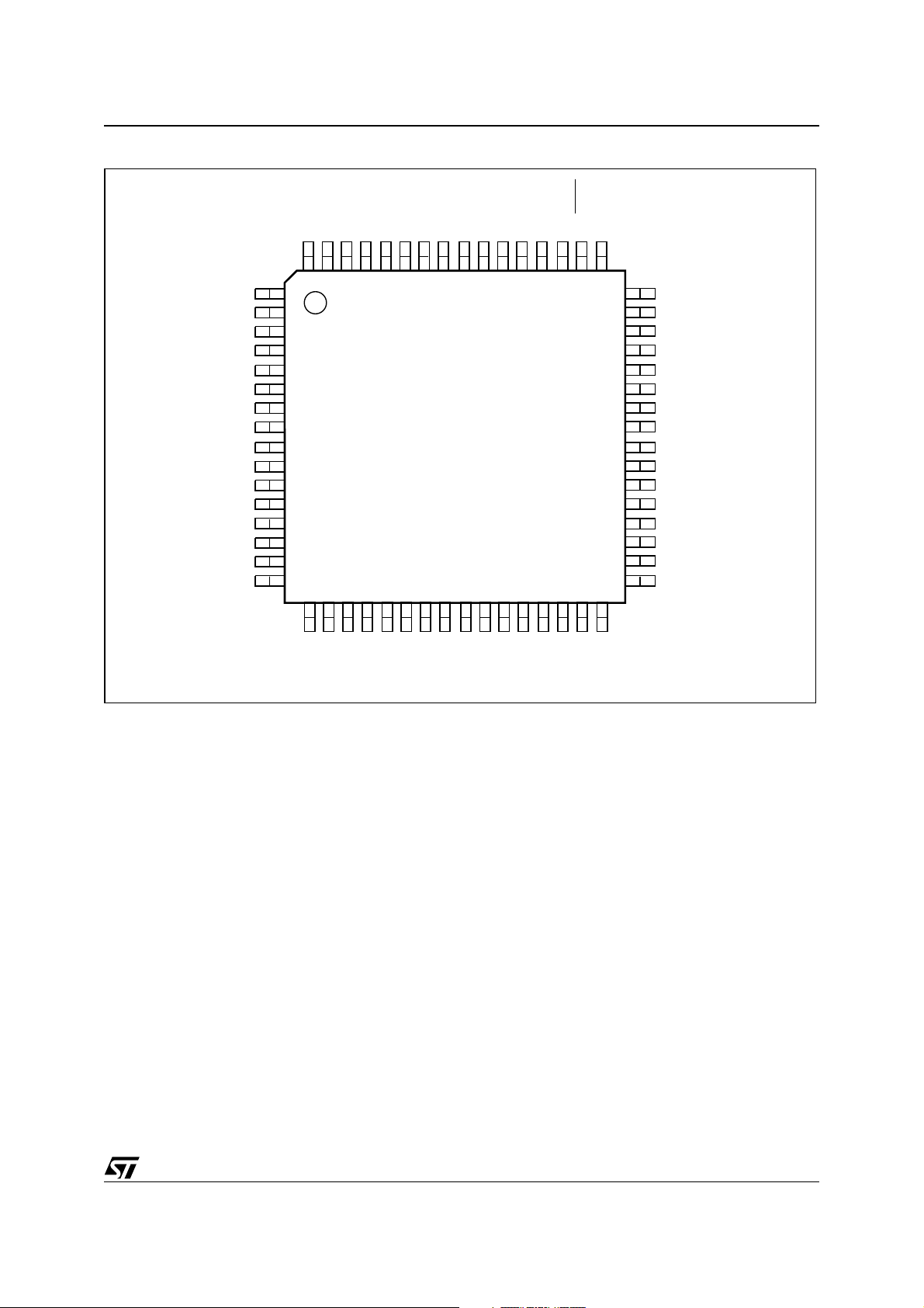
Figure 4. TQ FP 64 Connection s
PSD813F2, PSD833F2, PS D834F2, PSD853F2, PSD854F2
PD2
PD1
PD0
PC7
PC6
PC5
V
CC
V
CC
V
CC
GND
GND
PC3
PC2
PC1
PC0
NC
1
2
3
4
5
6
7
8
9
10
11
12
13
14
15
16
NCNCPB0
646362616059585756555453525150
171819202122232425262728293031
NC
NC
PA7
PB1
PA6
PB2
PA5
PB3
PA4
PB4
PA3
PB5
GND
GND
GND
GND
PA2
PB6
PA1
PB7
PA0
CNTL1
CNTL2
AD0
AD1NDAD2
RESET
NC
49
32
48 CNTL0
47 AD15
46 AD14
45 AD13
44 AD12
43 AD11
42 AD10
41 AD9
40 AD8
39 V
CC
38 V
CC
37 AD7
36 AD6
35 AD5
34 AD4
33 AD3
AI09645
9/110
PSD813F2, PSD833F2, PSD834F 2, PSD853F2, PSD854F2
PIN DES CRIPTION
Table 2. Pin Description (for the PLCC52 package - Note 1)
Pin Name Pin Type Description
This is the lower Address/Data port. Connect your MCU address or address/data bus
according to the following rules:
If your MCU has a multiplexed address/data bus where the data is multiplexed with the
lower address bits, connect AD0-AD7 to this port.
ADIO0-7 30-37 I/O
ADIO8-15 39-46 I/O
CNTL0 47 I
If your MCU does not have a multiplexed address/data bus, or you are using an 80C251
in page mode, connect A0-A7 to this port.
If you are using an 80C51XA in burst mode, connect A4/D0 through A11/D7 to this port.
ALE or AS latches the address. The PSD drives data out only if the READ signal is active
and one of the PSD functional blocks was selected. The addresses on this port are
passed to the PLDs.
This is the upper Address/Data port. Connect your MCU address or address/data bus
according to the following rules:
If your MCU has a multiplexed address/data bus where the data is multiplexed with the
lower address bits, connect A8-A15 to this port.
If your MCU does not have a multiplexed address/data bus, connect A8-A15 to this port.
If you are using an 80C251 in page mode, connect AD8-AD15 to this port.
If you are using an 80C51XA in burst mode, connect A12/D8 through A19/D15 to this
port.
ALE or AS latches the address. The PSD drives data out only if the READ signal is active
and one of the PSD functional blocks was selected. The addresses on this port are
passed to the PLDs.
The following control signals can be connected to this port, based on your MCU:
– active Low Write Strobe input.
WR
– active High READ/active Low write input.
R_W
CNTL1 50 I
CNTL2 49 I
10/110
This port is connected to the PLDs. Therefore, these signals can be used in decode and
other logic equations.
The following control signals can be connected to this port, based on your MCU:
– active Low Read Strobe input.
RD
E – E clock input.
DS – active Low Data Strobe input.
– connect PSEN to this port when it is being used as an active Low READ signal.
PSEN
For example, when the 80C251 outputs more than 16 address bits, PSEN
READ signal.
This port is connected to the PLDs. Therefore, these signals can be used in decode and
other logic equations.
This port can be used to input the PSEN
that uses this signal for code exclusively. If your MCU does not output a Program Select
Enable signal, this port can be used as a generic input. This port is connected to the
PLDs.
(Program Select Enable) signal from any MCU
is actually the

PSD813F2, PSD833F2, PS D834F2, PSD853F2, PSD854F2
Pin Name Pin Type Description
Reset 48 I
Resets I/O Ports, PLD macrocells and some of the Configuration Registers. Must be Low
at Power-up.
These pins make up Port A. These port pins are configurable and can have the following
functions:
MCU I/O – write to or read from a standard output or input port.
CPLD macrocell (McellAB0-7) outputs.
PA0
PA1
PA2
PA3
PA4
PA5
PA6
PA7
PB0
PB1
PB2
PB3
PB4
PB5
PB6
PB7
29
28
27
25
24
23
22
21
52
51
Inputs to the PLDs.
Latched address outputs (see Table 6).
I/O
Address inputs. For example, PA0-3 could be used for A0-A3 when using an 80C51XA in
burst mode.
As the data bus inputs D0-D7 for non-multiplexed address/data bus MCUs.
D0/A16-D3/A19 in M37702M2 mode.
Peripheral I/O mode.
Note: PA0-P A3 can only output CMOS signals with an option for high slew rate. However,
PA4-PA7 can be configured as CMOS or Open Drain Outputs.
These pins make up Port B. These port pins are configurable and can have the following
functions:
7
MCU I/O – write to or read from a standard output or input port.
6
5
4
3
CPLD macrocell (McellAB0-7 or McellBC0-7) outputs.
I/O
Inputs to the PLDs.
2
Latched address outputs (see Table 6).
Note: PB0-PB3 can only output CMOS signals with an option for high slew rate.
However, PB4-PB7 can be configured as CMOS or Open Drain Outputs.
PC0 pin of Port C. This port pin can be configured to have the following functions:
MCU I/O – write to or read from a standard output or input port.
PC0 20 I/O
PC1 19 I/O
CPLD macrocell (McellBC0) output.
Input to the PLDs.
2
TMS Input
for the JTAG Serial Interface.
This pin can be configured as a CMOS or Open Drain output.
PC1 pin of Port C. This port pin can be configured to have the following functions:
MCU I/O – write to or read from a standard output or input port.
CPLD macrocell (McellBC1) output.
Input to the PLDs.
2
TCK Input
for the JTAG Serial Interface.
This pin can be configured as a CMOS or Open Drain output.
11/110
PSD813F2, PSD833F2, PSD834F 2, PSD853F2, PSD854F2
Pin Name Pin Type Description
PC2 pin of Port C. This port pin can be configured to have the following functions:
MCU I/O – write to or read from a standard output or input port.
CPLD macrocell (McellBC2) output.
PC2 18 I/O
Input to the PLDs.
V
– SRAM stand-by voltage input for SRAM battery backup.
STBY
This pin can be configured as a CMOS or Open Drain output.
PC3 pin of Port C. This port pin can be configured to have the following functions:
MCU I/O – write to or read from a standard output or input port.
CPLD macrocell (McellBC3) output.
PC3 17 I/O
PC4 14 I/O
PC5 13 I/O
Input to the PLDs.
TSTAT
output2 for the JTAG Serial Interface.
Ready/Busy
output for parallel In-System Programming (ISP).
This pin can be configured as a CMOS or Open Drain output.
PC4 pin of Port C. This port pin can be configured to have the following functions:
MCU I/O – write to or read from a standard output or input port.
CPLD macrocell (McellBC4) output.
Input to the PLDs.
output2 for the JTAG Serial Interface.
TERR
Battery-on Indicator (V
). Goes High when power is being drawn from the external
BATON
battery.
This pin can be configured as a CMOS or Open Drain output.
PC5 pin of Port C. This port pin can be configured to have the following functions:
MCU I/O – write to or read from a standard output or input port.
CPLD macrocell (McellBC5) output.
Input to the PLDs.
2
TDI input
for the JTAG Serial Interface.
PC6 12 I/O
12/110
This pin can be configured as a CMOS or Open Drain output.
PC6 pin of Port C. This port pin can be configured to have the following functions:
MCU I/O – write to or read from a standard output or input port.
CPLD macrocell (McellBC6) output.
Input to the PLDs.
2
TDO output
for the JTAG Serial Interface.
This pin can be configured as a CMOS or Open Drain output.
PSD813F2, PSD833F2, PS D834F2, PSD853F2, PSD854F2
Pin Name Pin Type Description
PC7 pin of Port C. This port pin can be configured to have the following functions:
MCU I/O – write to or read from a standard output or input port.
CPLD macrocell (McellBC7) output.
PC7 11 I/O
Input to the PLDs.
DBE – active Low Data Byte Enable input from 68HC912 type MCUs.
This pin can be configured as a CMOS or Open Drain output.
PD0 pin of Port D. This port pin can be configured to have the following functions:
ALE/AS input latches address output from the MCU.
PD0 10 I/O
MCU I/O – write or read from a standard output or input port.
Input to the PLDs.
CPLD output (External Chip Select).
PD1 pin of Port D. This port pin can be configured to have the following functions:
MCU I/O – write to or read from a standard output or input port.
Input to the PLDs.
PD1 9 I/O
CPLD output (External Chip Select).
CLKIN – clock input to the CPLD macrocells, the APD Unit’s Power-down counter, and
the CPLD AND Array.
PD2 pin of Port D. This port pin can be configured to have the following functions:
MCU I/O - write to or read from a standard output or input port.
Input to the PLDs.
PD2 8 I/O
CPLD output (External Chip Select).
PSD Chip Select Input (CSI
). When Low, the MCU can access the PSD memory and I/O.
When High, the PSD memory blocks are disabled to conserve power.
V
CC
GND
Note: 1. The pin num bers in this table are for the PLCC package onl y. See the pack age informati on from Table 74., page 102 onwards, for
2. These funct i ons can be multi pl exed with ot her functi ons.
15, 38 Supply Voltage
1, 16,
26
pin numbers on other package types.
Ground pins
13/110
PSD813F2, PSD833F2, PSD834F 2, PSD853F2, PSD854F2
Figure 5. PSD Block Diagram
)
PC2
(
VSTDBY
PA0 – PA7
PB0 – PB7
PC0 – PC7
PD0 – PD2
ADDRESS/DATA/CONTROL BUS
UNIT
POWER
MANGMT
8 SECTORS
FLASH MEMORY
1 OR 2 MBIT PRIMARY
EMBEDDED
PAGE
REGISTER
256 KBIT SECONDARY
SECTOR
ALGORITHM
8
PORT
PROG.
4 SECTORS
(BOOT OR DATA)
NON-VOLATILE MEMORY
SELECTS
)
DPLD
(
PLD
FLASH DECODE
SECTOR
SELECTS
73
BACKUP SRAM
256 KBIT BATTERY
SRAM SELECT
A
PORT
RUNTIME CONTROL
AND I/O REGISTERS
PERIP I/O MODE SELECTS
CSIOP
PORT
PROG.
3 EXT CS TO PORT D
16 OUTPUT MACROCELLS
(CPLD)
FLASH ISP CPLD
73
B
PORT
PORT A ,B & C
PORT A ,B & C
24 INPUT MACROCELLS
CLKIN
C
PORT
PORT
PROG.
MACROCELL FEEDBACK OR PORT INPUT
CLKIN
PORT
PORT
PROG.
JTAG
SERIAL
& FLASH MEMORY
PLD, CONFIGURATION
D
CHANNEL
LOADER
14/110
PLD
BUS
INPUT
PROG.
CNTL0,
CNTL1,
INTRF.
MCU BUS
CNTL2
ADIO
PORT
AD0 – AD15
GLOBAL
SECURITY
CONFIG. &
CLKIN
(PD1)
AI02861E

PSD813F2, PSD833F2, PS D834F2, PSD853F2, PSD854F2
PSD ARCH ITECTURAL OVER VIEW
PSD devices contain several major functional
blocks. Figu re 5 shows the architecture of the PSD
device family. The functions of each block are described briefly in the following sections. Many of
the blocks perform multiple functions and are user
configurable.
Memory
Each of the memory blocks is briefly discussed in
the following paragraphs. A more detail ed di scussion can be found in the section entitled Memory
Blocks, page 19.
The 1 Mbit or 2 Mbit (128K x 8, or 256K x 8) Flash
memory is the primary memory of the PSD. It is divided into 8 equally-sized sectors that are individually selectable.
The optional 256 Kbit (32K x 8) secondary Flash
memory is divided into 4 equally-sized sectors.
Each sector is individually selectable.
The optional SRAM is intended for use as a
scratch-pad memory or as an extension to the
MCU SRAM. If an external battery is connected to
Voltage Stand-by (V
the event of power failure.
Each sector of mem ory can be located in a different address space as defined by the user. The access times for all memory types includes the
address latching and DPLD decoding time.
Page Regis te r
The 8-bit Page Register expands the address
range of the MCU by up to 256 times. The paged
address can be used as part of the address space
to access external memory and peripherals, or internal memory and I/O. The Page Register can
also be used to change the address mapping of
sectors of the Flash memories into different memory spaces for IAP.
PLDs
The device contains t wo PLDs, the Decode PLD
(DPLD) and the Complex PLD (CPLD), as shown
in Table 3, each op timized for a di fferent fun ction.
The functional partitioning of the PLDs reduces
power consumption, optimizes c ost/performance,
and eases design entry.
, PC2), data is retained in
STBY
The DPLD is used to decode addresses and to
generate Sector Select signals for the PSD internal memory and regis ters. The DPLD has combinatorial outputs. The CPLD has 16 Output
Macrocells (OMC) and 3 combinatorial outputs.
The PSD also has 24 Input Macrocells (IMC) that
can be configured as inputs to the PLDs. The
PLDs receive their inputs from the PLD Input Bus
and are differentiated by their output destinations,
number of product terms, and macrocells.
The PLDs consume minimal power. The speed
and power consumption of the PLD i s controlled
by the Turbo Bit in P MMR0 and other bi ts in the
PMMR2. These registers are set by the MCU at
run-time. There is a slight penalty to PLD propagation time when invoking the power m anagement
features.
I/O Po rts
The PSD has 27 individually configurable I/O pins
distributed over the four ports (Port A, B, C, and
D). Each I/O pin can be individually configured for
different functions. Ports can be configured as
standard MCU I/O ports, PLD I/O, or latched address outputs for MCUs using multiplexed address/data buses.
The JTAG pins can be enabled o n Port C for InSystem Programming (ISP).
Ports A and B can also be conf igured as a data
port for a non-multiplexed bus.
MCU Bus Interface
PSD interfaces easily with most 8-bit MCUs that
have either multiplexed or non-multiplexed address/data buses. The device is configured to respond to the MCU’s control signals, which are also
used as inputs to the PLDs. For examples, please
see the section entitled MCU Bus Interface
Examples, page 45.
Table 3. PLD I/O
Name Inputs Outputs
Decode PLD (DPLD) 73 17 42
Complex PLD (CPLD) 73 19 140
Product
Terms
15/110
PSD813F2, PSD833F2, PSD834F 2, PSD853F2, PSD854F2
JTAG Port
In-System Programming (ISP) can be pe rformed
through the JTAG signals on Port C. This serial interface allows complete programming of the entire
PSD device. A blank device can be completely
programmed. The JTAG signals (TMS, TCK,
TSTAT
, TERR, TDI, TDO) can be multiplexed with
other functions on Port C. Table 4 indicates the
JTAG pin assignments.
In-Syst em Prog r a mming ( ISP)
Using the JTAG signals on Port C, the entire PSD
device can be programmed or eras ed without the
use of the MCU. The primary Flash memory can
also be programmed in-system by the M CU executing the programming algorithms out of the secondary memory, or SRAM. The secondary
memory can be programmed the same way by executing out of the primary Flash memory. The PLD
or other PSD Configuration blocks can be programmed through the JTAG port or a de vice programmer. Table 5 indicates which programming
methods can program different functional blocks
of the PSD.
Power Management Unit (PMU)
The Power Management Unit (PMU) gives the
user control of the power consumption on selected
functional blocks based on system req uirements.
The PMU includes an Automatic Power-down
(APD) Unit that turns off device functions during
MCU inactivity. The APD Unit has a Power-down
mode tha t help s reduce po wer c onsumption.
The PSD also has some bits that are configured at
run-time by the MCU to reduce power consumption of the CPLD. The Turbo Bit in PMMR0 can be
reset to '0' and the CPLD latches its outputs and
goes to sleep until the next transition on its inputs.
Additionally, bits in PMMR2 can be set by the
MCU to block signals from entering the CP LD to
reduce power consumption. Please see t he section entitled POWER MANAGEMENT, page 62 for
more details.
Table 4. JTAG SIgnals on Port C
Port C Pins JTAG Signal
PC0 TMS
PC1 TCK
PC3 TSTAT
PC4 TERR
PC5 TDI
PC6 TDO
Table 5. Methods of Programming Different Functional Blocks of the PSD
Functional Block JTAG Programming Device Programmer IAP
Primary Flash Memory Yes Yes Yes
Secondary Flash Memory Yes Yes Yes
PLD Array (DPLD and CPLD) Yes Yes No
PSD Configuration Yes Yes No
16/110
PSD813F2, PSD833F2, PS D834F2, PSD853F2, PSD854F2
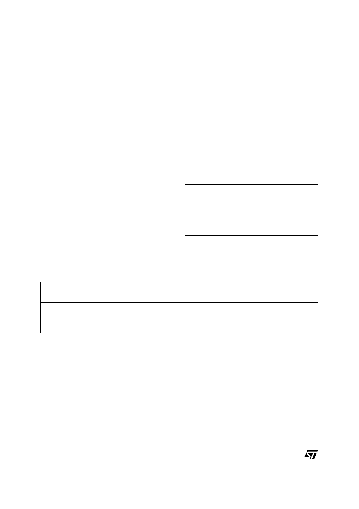
DEVELOP MEN T SYSTEM
The PSD8XXFX family is supported by PSDsoft
Express, a Windows-based software development
tool. A PSD design is quickly and easily produced
in a point and click environment. The designer
does not need to enter Hardware Description Language (HDL) equations, unless des ired, to define
PSD pin functions and memory map information.
The general design flow is shown in Figure 6. PSDsoft Express is available from our web site (the
address is given on the back page of this data
sheet) or other distribution channels.
Figure 6. PSDsoft Express Development Tool
PSDabel
PLD DESCRIPTION
MODIFY ABEL TEMPLATE FILE
OR GENERATE NEW FILE
PSDsoft Express directly supports two low cost
device programmers form ST: PSDpro and
FlashLINK (JTAG). Both of these programmers
may be purchased through your local distributor/
representative, or directly from our web site using
a credit card. The PSD is also supported by third
party device programmers. See our web site for
the current list.
PSD Configuration
CONFIGURE MCU BUS
INTERFACE AND OTHER
PSD ATTRIBUTES
LOGIC SYNTHESIS
ADDRESS TRANSLATION
AND MEMORY MAPPING
PSD Simulator
PSDsilos III
DEVICE SIMULATION
(OPTIONAL)
PSD Fitter
AND FITTING
PSD Programmer
HEX OR S-RECORD
*.OBJ FILE
PSDPro, or
FlashLINK (JTAG)
FIRMWARE
FORMAT
PSD TOOLS
GENERATE C CODE
SPECIFIC TO PSD
FUNCTIONS
USER'S CHOICE OF
MICROCONTROLLER
COMPILER/LINKER
*.OBJ AND *.SVF
FILES AVAILABLE
FOR 3rd PARTY
PROGRAMMERS
(CONVENTIONAL or
JTAG-ISC)
AI04918
17/110
PSD813F2, PSD833F2, PSD834F 2, PSD853F2, PSD854F2
PSD REGI STER DESCRIPTION AND ADDRE SS OFFSET
Table 6 shows t he offset addresses to the PSD
registers relative to the CSIOP base address. The
CSIOP space is the 256 bytes of address that is allocated by the user to the internal PSD regist ers.
Table 6. I/O Port Latched Address Output Assignments (Note1)
MCU
8051XA (8-bit) N/A Address a7-a4 Address a11-a8 N/A
80C251 (page mode) N/A N/A Address a11-a8 Address a15-a12
All other 8-bit multiplexed Address a3-a0 Address a7-a4 Address a3-a0 Address a7-a4
8-bit non-multiplexed bus N/A N/A Address a3-a0 Address a7-a4
Note: 1. See the se ct i on entitled I/O PORTS, page 51, on how to enabl e the Latched A d dress Output function.
2. N/A = Not Applicable
Port A (3:0) Port A (7:4) Port B (3:0) Port B (7:4)
Port A Port B
Table 7. Register Address Offset
Register Name Port A Port B Port C Port D
Data In 00 01 10 11 Reads Port pin as input, MCU I/O input mode
Control 02 03 Selects mode between MCU I/O or Address Out
Data Out 04 05 12 13
Direction 06 07 14 15 Configures Port pin as input or output
Drive Select 08 09 16 17
Input Macrocell 0A 0B 18 Reads Input Macrocells
Enable Out 0C 0D 1A 1B
Output Macrocells
AB
Output Macrocells
BC
Mask Macrocells AB 22 22 Blocks writing to the Output Macrocells AB
Mask Macrocells BC 23 23 Blocks writing to the Output Macrocells BC
Primary Flash
Protection
Secondary Flash
memory Protection
JTAG Enable C7 Enables JTAG Port
PMMR0 B0 Power Management Register 0
PMMR2 B4 Power Management Register 2
Page E0 Page Register
VM E2
Note: 1. Other registers that are not part of the I/O ports .
20 20
21 21
Table 7 provides brief descriptions of the registers
in CSIOP space. The following section gives a
more detailed description.
1
Other
Stores data for output to Port pins, MCU I/O
output mode
Configures Port pins as either CMOS or Open
Drain on some pins, while selecting high slew rate
on other pins.
Reads the status of the output enable to the I/O
Port driver
READ – reads output of macrocells AB
WRITE – loads macrocell flip-flops
READ – reads output of macrocells BC
WRITE – loads macrocell flip-flops
C0 Read only – Primary Flash Sector Protection
C2
Read only – PSD Security and Secondary Flash
memory Sector Protection
Places PSD memory areas in Program and/or
Data space on an individual basis.
Description
18/110
PSD813F2, PSD833F2, PS D834F2, PSD853F2, PSD854F2
DETAILED OPERATION
As shown in Figure 5., page 14 , the PS D consi s ts
of six major types of functional blocks:
■ Memory Blocks
■ PLD Blocks
■ MCU Bus Interface
■ I/O Ports
■ Power Management Unit (PMU)
■ JTAG Interface
The functions of ea ch block are described in t he
following sections. Many of the blocks perform
multiple functions, and are user configurable.
Table 8. Memory Block Siz e and Organizati on
Primary Flash Memory Secondary Flash Memory SRAM
Sector
Number
0 32K FS0 16K CSBOOT0 256K RS0
1 32K FS1 16K CSBOOT1
2 32K FS2 16K CSBOOT2
Sector Size
(Bytes)
Sector Select
Signal
Sector Size
Memory Blocks
The PSD has the following memory blocks:
– Primary Flash memory
– Optional Secondary Flash memory
– Optional SRAM
The Memory Select signals for these blocks origi-
nate from the Decode PLD (DPLD) an d are userdefined in PSDsoft Express.
(Bytes)
Sector Select
Signal
SRAM Size
(Bytes)
SRAM Select
Signal
3 32K FS3 16K CSBOOT3
4 32K FS4
5 32K FS5
6 32K FS6
7 32K FS7
Total 512K 8 Sectors 64K 4 Sectors 256K
19/110

PSD813F2, PSD833F2, PSD834F 2, PSD853F2, PSD854F2
Primary Flash Memory and Secon dary F lash
memory Description
The primary Flash memory is divided evenly into
eight equal sectors. The secondary Flash memory
is divided into four e qual sectors. Each sector of
either memory block can be sepa rately protected
from Program and Erase cycles.
Flash memory may be erased on a sector-by-sector basis. Flash sector erasure may be suspended
while data is read from other sectors of the block
and then resumed after reading.
During a Program or Erase cycle in Flash memory,
the status can be output on Ready/Busy
(PC3).
This pin is set up using PSDsoft Express Configuration.
Memory Block Select Signals
The DPLD generates the Select signals for all the
internal memory blocks (see the section entitled
PLDS, page 33). Each of the eight sectors of the
primary Flash memory has a Select signa l (FS0FS7) which can contain up to three product terms.
Each of the four sectors of the secondary Flash
memory has a Select signal (CSBOOT0CSBOOT3) which can contain up to three product
terms. Having three product terms for each Select
signal allows a given sector to be mapped in different areas of system memory. When using a MCU
with separate Program and Data space, these
flexible Select signals allow dynamic re-mapping
of sectors from one memory space to the other.
Ready/Busy
output the Ready/Busy
put on Ready/Busy
(PC3 ). This signal can be used to
status of the PSD. The out-
(PC3) is a 0 (Busy) when Flash
memory is being written to, or when Flash memory
is being erased. The output is a 1 (Ready) when
no WRITE or Erase cycle is in progress.
Memory Operation. The primary F lash memory
and secondary Flash memory are addressed
through the MCU Bus Interface. The MCU can access these memories in one of two ways:
– The MCU can execute a typical bus WRITE or
READ operation j ust as i t would if accessing a
RAM or ROM device using standard bus
cycles.
– The MCU can execute a specific instruction
that consists of several WRITE and READ
operations. This involves writing specific data
patterns to special addresses within the Flash
memory to invoke an embedded algorithm.
These instructions are summarized in Table
9., page 21.
Typically, the MCU can read Flash memory using
READ operations, just as it would read a ROM device. However, Flash memory can only be altered
using specific Erase and Program instructions. For
example, the MCU cannot write a single byte directly to Flash memory as it would write a byte to
RAM. To program a byte into F lash memory, the
MCU must execute a Program instruction, then
test the status of the Program cycle. This status
test is achieved by a RE AD operation or polling
Ready/Busy
(PC3).
Flash memory can also be read by using special
instructions to retrieve particular Flash device information (sector protect status and ID).
20/110
PSD813F2, PSD833F2, PS D834F2, PSD853F2, PSD854F2
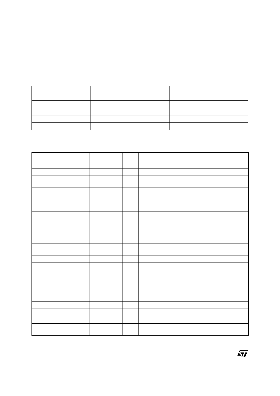
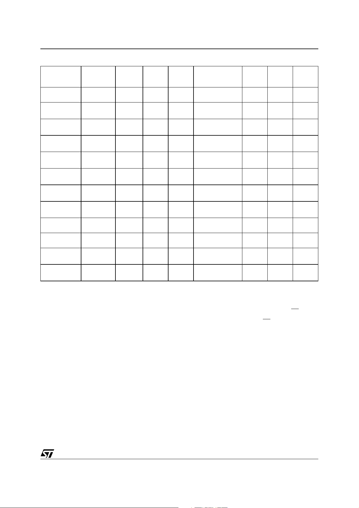
Table 9. Instructions
6,8,13
13
FS0-FS7 or
CSBOOT0-
CSBOOT3
11
12
Cycle 1 Cycle 2 Cycle 3 Cycle 4 Cycle 5 Cycle 6 Cycle 7
1
1
1
1
1
1
1
1
1
1
1
“READ”
RD @ RA
AAh@
X555h
AAh@
X555h
AAh@
X555h
AAh@
X555h
AAh@
X555h
B0h@
XXXXh
30h@
XXXXh
F0h@
XXXXh
AAh@
X555h
A0h@
XXXXh
90h@
XXXXh
55h@
XAAAh
55h@
XAAAh
55h@
XAAAh
55h@
XAAAh
55h@
XAAAh
55h@
XAAAh
PD@ PA
00h@
XXXXh
90h@
X555h
90h@
X555h
A0h@
X555h
80h@
X555h
80h@
X555h
20h@
X555h
Read identifier
(A6,A1,A0 = 0,0,1)
Read identifier
(A6,A1,A0 = 0,1,0)
PD@ PA
AAh@ X555h
AAh@ X555h
55h@
XAAAh
55h@
XAAAh
30h@
SA
10h@
X555h
, CNTL0)
Instruction
5
READ
Read Main
Flash ID
6
Read Sector
Protection
Program a
Flash Byte
Flash Sector
7,13
Erase
Flash Bulk
13
Erase
Suspend
Sector Erase
Resume
Sector Erase
6
Reset
Unlock Bypass 1
Unlock Bypass
Program
9
Unlock Bypass
10
Reset
Note: 1. All bus cycles are WRI TE bus cycles, except the ones with the “READ” labe l
2. All values ar e i n hexadecim al:
X = Don’t Care. Ad dresses of th e form XXXXh , in t h is t able, must be even addres ses
RA = Address of the memory l ocation to be read
RD = Data read from loca tion RA during the READ cy cle
PA = Address of the memory location to be programmed. Addresses are latched on the falling edge of Write Strobe (WR
PA is an even ad dress for PS D i n word program ming mod e.
PD = Data word to be programm ed at location PA. Data is latc hed on the risi ng edge of Writ e S trobe (WR
SA = Addres s of t he sector to be erased or veri fied. Th e Sect or Selec t (FS0- FS7 or C SBOOT0 -CSBO OT3) of t he sector to be
erased, or verified, must be Active (High).
3. Sector Select (FS0 to FS7 or CS BOOT0 to CSBOOT3) signals are active Hi gh, and are defi ned in PSDsof t E xpress.
4. Only address bits A11-A0 are used in instruction decoding.
5. No Unlock or i nstruction cycles are re quired when th e device is in the READ Mode
6. The Reset instruction is required to return to the READ Mode after reading the Flash ID, or after reading the Sector Protection Status, or if the Er ror Flag Bit (DQ5/DQ13) go es High.
7. Additiona l sec tors to be erased must be written at the end of the Secto r E rase instru ct i on within 80µ s.
8. The data is 00 h for an unprot ected sect or, and 01h fo r a protected s ector. In the fourth cycle, the Sector S elect is act ive, and
(A1,A0)=(1,0)
9. The Unlock Bypass instruction is required prior to the Unlock Bypass Program instruction.
10. The Unlock Bypass Reset Flash instructi on is requi red to return to readin g memory data when t he device is i n the Unloc k Bypass
mode.
11. The system may perform READ and Program cycles in non-erasing sectors, read the Flash ID or read the Sector Protection Status
when in the Suspend Sector Erase mo de. T he Suspend Sector Erase instruction is valid only during a Sec tor Erase cycl e.
12. The Resume Sector Erase instruction is valid only during the Suspend Sector Erase mode.
13. The MCU cannot inv oke the se inst ruct ion s whi le exe cutin g code fr om th e sam e Flash memory as that for whic h the i nstr uctio n is
intended. The MCU must fetch, for example, the code from the secondary Flash memory when reading the Sector Protection Status
of the prima ry Flash m em o ry.
7
@
30h
next SA
, CNTL0).
21/110

PSD813F2, PSD833F2, PSD834F 2, PSD853F2, PSD854F2
INSTRUCTIONS
An instruction consists of a sequence o f specific
operations. Each received byte is sequentially decoded by the PSD and not executed as a standard
WRITE operation. The instruction is executed
when the correct number of bytes are properly received and the time between two consecutive
bytes is shorter than the time-out period. Some instructions are structured to include READ operations after the initial WRITE operations.
The instruction must be followed exactly. Any invalid combination of instruction bytes or time-out
between two consecutive byte s while addressing
Flash memory resets the device logic into READ
Mode (Flash memory is read like a ROM device).
The PSD supports the instructions summariz ed in
Table 9., page 21:
Flash memory:
■ Erase memory by chip or sector
■ Suspend or resume sector erase
■ Program a Byte
■ Reset to READ Mode
■ Read primary Flash Identifier value
■ Read Sector Protection Status
■ Bypass (on the PSD833F2, PSD834F2,
PSD853F2 and PSD854F2)
These instructions are detailed in Table
9., page 21. For efficient decoding of the instruc-
tions, the first two bytes of an instruction are the
coded cycles and are followed by an instruction
byte or confirmation byte. The coded cy cles consist of writing the data AAh to address X555h during the first cycle and data 55h to address XAAAh
during the second cycle. Address signals A15-A12
are Don’t Care during the instruction WRITE cycles. However, the appropriate Sector Select
(FS0-FS7 or CSBOOT0-CSBOOT3) must be selected.
The primary and secondary Flash memories have
the same instruction set (except for Read Primary
Flash Identifier). The Sector Select signals determine which Flash memory is to receive and execute the instruction. The primary Flash memory is
selected if any one of Sector Select (FS0-FS7) is
High, and the secondary Flash memory is selected
if any one of Sector Select (CSBOOT0CSBOOT3) is High.
Power-up Mode
The PSD internal logic is reset upon Power-up to
the READ Mode. Sector Select (FS0-FS7 and
CSBOOT0-CSBOOT3) must be held Low, and
Write Strobe (WR
, CNTL0) High, during Power-up
for maximum security of the data contents and to
remove the possibility of a b yte being written on
the first edge of Write Strobe (WR
WRITE cycle initiation is locked when V
LKO
.
low V
READ
Under typical conditions, the MCU may read the
primary Flash memory or the secondary Flash
memory using READ operations just as it would a
ROM or RAM device. Alternately, the MCU may
use READ operations to ob tain status inform at ion
about a Program or Erase cycle that is currently in
progress. Lastly, the MCU may use instructions to
read special data from these memory blocks. The
following sections describe these READ functions.
Read Memory Contents
Primary Flash memory and secondary Flash
memory are placed in the READ Mode after Power-up, chip reset, or a Reset Flash instruction (see
Table 9., page 21). The MCU can read the memo-
ry contents of the primary Flash memory or the
secondary Flash memory by using READ operations any time the READ operation is not part of an
instruction.
Read Primary Flash Identifier
The primary Flash mem ory identifier is read with
an instruction composed of 4 operations: 3 specific
WRITE operations and a READ operation (see Ta-
ble 9., pag e 2 1). During the READ operation, ad-
dress bits A6, A1, and A0 must be '0,0,1,'
respectively, and the appropriate Sector Select
(FS0-FS7) must be High. The identifier for the
PSD813F2/3/4/5 is E4h, and for the PSD83xF2 or
PSD85xF 2 it is E7h.
Read Memory Sector Protection Status
The primary Flash memory Sector Protection Status is read with an instruction composed of 4 operations: 3 specific WRITE ope rations and a REA D
operation (see Table 9., page 21). During the
READ operation, address Bits A6, A1, and A0
must be '0,1,0,' respectively, while Sector Select
(FS0-FS7 or CSBOOT0-CSBOOT3) designates
the Flash memory sec tor whos e protection has to
be verified. The READ operation produces 01h if
the Flash memory sector is protected, or 00h if the
sector is not protected.
The sector protection status for all NVM blocks
(primary Flash memory or secondary Flash memory) can also be read by the MCU a ccessing the
Flash Protection registers in PSD I/O space. See
the section entitled Flash Memory Sector
Protect, page 28 for register definitions.
, CNT L0). An y
is be-
CC
22/110
PSD813F2, PSD833F2, PS D834F2, PSD853F2, PSD854F2
Reading the Erase/Program Status Bits
The PSD provides several status bits to be used
by the MCU to confirm the completion of an Erase
or Program cycle of Flash memory. These status
bits minimize the time that the MCU spends performing these tasks and are defined in Table 10.
The status bits can be read as many times as
needed.
Table 10. Status Bit
Functional Block
Flash Memory
Note: 1. X = Not guarant eed value , can be read either '1' or ’0.’
2. DQ7-DQ0 re present the Data Bus bit s, D7-D0.
3. FS0-FS7 and CSBOOT0- CSBOOT3 are a cti ve High.
FS0-FS7/CSBOOT0-
CSBOOT3
V
IH
DQ7 DQ6 DQ5 DQ4 DQ3 DQ2 DQ1 DQ0
Data
Polling
For Flash memory, the MCU can perform a READ
operation to obtain these status bits while an
Erase or Program instruction is being executed by
the embedded algorithm. See the section entit led
PROGRAMMING FLASH MEMORY, pag e 25 for
details.
Toggle
Flag
Error
Flag
X
Erase
Timeout
XXX
23/110

PSD813F2, PSD833F2, PSD834F 2, PSD853F2, PSD854F2
Data Polling Flag (DQ7)
When erasing or programm ing in Flash memory,
the Data Polling Flag Bit (DQ7) o utputs the complement of the bit being entered for programming/
writing on the DQ7 Bit. Once the Program instruction or the WRITE operation is completed, the true
logic value is read on the Data Polling Flag Bit
(DQ7, in a READ operation).
– Data Polling is effective after the fourth WRITE
pulse (for a Program instruction) or after the
sixth WRITE pulse (for an Erase instruction). It
must be performed at the address being
programmed or at an address within the Flash
memory sector being erased.
– During an Erase cycle, the Data Polling Flag
Bit (DQ7) outputs a ’0.’ After completion of the
cycle, the Data Polling Flag B it (DQ 7 ) o utpu ts
the last bit programmed (it is a '1' after
erasing).
– If the byte to be programmed is in a protected
Flash memory sector, the instruction is
ignored.
– If all the Flash memory sectors to be erased
are protected, the Data Polling Flag Bit (DQ7)
is reset to '0' for about 100µs, and then returns
to the previous addressed byte. No erasure is
performed.
Toggle Flag ( D Q6)
The PSD offers another way for determining when
the Flash memory Program cycle is completed.
During the internal WRITE operation and when either the FS0-FS7 or CSBOOT0-CSBOOT3 is true,
the Toggle Flag Bit (DQ6) toggles from '0' to '1' and
'1' to '0' on subsequent attemp ts to read any byte
of the memory.
When the internal cycle is complete, the toggling
stops and the data read on the Data Bus D0-D7 is
the addressed mem ory byte. The device is now
accessible for a new READ or WRITE operation.
The cycle is finished when two successive READs
yield the same output data.
– The Toggle Flag Bit (DQ6) is effective after the
fourth WRITE pulse (for a Program instruction)
or after the sixth WRITE pulse (for an Erase
instruction).
– If the byte to be programmed belongs to a
protected Flash memory sector, the
instruction is ignored.
– If all the Flash memory sectors selected for
erasure are protected, the Toggle Flag Bit
(DQ6) toggles to '0' for about 100µs and then
returns to the previous addressed byte.
Error Flag (DQ5 )
During a normal Program or Erase cycl e, the Erro r
Flag Bit (DQ5) is to ’0.’ This bit is set to '1' when
there is a failure during F lash memory Byte Program, Sector Erase, or Bulk Erase cycle.
In the case of Flash memory programming, the Error Flag Bit (DQ5) indicates the attempt to program
a Flash memory bit from the programmed state,
’0,’ to the erased state, '1,' which is not valid. The
Error Flag Bit (DQ5) may also indicate a Time-out
condition while attempting to program a byte.
In case of an error in a Flash memory Sector Erase
or Byte Progra m cycle, the Fl ash memory sector in
which the error occurred or to which the programmed byte belongs must no longer be used.
Other Flash memory sectors may still be used.
The Error Flag Bit (DQ5) is reset after a Reset
Flash instruction.
Erase Time-out Flag (DQ3)
The Erase Time-out Flag Bit (DQ3) reflects the
time-out period allowed betw een two consecut ive
Sector Erase instructions. The Erase Time-out
Flag Bit (DQ3) is reset to '0' after a Sector Erase
cycle for a time period of 100µs + 20% un less an
additional Sector Erase instruction is decoded. After this time period, or when the additional Sector
Erase instruction is decoded, the E rase Time-out
Flag Bit (DQ3) is set to '1.'
24/110
PSD813F2, PSD833F2, PS D834F2, PSD853F2, PSD854F2
PROGR AMMING FLAS H MEMORY
Flash memory must be erased prior to being programmed. A byte of Flash memory is erased to all
1s (FFh), and is programmed by setting selected
bits to ’0.’ The MCU may erase Flash memory a ll
at once or by-sector, but not byte-by-byte. However, the MCU may program Flash memory byte-bybyte.
The primary and secondary Flash memories require the MCU to send an instruction to program a
byte or to erase sectors (see Table 9., page 21).
Once the MCU issues a Flash memory Program or
Erase instruction, it must check for the status bits
for completion. The embedded algorithms that are
invoked inside the PS D s upport s everal m eans to
provide status to the MCU. Status may be checked
using any of three methods: Data Polling, Data
Toggle, or Ready/Busy
Data Polling
Polling on the Data Polling Flag Bit (DQ7) is a
method of checking whether a Program or E rase
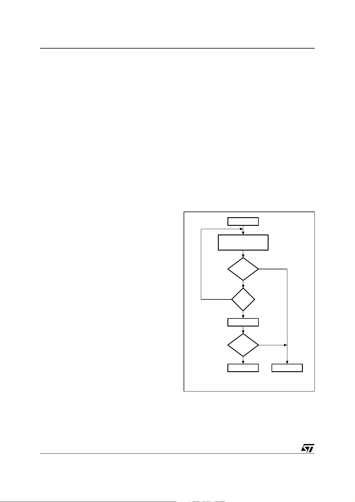
cycle is in progress or has completed. Figure 7
shows the Data Polling algorithm.
When the MCU issue s a Program i nstruction, the
embedded algorithm within th e PSD begins. The
MCU then reads the location of the byte to be programmed in Flash memory to check status. The
Data Polling Flag Bit (DQ7) of this location becomes the complement of b7 of the original data
byte to be programmed. The MCU continues to
poll this location, comparing the Data P olling Fl ag
Bit (DQ7) and monitoring the Error Flag Bit (DQ5).
When the Data Polling Flag Bit (DQ7) matches b7
of the original data, and the Error Flag Bit (DQ5)
remains ’0,’ the embedded algorithm is compl ete.
If the Error Flag Bit (DQ5) is '1,' the M CU should
test the Data Polling Flag Bit (DQ7) again since
the Data Polling Flag Bit (DQ7) may have changed
simultaneously with the Error F lag Bit (DQ5, see
Figure 7).
The Error Flag Bit (DQ5) is set if either an internal
time-out occurred while the embedded algorithm
attempted to program the byte or if the MCU a ttempted to program a '1' to a bit that was not
erased (not erased is logic '0').
It is suggested (as with all Flash memories) to read
the location again after the embedded program-
(PC3).
ming algorithm has completed, to compare the
byte that was written to the Fl ash memory with the
byte that was intended to be written.
When using the Data Polling method during an
Erase cycle, Figure 7 still app lies. However , the
Data Polling Flag Bit (DQ7) is '0' until the Erase cycle is complete. A 1 on the Error F l ag Bit (DQ5) indicates a time-out condition on the Erase cycle; a
0 indicates no error. The MCU can read any location within the sector being erased to get the Data
Polling Flag Bit (DQ7) and the Error Flag Bit
(DQ5).
PSDsoft Express generates ANSI C code functions which implement these Data Polling algorithms.
Figure 7. Data Po lli ng Flowcha rt
START
READ DQ5 & DQ7
at VALID ADDRESS
DQ7
DATA
NO
DQ5
READ DQ7
DQ7
DATA
FAIL PASS
= 1
=
=
YES
NO
YES
YES
NO
AI01369B
25/110
PSD813F2, PSD833F2, PSD834F 2, PSD853F2, PSD854F2
Data Toggle
Checking the Toggle Flag Bit (DQ6) is a method of
determining whether a Program or Erase cycle is
in progress or has completed. Figure 8 shows t he
Data Toggle algorithm.
When the MCU issue s a Program i nstruction, the
embedded algorithm within th e PSD begins. The
MCU then reads the location of the byte to be programmed in Flash memory to check status. The
Toggle Flag Bit (DQ6) of this location toggles each
time the MCU reads this location until the embedded algorithm is complete. The MCU c ontinues t o
read this location, checking the Toggle Flag Bit
(DQ6) and monitoring the Error Flag Bit (DQ5).
When the Toggle Flag Bit (DQ6) stops toggling
(two consecutive reads yield the same value), and
the Error Flag Bit (DQ5) remains ’0,’ the em bedded algorithm is complete. If the Error Flag Bit
(DQ5) is '1,' the MCU s houl d tes t th e T oggle Fl ag
Bit (DQ6) again, since the Toggle Flag Bit (DQ6)
may have changed simultaneously with the Error
Flag Bit (DQ5, see Figure 8).
The Error Flag Bit (DQ5) is set if either an internal
time-out occurred while the embedded algorithm
attempted to program the byte, or if the MCU attempted to program a '1' to a bit that was not
erased (not erased is logic '0').
It is suggested (as with all Flash memories) to read
the location again after the embedded programming algorithm has completed, to compare the
byte that was written to Flash memory with the
byte that was intended to be written.
When using the Data Toggle method after an
Erase cycle, Figure 8 still applies. the Toggle Flag
Bit (DQ6) toggles until the Erase cycle is complete.
A '1' on the Error Flag Bit (DQ5) indicates a timeout condition on the Erase cycle; a '0' indicates no
error. The MCU can read any location within the
sector being erased to get the Toggle Flag Bit
(DQ6) and the Error Flag Bit (DQ5).
PSDsoft Express generates ANSI C code functions which implement these Data Toggling a lgorithms.
Unlock Bypass (PSD833F2x, PSD834F2x,
PSD853F2x, PSD854F2x)
The Unlock Bypass instructions allow the system
to program bytes to the Flash memories faster
than using the standard Program instruction. The
Unlock Bypass mode is entered by f irst initiating
two Unlock cycles. This is followed by a third
WRITE cycle containing the Unl ock Bypas s c ode,
20h (as shown in Table 9., page 21).
The Flash memory then enters the Unlock Bypass
mode. A two-cycle Unlock Bypass Program instruction is all that is required t o program in this
mode. The first cycle in this instruction contains
the Unlock Bypass Program code, A0h. The second cycle contains the program address and data.
Additional data is programmed in the s ame manner. These instructions dispense with the initial
two Unlock cycles required in the standard Program instruction, resulting in faster total Flash
memory programming.
During the Unlock Bypass mode, only the Unlock
Bypass Program and Unlock Bypass Reset Flash
instructions are valid.
To exit th e Unlock Bypass m o de, the system mus t
issue the t wo-cycl e Unl ock Bypass Reset F lash i nstruction. The first cycle must contain the data
90h; the second cycle the data 00h. Addresses are
Don’t Care for both cycles. The Flash memory
then returns to READ Mode.
Figure 8. Dat a Toggle Flow cha rt
START
READ
DQ5 & DQ6
DQ6
=
TOGGLE
YES
NO
DQ5
= 1
YES
READ DQ6
DQ6
=
TOGGLE
YES
FAIL PASS
NO
NO
AI01370B
26/110

PSD813F2, PSD833F2, PS D834F2, PSD853F2, PSD854F2
ERASING FLASH MEMORY
Flash Bulk Erase
The Flash Bulk Erase instruction uses six WRITE
operations followed by a READ operat ion of the
status register, as described in Tab le 9., page 21.
If any byte of the Bulk Era se instruction is wrong,
the Bulk Erase instruction aborts and the device is
reset to the Read Flash memory status.
During a Bulk Erase, the memory status may be
checked by reading the Error Flag Bit (DQ5), the
Toggle Flag Bit (DQ6), and the Data Polling Fl ag
Bit (DQ7), as detailed in the section entitled PRO-
GRAMMING FLASH MEMORY , page 25. The Er-
ror Flag Bit (DQ5) returns a '1' if there has been an
Erase Failure (maximum number of Erase cycles
have been executed).
It is not necessary to program the memory with
00h because the PSD automatically does this before erasing to 0FFh.
During execution of the Bulk Erase instruction, the
Flash memory does not accept any instructions.
Flash Sector Erase
The Sector Erase instruction uses six WRITE operations, as described in Table 9., page 21. Addi-
tional Flash Sector Erase codes and Flash
memory sector addresses can be written subsequently to erase other Flash memory sectors in
parallel, without further coded cycles, if the additional bytes are transmitted in a sho rter time than
the time-out period of about 100µs. The in put of a
new Sector Erase code restarts the time-out period.
The status of the internal timer can be m onitored
through the level of the Erase Time-out Flag Bit
(DQ3). If the Erase Time-out Flag B it (DQ3) is ’0,’
the Sector Erase instruction has been received
and the time-out period is counting. If the Erase
Time-out Flag Bit (DQ3) is '1,' the time-out period
has expired and the PSD is busy erasing the Flash
memory sector(s). Before and during Erase timeout, any instruction other than Suspend Sector
Erase and Resume Sector Erase instructions
abort the cycle that is currently in progress, and reset the device to READ Mode. It is not necessary
to program the Flash mem ory sector with 00h as
the PSD does this automatically before erasing
(byte = FFh).
During a Sector Erase, the memory status may be
checked by reading the Error Flag Bit (DQ5), the
Toggle Flag Bit (DQ6), and the Data Polling Fl ag
Bit (DQ7), as detailed in the section entitled PRO-
GRAMMING FLASH MEMORY, page 25.
During execution of the Erase cycle, the Flash
memory accepts only Reset and Suspend Sector
Erase instructions. Erasure of one Flash memory
sector may be suspended, in order to read data
from another Flash memory se ctor, and then resumed.
Suspend Sector Erase
When a Sector Erase cycle is in progress, the Suspend Sector Erase instruction can be used to suspend the cycle by writing 0B0h to any address
when an appropriate Sector Select (FS0-FS7 or
CSBOOT0-CSBOOT3) is High. (See Table
9., page 21). This allows reading of data from an-
other Flash memory sector after the Erase cycle
has been suspended. Suspend Sector Erase is
accepted only during an Erase cycle and defaults
to READ Mode. A Suspend S ector Erase instruction executed during an Erase time-o ut period, in
addition to suspending the Erase cycle, terminates
the time out pe rio d.
The Toggle Flag Bit (DQ6) stops toggling when the
PSD internal logic is suspended. The status of this
bit must be monitored at an address within the
Flash memory sector being erased. The Toggle
Flag Bit (DQ6) stops toggling between 0.1µ s and
15µs after the Suspend Sector Erase instruction
has been executed. The PSD is then automatically
set to READ Mode.
If an Suspend Sector Erase instruction was executed, the following rules apply:
– Attempting to read from a Flash memory
sector that was being erased outputs invalid
data.
– Reading from a Flash sector that was not
being erased is valid.
– The Flash memory cannot be programmed,
and only responds to Resume Sector Erase
and Reset Flash instructions (READ is an
operation and is allowed).
– If a Reset Flash instruction is received, data in
the Flash memory sector that was being
erased is invalid.
Resume Sector Erase
If a Suspend Sector E rase instruction was previously executed, the erase cycle may be resumed
with this instruction. The Resume Sector Erase instruction consists of writing 030h to any address
while an appropriate Sector Select (FS0-FS7 or
CSBOOT0-CSBOOT3) is High. (See Table
9., page 21.)
27/110
PSD813F2, PSD833F2, PSD834F 2, PSD853F2, PSD854F2
SPECIFIC FEATURES
Flash Memory Sector Protect
Each primary and secondary Flash memory sector
can be separately protected a gainst P rogram and
Erase cycle s. Sector Pr ote c ti o n p r o vi d es a ddi tional data security because it disables all Program or
Erase cycles. This mode ca n be activated through
the JTAG Port or a Device Programmer.
Sector protection can be selected for ea ch sector
using the PSDsoft Express Configuration program. This automatically protects selected sectors
when the device is programmed through the JTAG
Port or a Device Programmer. Flash memory sectors can be unprotecte d to allow updating of t heir
contents using the JTAG Port or a Device Programmer. The MCU can read (but cannot change)
the sector protection bits.
Any attempt to program or erase a protected Flash
memory sector is ignored by the device. The Verify
operation results in a READ of the protected data.
This allows a guarantee of the retention of the Protection status.
The sector protection status ca n be read by the
MCU through the Flash memory protection and
PSD/EE protection registers (in the CSIOP block).
See Tables 11 and 12.
Reset Flash
The Reset Flash instruction consists of one
WRITE cycle (see Table 9., page21). It can also
be optionally preceded by the standard two
WRITE decoding cycles (writing AAh to 555h and
55h to AAAh). It must be executed after:
– Reading the Flash Protection Status or Flash
ID
– An Error condition has occurred (and the
device has set the Error Flag Bit (DQ5) to '1')
during a Flash memory Program or Erase
cycle.
On the PSD813F2/3/4/5, the Reset Fla sh instruction puts the Flash memory back into normal
READ Mode. It may take the Flash memory up to
a few milliseconds to complete the Reset cycle.
The Reset Flash instruction is ignored when it is issued during a Program or Bulk Erase cycle of the
Flash memory. The Reset Flash instruction aborts
any on-going Sector Erase cycle, and returns the
Flash memory to the normal READ Mode within a
few millis econds.
On the PSD83xF2 or PSD85xF2, the Reset Flash
instruction puts the Flash m emory back into normal READ Mode. If an Error condition has occurred (and the device has set the Error Flag Bit
(DQ5) to '1') the Flash memory is put back into normal READ Mode within 25µs of the Reset Flash instruction having been issued. The Reset Flash
instruction is ignored when it is issued during a
Program or Bulk Erase cycle of the Flash memory.
The Reset Flash instruction a borts any on-going
Sector Erase cycle, and returns the Flash memory
to the normal READ Mode within 25µs.
Reset (RESET
PSD85xF2)
A pulse on Reset (RESET
in progress, and resets the Flash memory to the
READ Mode. When the reset occurs during a Program or Erase cycle, the Flash memory takes up
to 25 µs to return to the READ Mode. It is recommended that the Reset (RESET
Power On Reset, as described on RESET TIMING
AND DEVICE STATUS AT RESET, page 67) be
at least 25µs so that the F lash memory is always
ready for the MCU to fetch the bootstrap instructions after the Reset cycle is complete .
) Signal (on the PSD83xF2 and
) aborts any cycle that is
) pulse (except for
Table 11. Sector Protection/Security Bit Definition – Flash Protection Register
Bit 7Bit 6Bit 5Bit 4Bit 3Bit 2Bit 1Bit 0
Sec7_Prot Sec6_Prot Sec5_Prot Sec4_Prot Sec3_Prot Sec2_Prot Sec1_Prot Sec0_Prot
Note: 1. Bit Definitions:
Sec<i>_Prot 1 = Primary Flash memory or secondary Flash memory Sector <i> is write protected.
Sec<i>_Prot 0 = Primary F lash memory or secondary Fla sh memory Sec to r <i > i s no t write protec ted.
Table 12. Sector Protection/Security Bit Definition – PSD/EE Protection Register
Bit 7Bit 6Bit 5Bit 4Bit 3Bit 2Bit 1Bit 0
Security_Bit not used not used not used Sec3_Prot Sec2_Prot Sec1_Prot Sec0_Prot
Note: 1. Bit Definitions:
28/110
Sec<i>_Prot 1 = Secondary Flash memory Sector <i> is write protected.
Sec<i>_Prot 0 = Secondary Fl ash memo ry Sect or <i> is not write protected.
Security_Bit 0 = Security Bit in device has not been set.
1 = Security Bi t in device has be en set.

PSD813F2, PSD833F2, PS D834F2, PSD853F2, PSD854F2
SRAM
The SRAM is enab led when SRAM Select (RS0)
from the DPLD is High. SRAM Select (RS0) can
contain up to two prod uct terms, allowing flexib le
memory mapping.
The SRAM can be backed up usin g an external
battery. The external battery should be connected
to Voltage Stand-by (V
external battery connected to the PSD , the contents of the SRAM are reta ined in the event of a
power loss. The contents of the SRAM are retained so long as the battery voltage remains at
2 V or greater. If the supply voltage falls below the
battery voltage, an internal power switch-over to
the battery occurs.
, PC2). If you have an
STBY
PC4 can be configured as an output that indicates
when power is being drawn from the ext ernal ba ttery. Battery-on Indicator (VBATON, PC4) is High
with the supply voltage falls below the battery voltage and the battery on Voltage Stand-by (V
STBY
PC2) is supplying power to the internal SRAM.
SRAM Select (RS0), Voltage Stand-by (V
STBY
PC2) and Battery-on Indicator (VBATON, PC4)
are all configured using PSDsoft Express Configuration.
,
,
29/110

PSD813F2, PSD833F2, PSD834F 2, PSD853F2, PSD854F2
SECTOR SELECT AND SRAM SE LECT
Sector Select (FS0-FS7, CSBOOT0-CSBOOT3)
and SRAM Select (RS0) are all outputs of the
DPLD. They are setup by writing equations for
them in PSDabel. The f ollowing rules apply to the
equations for these signals:
1. Primary Flash memory and secondary Flash
memory Sector Select signals must not be
larger than the physical sector size.
2. Any p rimary Flas h memory sector must not be
mapped in the same memory space as
another Flash memory sector.
3. A secondary Flash memory sector must not be
mapped in the same memory space as
another secondary Flash memory sector.
4. SRAM, I/O, and Peripheral I/O spaces must
not overlap.
5. A secondary Flash memory sector may
overlap a prim ary Flash m emory sector. In
case of overlap, priority is given to the
secondary Flash memory sector.
6. SRAM, I/O, and Peripheral I/O spaces may
overlap any other memory sector. Priority is
given to the SRAM, I/O, or Peripheral I/O.
Example
FS0 is valid when the address is in the range of
8000h to BFFFh, CSBOOT0 is valid from 8000h to
9FFFh, and RS0 is valid from 8000h to 87FFh.
Any address in the range of RS0 always accesses
the SRAM. Any address in the range of CSBOOT0
greater than 87FFh (and less than 9FF Fh) automatically addresses secondary Flash memory
segment 0. Any address greater than 9FFFh ac cesses the primary Flash memory segment 0. You
can see that half of the primary Flash memory segment 0 and one-fourth of secondary Flash memory
segment 0 cannot be acces sed in this example.
Also note that an equation that defined FS1 to anywhere in the range of 8000h to BFFFh wo uld not
be valid.
Figure 9 show s the priority lev els for all me mory
components. Any component on a higher level can
overlap and has priority over any component on a
lower level. Components on the same level must
not overlap. Level one has the highest priority and
level 3 has the lowest.
Memory Se le c t Co nf i gur a tio n f or MCUs with
Separate Program and Data Spaces
The 8031 and compatible family of MCUs, which
includes the 80C51, 80C151, 80C251, and
80C51XA, have separate address spaces for Program memory (selected using Program Select Enable (PSEN
using Read Strobe (RD
, CNTL2)) and Data memory (selected
, CNTL1)). Any of the
memories within the PSD can reside in either
space or both spaces.
This is controlled through manipulation of the VM
register that resides in the CSIOP space.
The VM register is set using PSDsoft Express to
have an initial value. It can subsequently be
changed by the MCU so that memory mapping
can be changed on-the-fly.
For example, you may wish to have SRAM and primary Flash memory in the Data space at Boot-up,
and secondary Flash memory in the Program
space at Boot-up, and later s wap the primary and
secondary Flash memories. This is easily done
with the VM register by using PSDsoft Express
Configuration to configure it for Boot-up and having the MCU change it when desired. Table
13., page 31 descr ibes the VM Register.
Figure 9. Priority Level of Memory and I/O
Components
Highest Priority
Lowest Priority
Conf i gurat i on Modes for MCUs with Sepa rate
Program and Data Spaces
Separate Space Modes. Program space is sep-
arated from Data space. For example, Program
Select Enable (PSEN
the program code from the primary Flash memory,
while Read Strobe (RD
data from the secondary Flash memory, SRAM
and I/O Port blocks. This configuration requires
the VM register to be set to 0Ch (see Figure
10., page 31).
Combined Space Modes. The Program and
Data spaces are combined into one memory
space that allows the primary Flash memory, secondary Flash memory, and SRAM to be accessed
by either Program Select Enable (PSEN
or Read Strobe (RD
configure the primary Flash mem ory in Combi ned
space, Bits b2 and b4 of the VM register are set to
'1' (see Figure 11., page 31).
Level 1
SRAM, I/O, or
Peripheral I/O
Level 2
Secondary
Non-Volatile Memory
Level 3
Primary Flash Memory
, CNTL2) is used to a ccess
, CNTL1) is used to access
, CNTL1). For example, to
AI02867D
, CNTL2)
30/110
 Loading...