

查询PSD4235G2V供应商
Flash In-System Programmable (ISP) Peripherals
FEATURES SUMMARY
PSD provides an integrated solution to 16-bit MCU
based applications that includes configurable
memories, PLD logic and I/O:
■ Dual Bank Flash Memories
– 4 Mbit of Primary Flash Memory (8 uniform
sectors, 32K x 16)
– 256 Kbit Secondary Flash Memory with 4
sectors
– Concurrent operation: read from one memory
while erasing and writing the other
■ 64 Kbit SRAM (Battery Backed)
■ PLD with macrocells
– Over 3000 Gates of PLD: CPLD and DPLD
– CPLD with 16 Output Macrocells (OMCs) and
24 Input Macrocells (IMCs)
– DPLD – user defined in ternal chip select de-
coding
■ Seven l/O Ports with 52 I/O pins
– 52 individually conf igurable I / O port p ins that
can be used for the following functions:
– MCU I/Os
–PLD I/Os
– Latched MCU address output
– Special function l/Os
– l/O ports may be configured as open-drain
outputs
■ In-System Programming (ISP) with JTAG
– Built-in JTAG compliant serial port allows full-
chip In-System Programmability
– Efficient manufacturing allow easy product
testing and programming
– Use low cost FlashLINK cable with PC
■ Page Register
– Internal page register that can be used to ex-
pand the microcontroller address space by a
factor of 256
PSD4235G2V
For 16-bit MCUs (3.3V Supply)
PRELIMINARY DATA
■ Programmable power management
■ High Endurance:
– 100,000 Erase/Write Cycles of Flash Memory
– 1,000 EraseWrite Cycles of PLD
– 15 Year Data Retention
■ Single Supply Voltage
– 3.3V ±10%
■ Memory Speed
– 90ns Flash memory and SRAM access time
Figure 1. Packages
TQFP80 (U)
December 2001
This is preliminary information on a new product now in development or undergoing evaluation. Details are subject to change without notice.
1/89

PSD4235G2V
TABLE OF CONTENTS
Summary Description . . . . . . . . . . . . . . . . . . . . . . . . . . . . . . . . . . . . . . . . . . . . . . . . . . . . . . . . . . . . . . 5
In-System Programming (ISP) via JTAG. . . . . . . . . . . . . . . . . . . . . . . . . . . . . . . . . . . . . . . . . . . . . . 5
In-Application Programming (IAP). . . . . . . . . . . . . . . . . . . . . . . . . . . . . . . . . . . . . . . . . . . . . . . . . . . 6
PSDsoft Express . . . . . . . . . . . . . . . . . . . . . . . . . . . . . . . . . . . . . . . . . . . . . . . . . . . . . . . . . . . . . . . . 7
PSD Architectural Overview . . . . . . . . . . . . . . . . . . . . . . . . . . . . . . . . . . . . . . . . . . . . . . . . . . . . . . . . . 8
Memory . . . . . . . . . . . . . . . . . . . . . . . . . . . . . . . . . . . . . . . . . . . . . . . . . . . . . . . . . . . . . . . . . . . . . . . 8
PLDs . . . . . . . . . . . . . . . . . . . . . . . . . . . . . . . . . . . . . . . . . . . . . . . . . . . . . . . . . . . . . . . . . . . . . . . . . 8
I/O Ports . . . . . . . . . . . . . . . . . . . . . . . . . . . . . . . . . . . . . . . . . . . . . . . . . . . . . . . . . . . . . . . . . . . . . . 8
MCU Bus Interface . . . . . . . . . . . . . . . . . . . . . . . . . . . . . . . . . . . . . . . . . . . . . . . . . . . . . . . . . . . . . . 8
ISP via JTAG Port . . . . . . . . . . . . . . . . . . . . . . . . . . . . . . . . . . . . . . . . . . . . . . . . . . . . . . . . . . . . . . . 8
In-System Programming (ISP). . . . . . . . . . . . . . . . . . . . . . . . . . . . . . . . . . . . . . . . . . . . . . . . . . . . . . 8
In-Application Programming (IAP). . . . . . . . . . . . . . . . . . . . . . . . . . . . . . . . . . . . . . . . . . . . . . . . . . . 8
Page Register . . . . . . . . . . . . . . . . . . . . . . . . . . . . . . . . . . . . . . . . . . . . . . . . . . . . . . . . . . . . . . . . . . 9
Power Management Unit (PMU) . . . . . . . . . . . . . . . . . . . . . . . . . . . . . . . . . . . . . . . . . . . . . . . . . . . . 9
Development System. . . . . . . . . . . . . . . . . . . . . . . . . . . . . . . . . . . . . . . . . . . . . . . . . . . . . . . . . . . . . . 10
Pin Description. . . . . . . . . . . . . . . . . . . . . . . . . . . . . . . . . . . . . . . . . . . . . . . . . . . . . . . . . . . . . . . . . . . 11
PSD Register Description and Address Offsets . . . . . . . . . . . . . . . . . . . . . . . . . . . . . . . . . . . . . . . . 14
Register Bit Definition. . . . . . . . . . . . . . . . . . . . . . . . . . . . . . . . . . . . . . . . . . . . . . . . . . . . . . . . . . . . . 15
Detailed Operation. . . . . . . . . . . . . . . . . . . . . . . . . . . . . . . . . . . . . . . . . . . . . . . . . . . . . . . . . . . . . . . . 20
Memory Blocks . . . . . . . . . . . . . . . . . . . . . . . . . . . . . . . . . . . . . . . . . . . . . . . . . . . . . . . . . . . . . . . . 20
Instructions . . . . . . . . . . . . . . . . . . . . . . . . . . . . . . . . . . . . . . . . . . . . . . . . . . . . . . . . . . . . . . . . . . . 23
Reading Flash Memory . . . . . . . . . . . . . . . . . . . . . . . . . . . . . . . . . . . . . . . . . . . . . . . . . . . . . . . . . . 23
Programming Flash Memory. . . . . . . . . . . . . . . . . . . . . . . . . . . . . . . . . . . . . . . . . . . . . . . . . . . . . . 25
Erasing Flash Memory. . . . . . . . . . . . . . . . . . . . . . . . . . . . . . . . . . . . . . . . . . . . . . . . . . . . . . . . . . . 26
Flash Memory Sector Protect . . . . . . . . . . . . . . . . . . . . . . . . . . . . . . . . . . . . . . . . . . . . . . . . . . . . . 27
Reset. . . . . . . . . . . . . . . . . . . . . . . . . . . . . . . . . . . . . . . . . . . . . . . . . . . . . . . . . . . . . . . . . . . . . . . . 28
SRAM . . . . . . . . . . . . . . . . . . . . . . . . . . . . . . . . . . . . . . . . . . . . . . . . . . . . . . . . . . . . . . . . . . . . . . . 28
Memory Select Signals . . . . . . . . . . . . . . . . . . . . . . . . . . . . . . . . . . . . . . . . . . . . . . . . . . . . . . . . . . 28
Page Register . . . . . . . . . . . . . . . . . . . . . . . . . . . . . . . . . . . . . . . . . . . . . . . . . . . . . . . . . . . . . . . . . 30
2/89

PSD4235G2V
Memory ID Registers. . . . . . . . . . . . . . . . . . . . . . . . . . . . . . . . . . . . . . . . . . . . . . . . . . . . . . . . . . . . 31
PLDs . . . . . . . . . . . . . . . . . . . . . . . . . . . . . . . . . . . . . . . . . . . . . . . . . . . . . . . . . . . . . . . . . . . . . . . . 31
Decode PLD (DPLD). . . . . . . . . . . . . . . . . . . . . . . . . . . . . . . . . . . . . . . . . . . . . . . . . . . . . . . . . . . . . . . 33
Complex PLD (CPLD) . . . . . . . . . . . . . . . . . . . . . . . . . . . . . . . . . . . . . . . . . . . . . . . . . . . . . . . . . . . . . 34
MCU Bus Interface. . . . . . . . . . . . . . . . . . . . . . . . . . . . . . . . . . . . . . . . . . . . . . . . . . . . . . . . . . . . . . . . 40
I/O Ports . . . . . . . . . . . . . . . . . . . . . . . . . . . . . . . . . . . . . . . . . . . . . . . . . . . . . . . . . . . . . . . . . . . . . . . . 50
Port Operating Modes . . . . . . . . . . . . . . . . . . . . . . . . . . . . . . . . . . . . . . . . . . . . . . . . . . . . . . . . . . . 51
Ports A, B and C – Functionality and Structure. . . . . . . . . . . . . . . . . . . . . . . . . . . . . . . . . . . . . . . . 56
Port D – Functionality and Structure . . . . . . . . . . . . . . . . . . . . . . . . . . . . . . . . . . . . . . . . . . . . . . . . 57
Port E – Functionality and Structure . . . . . . . . . . . . . . . . . . . . . . . . . . . . . . . . . . . . . . . . . . . . . . . . 57
Port F – Functionality and Structure . . . . . . . . . . . . . . . . . . . . . . . . . . . . . . . . . . . . . . . . . . . . . . . . 58
Port G – Functionality and Structure. . . . . . . . . . . . . . . . . . . . . . . . . . . . . . . . . . . . . . . . . . . . . . . . 58
Power Management . . . . . . . . . . . . . . . . . . . . . . . . . . . . . . . . . . . . . . . . . . . . . . . . . . . . . . . . . . . . . . . 59
PLD Power Management . . . . . . . . . . . . . . . . . . . . . . . . . . . . . . . . . . . . . . . . . . . . . . . . . . . . . . . . 61
PSD Chip Select Input (CSI, PD2) . . . . . . . . . . . . . . . . . . . . . . . . . . . . . . . . . . . . . . . . . . . . . . . . . 61
Power On Reset, Warm Reset and Power-down . . . . . . . . . . . . . . . . . . . . . . . . . . . . . . . . . . . . . . 62
Programming In-Circuit using the JTAG Serial Interface. . . . . . . . . . . . . . . . . . . . . . . . . . . . . . . . . 63
Initial Delivery State . . . . . . . . . . . . . . . . . . . . . . . . . . . . . . . . . . . . . . . . . . . . . . . . . . . . . . . . . . . . . . . 64
AC/DC Parameters. . . . . . . . . . . . . . . . . . . . . . . . . . . . . . . . . . . . . . . . . . . . . . . . . . . . . . . . . . . . . . . . 65
Table. Absolute Maximum Ratings . . . . . . . . . . . . . . . . . . . . . . . . . . . . . . . . . . . . . . . . . . . . . . . . .68
Table. Operating Conditions . . . . . . . . . . . . . . . . . . . . . . . . . . . . . . . . . . . . . . . . . . . . . . . . . . . . . . 69
Table. DC Characteristics . . . . . . . . . . . . . . . . . . . . . . . . . . . . . . . . . . . . . . . . . . . . . . . . . . . . . . . . 71
Table. CPLD Combinatorial Timing. . . . . . . . . . . . . . . . . . . . . . . . . . . . . . . . . . . . . . . . . . . . . . . . .72
Table. CPLD Macrocell Synchronous Clock Mode Timing . . . . . . . . . . . . . . . . . . . . . . . . . . . . . . . 72
Table. CPLD Macrocell Asynchronous Clock Mode Timing . . . . . . . . . . . . . . . . . . . . . . . . . . . . . . 73
Table. Input Macrocell Timing . . . . . . . . . . . . . . . . . . . . . . . . . . . . . . . . . . . . . . . . . . . . . . . . . . . . . 75
Table. Read Timing . . . . . . . . . . . . . . . . . . . . . . . . . . . . . . . . . . . . . . . . . . . . . . . . . . . . . . . . . . . . . 76
Table. Write Timing . . . . . . . . . . . . . . . . . . . . . . . . . . . . . . . . . . . . . . . . . . . . . . . . . . . . . . . . . . . . . 78
Table. Port F Peripheral Data Mode Read Timing . . . . . . . . . . . . . . . . . . . . . . . . . . . . . . . . . . . . . 80
Table. Port F Peripheral Data Mode Write Timing. . . . . . . . . . . . . . . . . . . . . . . . . . . . . . . . . . . . . . 81
Table. Reset (Reset) Timing . . . . . . . . . . . . . . . . . . . . . . . . . . . . . . . . . . . . . . . . . . . . . . . . . . . . . . 82
Table. VSTBYON Timing . . . . . . . . . . . . . . . . . . . . . . . . . . . . . . . . . . . . . . . . . . . . . . . . . . . . . . . . . 82
Table. Program, Write and Erase Times. . . . . . . . . . . . . . . . . . . . . . . . . . . . . . . . . . . . . . . . . . . . .82
Table. ISC Timing . . . . . . . . . . . . . . . . . . . . . . . . . . . . . . . . . . . . . . . . . . . . . . . . . . . . . . . . . . . . . .83
Table. Power-down Timing . . . . . . . . . . . . . . . . . . . . . . . . . . . . . . . . . . . . . . . . . . . . . . . . . . . . . . . 84
3/89

PSD4235G2V
Package Mechanical . . . . . . . . . . . . . . . . . . . . . . . . . . . . . . . . . . . . . . . . . . . . . . . . . . . . . . . . . . . . . . 85
Table. TQFP80 - 80 lead Plastic Quad Flatpack. . . . . . . . . . . . . . . . . . . . . . . . . . . . . . . . . . . . . . . 85
Table. Pin Assignments – TQFP80. . . . . . . . . . . . . . . . . . . . . . . . . . . . . . . . . . . . . . . . . . . . . . . . . 86
Table. Ordering Information Scheme . . . . . . . . . . . . . . . . . . . . . . . . . . . . . . . . . . . . . . . . . . . . . . .87
4/89
SUMMARY DESCRIPTION
The PSD family of memory systems for microcontrollers (MCUs) brings In-System-Programmability
(ISP) to Flash memory and programmable logic.
The result is a simple and flexible solution for embedded designs. PSD dev ices combine many of
the peripheral functions found in MCU based applications.
PSD devices integrate an optimized Macrocell logic architecture. The Macrocell was creat ed to address the unique requirements of embedded
system designs. It allows direct connection between the system address/data bus, and the internal PSD registers, to simplify communication
between the MCU and other supporting devices.
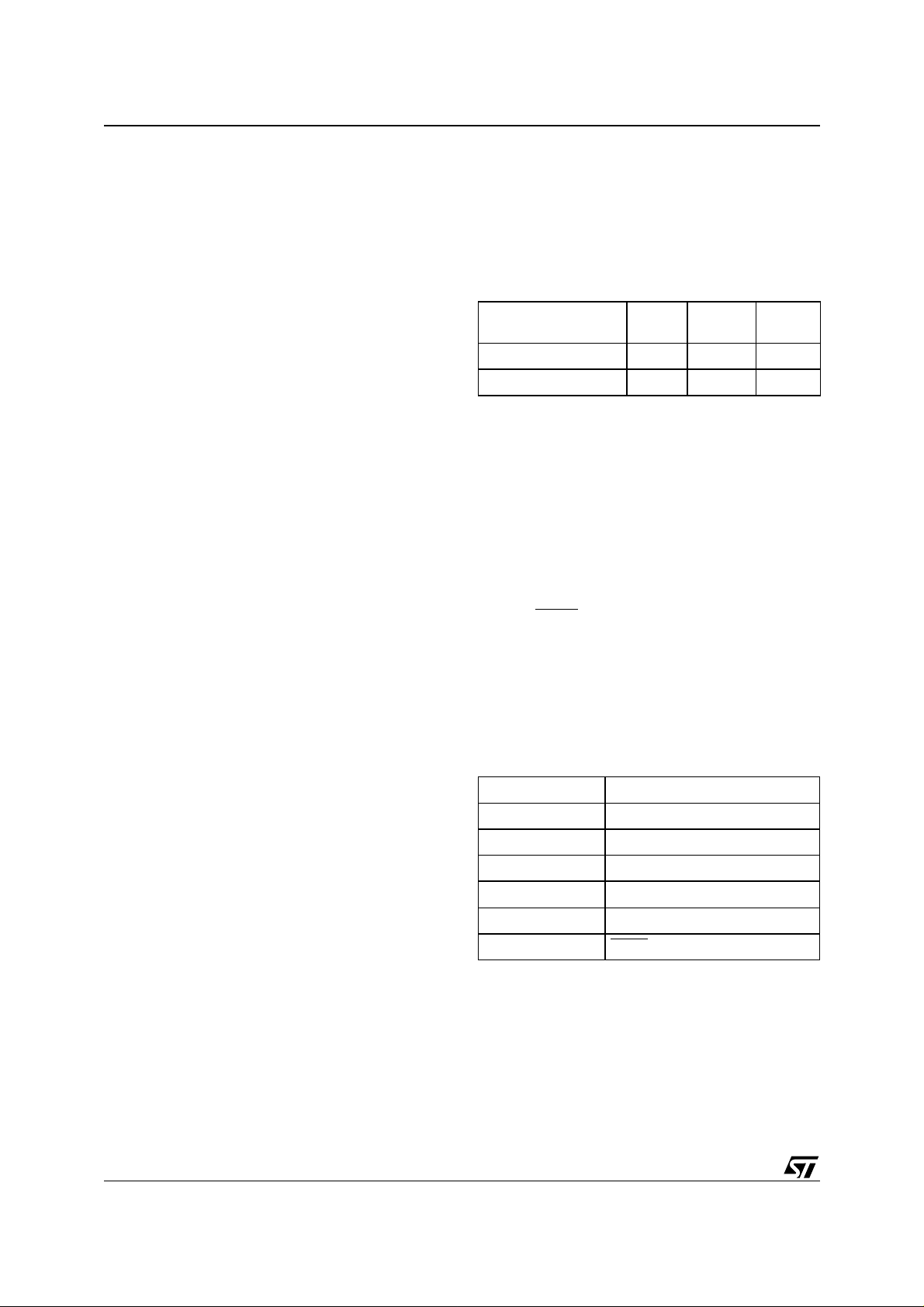
Table 1. Pin Names
PA0-PA7 Port-A
PB0-PB7 Port-B
PC0-PC7 Port-C
PD0-PD3 Port-D
PE0-PE7 Port-E
PF0-PF7 Port-F
PG0-PG7 Port-G
AD0-AD15 Address/Data
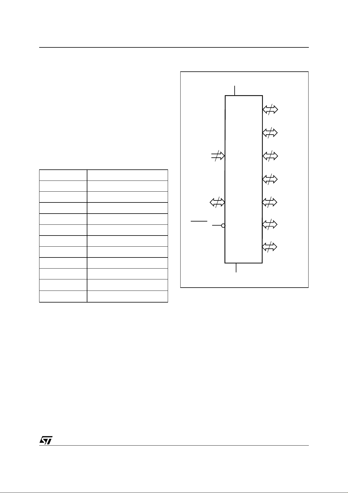
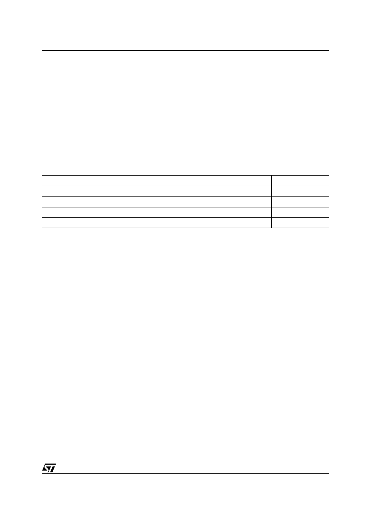
Figure 2. Logic Diagram
V
CC
3
CNTL0-
CNTL2
PSD4xxxGx
16
AD0-AD15
RESET
PSD4235G2V
8
PA0-PA7
8
PB0-PB7
8
PC0-PC7
4
PD0-PD3
8
PE0-PE7
8
PF0-PF7
8
PG0-PG7
CNTL0-CNTL2 Control
RESET Reset
V
CC
V
SS
Supply Voltage
Ground
The PSD family offers two methods to program the
PSD Flash me mory while the PSD is soldered t o
the circuit board: In-System Programming (ISP)
via JTAG, and In-Application Programming (IAP).
In-System Programming (ISP) via JTAG
An IEEE 1149.1 compliant JTAG In-System Programming (ISP) interface is inclu ded on the P SD
enabling the entire device (Flash m emo ries, PLD,
configuration) to be rapidly programmed while soldered to the circuit board. This requires no MCU
participation, which means the PSD can be programmed anytime, even when completely blank.
The innovative JTAG interface to Flash memories
is an industry first, solving key problems faced by
designers and manufacturing houses, such as:
V
SS
AI04916
First time programming. How do I get firmware
into the Flash memory the very first time? JTAG is
the answer. Program the blank PSD with no MCU
involvement.
Inventory build-up of pre-programme d devices. How do I maintain an ac curate count of pre-
programmed Flash memory and PLD devices
based on customer demand? How many and what
version? JTAG is the answer. Build your hardware
with blank PSDs soldered directly to the board and
then custom program just before they are shipped
to the customer. No more labels on chips, and no
more wasted inventory.
Expensive sockets. How do I eliminate the need
for expensive and unreliable sockets? JTAG is the
answer. Solder the PSD directly to the circuit
board. Program first time and subsequent times
with JTAG. No need to handle devices and b end
the fragile leads.
5/89
PSD4235G2V
Figure 3. TQ FP Connection s
PD1
PD0
80797877767574737271706968676665646362
PE7
PE6
PE5
PE4
PE3
PE2
PE1
PE0
GND
VCCPB7
PB6
PB5
PB4
PB3
PB2
PB1
PB0
61
PD2
PD3
AD0
AD1
AD2
AD3
AD4
GND
V
CC
AD5
AD6
AD7
AD8
AD9
AD10
AD11
AD12
AD13
AD14
AD15
1
2
3
4
5
6
7
8
9
10
11
12
13
14
15
16
17
18
19
20
21222324252627282930313233343536373839
CC
PF0
PF1
PF2
PF3
PF4
PF5
PF6
PG0
PG1
PG2
PG3
PG4
PG5
PG6
PG7
V
GND
PF7
RESET
40
CNTL2
60 CNTL1
59 CNTL0
58 PA7
57 PA6
56 PA5
55 PA4
54 PA3
53 PA2
52 PA1
51 PA0
50 GND
49 GND
48 PC7
47 PC6
46 PC5
45 PC4
44 PC3
43 PC2
42 PC1
41 PC0
AI04943
In-Appl i c at io n P rog ra m m i ng (IA P)
Two independent Flash memory arrays are included so that the MCU can execute code from one
while erasing and programming the o the r. Robu st
product firmware updates in the filed a re possible
over any communication channel (CAN, Ethernet,
UART, J1850, etc) using this unique architecture.
Designers are relieved of these problems:
Simultaneous rea d and write to Flash memory. How can the MCU program the same memory
from which it executing code? It canno t. The P S D
allows the MCU to operate the two Flash me mory
blocks concurrently, reading code from one while
erasing and programming the other during IAP.
Complex memory mapping. How can I map
these two memories efficiently? A program mable
6/89
Decode PLD (DPLD) is embedded in the PSD.
The concurrent PSD memories can be mapped
anywhere in MCU address space, segment by
segment with extermely hi gh address resolution.
As an option, the secondary Flash memory can be
swapped out of the system memory map when
IAP is complete. A built-in page register breaks the
MCU add re ss limit.
Separate Program and Data space. How can I
write to Flash memory while it res ide s in Program
space during field firmware updates? My
80C51XA will not allow it. The PSD provides
means to reclassify Flash m em ory as Data space
during IAP, then back to Program space when
complete.
PSD4235G2V
PSDsoft Express
PSDsoft Express, a software development tool
from ST, guides you through the design process
step-by-step making it possible to complete an
embedded MCU design capable of ISP/IAP in just
hours. Select your MCU and PSDsoft Express
takes you through the remainder of the design with
point and click entry, covering PSD selection, pin
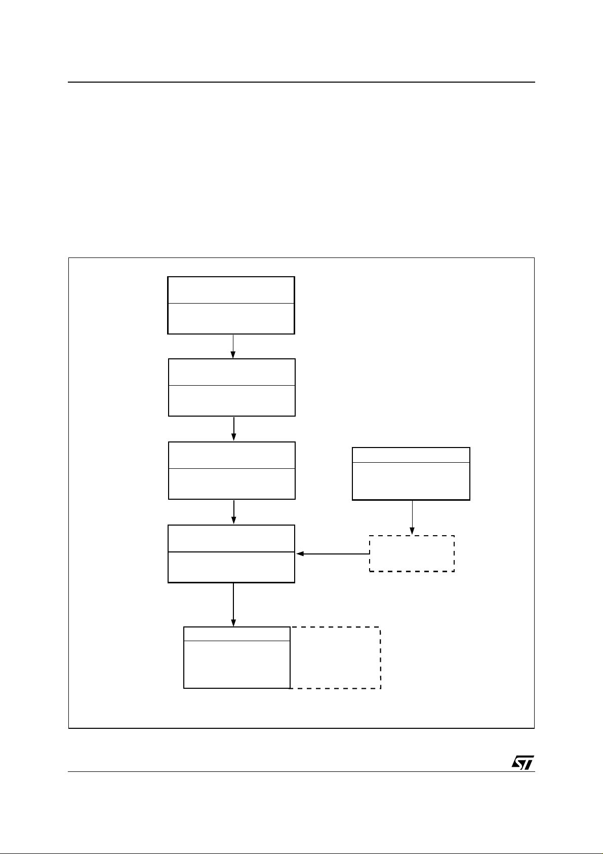
Figure 4. PSD Block Diagram
)
PE6
(
VSTDBY
PA0 – PA7
UNIT
POWER
MANGMT
4 MBIT PRIMARY
FLASH MEMORY
16 SECTORS
4 SECTORS
FLASH MEMORY
(BOOT OR DATA)
256 KBIT SECONDARY
PORT
PROG.
BACKUP SRAM
64 KBIT BATTERY
definitions, programmable logic inputs and outpus,
MCU memory map definition, ANSI-C code generation for your MCU, and merging your MCU firmware with the PSD design. When complete, two
different device programmers are supported directly from PSDsoft Express: FlashLINK (JTAG)
and PSDpro.
A
PORT
PB0 – PB7
PORT
PROG.
B
PORT
PC0 – PC7
PORT
PROG.
PORT
C
PORT F
PD0 – PD3
PORT
PROG.
D
PORT
PROG.
JTAG
SERIAL
PE0 – PE7
PORT
CHANNEL
E
PORT
PORT A & B
8 EXT CS TO PORT C or F
16 OUTPUT MACROCELLS
(CPLD)
FLASH ISP CPLD
82
F
PORT
PORT
PROG.
PF0 – PF7
ADDRESS/DATA/CONTROL BUS
PLD
BUS
INPUT
EMBEDDED
PAGE
REGISTER
ALGORITHM
8
SECTOR
SELECTS
)
(
FLASH DECODE
PROG.
MCU BUS
CNTL0,
CNTL1,
CNTL2
DPLD
PLD
INTRF.
SECTOR
SELECTS
82
RUNTIME CONTROL
AND I/O REGISTERS
SRAM SELECT
PERIP I/O MODE SELECTS
CSIOP
ADIO
PORT
AD0 – AD15
Note: Additio nal address li nes can be brou ght in to the devi ce via Port A, B, C, D or F.
PORT A ,B & C
24 INPUT MACROCELLS
MACROCELL FEEDBACK OR PORT INPUT
CLKIN
G
PORT
PORT
PROG.
PG0 – PG7
CLKIN
LOADER
& FLASH MEMORY
PLD, CONFIGURATION
GLOBAL
SECURITY
CONFIG. &
CLKIN
AI04990
7/89
PSD4235G2V
PSD ARCHITECTURAL OVERVIEW
PSD devices contain several major functional
blocks. Figur e 4 shows the architect ure of the PSD
device family. The functions of each block are described briefly in the following sections. Many of
the blocks perform multiple functions and are user
configurable.
Memory
Each of the memory blocks is briefly discussed in
the following paragraphs. A more detailed discus-
sion can be found in the section entitled “Memory
Blocks“ on page 20.
The 4 Mbit primary Flash memory is the main
memory of the P SD. It is divided into 8 eq uallysized sectors that are individually selectable.
The 256 K bit s econdary Flash mem ory i s divided
into 4 equally-sized sectors. Each sector is individually selectable.
The 64 Kbit SRAM is intended for use as a
scratch-pad memory or as an extension to the
MCU SRAM. If an external battery is connected to
the PSD’s Voltage Stand-by (VSTBY, PE6) signal,
data is retained in the event of power failure.
Each memory block can be located in a different
address space as defined by the user. The access
times for all memory types includes the address
latching and DPLD decoding time.
PLDs
The device contains two PLD blocks, the Decode
PLD (DPLD) and the Complex PLD (CPLD), as
shown in Table 2, each optimized for a different
function. The functional partitioning of the PLDs
reduces power consumption, optim izes cost/performance, and eases design entry.
The DPLD is used to decode addresses and to
generate Sector Select signals for the PSD internal memory and regis ters. Th e DPLD has combinatorial outputs, while the CPLD can implement
more general user-defined logic functions. The
CPLD has 16 Output Macrocells (OMC) and 8
combinatorial outputs. The PSD also has 24 Input
Macrocells (IMC) that can be configured as inputs
to the PLDs. The PLDs receive their inputs from
the PLD Input Bus and are di fferentiated by their
output destinations, number of product terms, and
Macrocells.
The PLDs consume minimal power. The speed
and power consumption of the PLD i s controlled
by the Turbo bit in PMMR0 and other bits in
PMMR2. These registers are set by the MCU at
run-time. There is a slight penalty to PLD propagation time when not in the Turbo mode.
I/O Po r t s
The PSD has 52 I/O pins divided among seven
ports (Port A, B, C, D, E, F and G). Each I/O pin
can be individually configured for different func-
tions. Ports can be configured as standard MCU I/
O ports, PLD I/O, or latched address outputs for
MCUs using multiplexed address/data buses
The JTAG pins can be e nabled on Port E for InSystem Programming (ISP).
Table 2. PLD I/O
Name Inputs Outputs
Decode PLD (DPLD) 82 17 43
Complex PLD (CPLD) 82 24 150
Product
Terms
MCU Bus Interface
The PSD easily interfaces easily with most 16-bit
MCUs, either with multiplexed or non-multiplexed
address/data buses. The device is configured to
respond to the MCU’s control pins, which are also
used as inputs to the PLDs.
ISP via JTAG Port
In-System Programming (ISP) can be pe rformed
through the JTAG signals on Port E. This serial interface allows complete programming of the entire
PSD device. A blank device can be completely
programmed. The JTAG signals (TMS, TCK,
TSTAT, TERR
, TDI, TDO) can be multiplexed with
other functions on Port E. Table 3 indicates the
JTAG pin assignments.
In-System Progr a mming ( ISP)
Using the JTAG signals on Port E, the entire PSD
device (memory, logic, configuration) can be programmed or erased without the use of the MCU.
Table 3. JTAG SIgnals on Port E
Port E Pins JTAG Signal
PE0 TMS
PE1 TCK
PE2 TDI
PE3 TDO
PE4 TSTAT
PE5 TERR
In-Application Programming (IAP)
The primary Flash memory can also be programmed, or re-programmed, in-system by the
MCU executing the programming algorithms out of
the secondary Flash memory, or SRAM. The secondary Flash memory can be programmed the
same way by executing out of the primary Flash
memory. Table 4 indicates which programming
methods can program different functional blo cks
of the PSD.
8/89
PSD4235G2V
Page Re gi st er
The 8-bit Page Register expands the address
range of the MCU by up to 256 times. The paged
address can be used as part of the address space
to access external memory and peripherals, or internal memory and I/O. The Page Register can
also be used to change the address mapping of
the Flash memory blocks into different memory
spaces for IAP.
Power Management Unit (PMU)
The Power Management Unit (PMU) gives the
user control of the power consumption on selected
functional blocks based on system req uirements.
The PMU includes an Automatic Power-down
(APD) Unit that turns off device functions during
MCU inactivity. The APD Unit has a Power-down
mode tha t helps redu ce pow er co nsumption.
The PSD also has some bits that are configured at
run-time by the MCU to reduce power consumption of the CPLD. The Turbo bit in PMMR0 can be
reset to 0 and the CPLD l atches its outputs and
goes to Stand-by mode until the next transition on
its inputs.
Additionally, bits in PMMR2 can be set by the
MCU to block signals from entering the CPLD t o
reduce power consumption. See th e section enti-
tled “Power Management” on page 59 for more details.
Table 4. Methods of Programming Different Functional Blocks of the PSD
Functional Block JTAG-ISP Device Programmer IAP
Primary Flash Memory Yes Yes Yes
Secondary Flash memory Yes Yes Yes
PLD Array (DPLD and CPLD) Yes Yes No
PSD Configuration Yes Yes No
9/89
PSD4235G2V
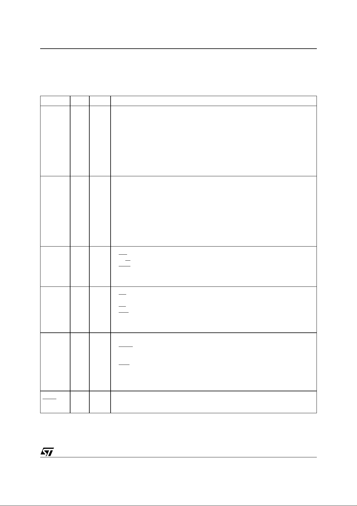
DEVELOPMENT SYST EM
The PSD family is supported by PSDsoft Express,
a Windows-based software development tool
(Windows-95, Windows-98, Windows-2000, Windows-NT). A PSD design is quickly and easily produced in a point and click environment. The
designer does not need to enter Hardware Description Language (HDL) equations, unless desired, to define PSD pin functions and memory
map information. The general design flow is
shown in Figure 5. PSDsof t Express is available
from our web site (the address is given on the back
Figure 5. PSDsoft Express Developmen t Tool
Choose MCU and PSD
Automatically configures MCU
bus interface and other
PSD attributes
Define PSD Pin and
Node Functions
Point and click definition of
PSD pin functions, internal nodes,
and MCU system memory map
page of this data sheet) or other distribution channels.
PSDsoft Express directly supports two low cost
device programmers form ST: PSDpro and
FlashLINK (JTAG). Both of these programmers
may be purchased through your local distributor/
representative, or directly from our web site using
a credit card. The PSD is also supported by t hid
party device programmers. See our web site for
the current list.
Define General Purpose
Logic in CPLD
Point and click definition of combinatorial and registered logic in CPLD.
Access HDL is available if needed
Merge MCU Firmware
with PSD Configuration
A composite object file is created
containing MCU firmware and
PSD configuration
*.OBJ FILE
PSD Programmer
PSDPro, or
FlashLINK (JTAG)
MCU FIRMWARE
HEX OR S-RECORD
FORMAT
*.OBJ FILE
AVAILABLE
FOR 3rd PARTY
PROGRAMMERS
(CONVENTIONAL or
JTAG-ISC)
C Code Generation
GENERATE C CODE
SPECIFIC TO PSD
FUNCTIONS
USER'S CHOICE OF
MICROCONTROLLER
COMPILER/LINKER
AI04919
10/89
PIN DESCRIPTION
Table 5 describes the signal names and signal
functions of the PSD. Those that have multiple
names or functions are defined using PSDsoft Express.
Table 5. Pin Description (for the TQFP package)
Pin Name Pin Type Description
This is the lower Address/Data port. Connect your MCU address or address/data bus
according to the following rules:
1. If your MCU has a multiplexed address/data bus where the data is multiplexed with
the lower address bits, connect AD0-AD7 to this port.
ADIO0ADIO7
ADIO8ADIO15
CNTL0 59 I
CNTL1 60 I
CNTL2 40 I
Reset
3-7
10-12
13-20 I/O
39 I
I/O
2. If your MCU does not have a multiplexed address/data bus, connect A0-A7 to this
port.
3. If you are using an 80C51XA in burst mode, connect A4/D0 through A11/D7 to this
port.
ALE or AS latches the address. The PSD drives data out only if the read signal is active
and one of the PSD functional blocks has been selected. The addresses on this port
are passed to the PLDs.
This is the upper Address/Data port. Connect your MCU address or address/data bus
according to the following rules:
1. If your MCU has a multiplexed address/data bus where the data is multiplexed with
the upper address bits, connect A8-A15 to this port.
2. If your MCU does not have a multiplexed address/data bus, connect A8-A15 to this
port.
3. If you are using an 80C51XA in burst mode, connect A12/D8 through A19/D15 to this
port.
ALE or AS latches the address. The PSD drives data out only if the read signal is active
and one of the PSD functional blocks has been selected. The addresses on this port
are passed to the PLDs.
The following control signals can be connected to this pin, based on your MCU:
– active Low, Write Strobe input.
1. WR
– active High, read/active Low write input.
2. R_W
3. WRL
– active Low, Write to Low-byte.
This pin is connected to the PLDs. Therefore, these signals can be used in decode and
other logic equations.
The following control signals can be connected to this pin, based on your MCU:
1. RD
– active Low, Read Strobe input.
2. E – E clock input.
– active Low, Data Strobe input.
3. DS
– active Low, Strobe for low data byte.
4. LDS
This pin is connected to the PLDs. Therefore, these signals can be used in decode and
other logic equations.
Read or other Control input pin, with multiple configurations. Depending on the MCU
interface selected, this pin can be:
1. PSEN
mode).
2. BHE – High-byte enable, 16-bit data bus.
3. UDS
4. SIZ0 – Byte enable input.
5. LSTRB – Low Strobe input.
This pin is also connected to the PLDs.
Active Low input. Resets I/O Ports, PLD Macrocells and some of the Configuration
Registers and JTAG registers. Must be Low at Power-up. Reset also aborts any Flash
memory Program or Erase cycle that is currently in progress.
– Program Select Enable, active Low in code fetch bus cycle (80C51XA
– active Low, Strobe for high data byte, 16-bit data bus mode.
PSD4235G2V
11/89
PSD4235G2V
Pin Name Pin Type Description
These pins make up Port A. These port pins are configurable and can have the
following functions:
1. MCU I/O – standard output or input port.
2. CPLD Macrocell (McellA0-McellA7) outputs.
3. Latched, transparent or registered PLD inputs (can also be PLD input for address
A16 and above).
These pins make up Port B. These port pins are configurable and can have the
following functions:
1. MCU I/O – standard output or input port.
2. CPLD Macrocell (McellB0-McellB7) outputs.
3. Latched, transparent or registered PLD inputs (can also be PLD input for address
A16 and above).
PA0-PA7 51-58
PB0-PB7 61-68
I/O
CMOS
or
Open
Drain
I/O
CMOS
or
Open
Drain
PC0-PC7 41-48
PD0 79
PD1 80
PD2 1
PD3 2
PE0 71
PE1 72
PE2 73
I/O
CMOS
or
Slew
Rate
I/O
CMOS
or
Open
Drain
I/O
CMOS
or
Open
Drain
I/O
CMOS
or
Open
Drain
I/O
CMOS
or
Open
Drain
I/O
CMOS
or
Open
Drain
I/O
CMOS
or
Open
Drain
I/O
CMOS
or
Open
Drain
These pins make up Port C. These port pins are configurable and can have the
following functions:
1. MCU I/O – standard output or input port.
2. External Chip Select (ECS0-ECS7) outputs.
3. Latched, transparent or registered PLD inputs (can also be PLD input for address
A16 and above).
PD0 pin of Port D. This port pin can be configured to have the following functions:
1. ALE/AS input – latches address on ADIO0-ADIO15.
input – latches address on ADIO0-ADIO15 on the rising edge.
2. AS
3. MCU I/O – standard output or input port.
4. Transparent PLD input (can also be PLD input for address A16 and above).
PD1 pin of Port D. This port pin can be configured to have the following functions:
1. MCU I/O – standard output or input port.
2. Transparent PLD input (can also be PLD input for address A16 and above).
3. CLKIN – clock input to the CPLD Macrocells, the APD Unit’s Power-down counter,
and the CPLD AND Array.
PD2 pin of Port D. This port pin can be configured to have the following functions:
1. MCU I/O – standard output or input port.
2. Transparent PLD input (can also be PLD input for address A16 and above).
3. PSD Chip Select Input (CSI
I/O. When High, the PSD memory blocks are disabled to conserve power. The falling
edge of this signal can be used to get the device out of Power-down mode.
PD3 pin of Port D. This port pin can be configured to have the following functions:
1. MCU I/O – standard output or input port.
2. Transparent PLD input (can also be PLD input for address A16 and above).
3. WRH
PE0 pin of Port E. This port pin can be configured to have the following functions:
1. MCU I/O – standard output or input port.
2. Latched address output.
3. TMS Input for the JTAG Serial Interface.
PE1 pin of Port E. This port pin can be configured to have the following functions:
1. MCU I/O – standard output or input port.
2. Latched address output.
3. TCK Input for the JTAG Serial Interface.
PE2 pin of Port E. This port pin can be configured to have the following functions:
1. MCU I/O – standard output or input port.
2. Latched address output.
3. TDI input for the JTAG Serial Interface.
– for 16-bit data bus, write to high byte, active low.
). When Low, the MCU can access the PSD memory and
12/89
Pin Name Pin Type Description
PE3 74
PE4 75
PE5 76
PE6 77
PE7 78
PF0-PF7 31-38
PG0-PG7 21-28
V
CC
9, 29,
69
I/O
CMOS
or
Open
Drain
I/O
CMOS
or
Open
Drain
I/O
CMOS
or
Open
Drain
I/O
CMOS
or
Open
Drain
I/O
CMOS
or
Open
Drain
I/O
CMOS
or
Open
Drain
I/O
CMOS
or
Open
Drain
PE3 pin of Port E. This port pin can be configured to have the following functions:
1. MCU I/O – standard output or input port.
2. Latched address output.
3. TDO output for the JTAG Serial Interface.
PE4 pin of Port E. This port pin can be configured to have the following functions:
1. MCU I/O – standard output or input port.
2. Latched address output.
3. TSTAT output for the JTAG Serial Interface.
4. Ready/Busy
PE5 pin of Port E. This port pin can be configured to have the following functions:
1. MCU I/O – standard output or input port.
2. Latched address output.
3. TERR
PE6 pin of Port E. This port pin can be configured to have the following functions:
1. MCU I/O – standard output or input port.
2. Latched address output.
3. VSTBY – SRAM stand-by voltage input for SRAM battery backup.
PE7 pin of Port E. This port pin can be configured to have the following functions:
1. MCU I/O – standard output or input port.
2. Latched address output.
3. Battery-on Indicator (VBATON). Goes High when power is being drawn from the
external battery.
These pins make up Port F. These port pins are configurable and can have the following
functions:
1. MCU I/O – standard output or input port.
2. External Chip Select (ECS0-ECS7) outputs, or inputs to CPLD.
3. Latched address outputs.
4. Address A1-A3 inputs in 80C51XA mode (PF0 is grounded)
5. Data bus port (D0-D7) in a non-multiplexed bus configuration.
6. Peripheral I/O mode.
7. MCU reset mode.
These pins make up Port G. These port pins are configurable and can have the
following functions:
1. MCU I/O – standard output or input port.
2. Latched address outputs.
3. Data bus port (D8-D15) in a non-multiplexed bus configuration.
4. MCU reset mode.
Supply Voltage
output for parallel In-System Programming (ISP).
active Low output for the JTAG Serial Interface.
PSD4235G2V
GND
8, 30,
49,
50, 70
Ground pins
13/89
PSD4235G2V
PSD REGISTER DESCRIPTION AND ADDRESS OFFSETS
Table 6 shows the offset addresses to the PSD
registers relative to the CSIOP base address. The
CSIOP space is the 256 bytes of address that is allocated by the user to the internal PS D registers.
Table 6. Register Address Offset
Register Name
Data In 00 01 10 11 30 40 41 Reads Port pin as input, MCU I/O input mode
Control 32 42 43
Data Out 04 05 14 15 34 44 45
Direction 06 07 16 17 36 46 47 Configures Port pin as input or output
Drive Select 08 09 18 19 38 48 49
Input Macrocell 0A 0B 1A Reads Input Macrocells
Enable Out 0C 0D 1C 4C
Output
Macrocells A
Output
Macrocells B
Mask
Macrocells A
Mask
Macrocells B
Flash Memory
Protection
Flash Boot
Protection
JTAG Enable C7 Enables JTAG Port
PMMR0 B0 Power Management Register 0
P ort A Port B Port C P ort D Port E Port F Port
20
21
22 Blocks writing to the Output Macrocells A
23 Blocks writing to the Output Macrocells B
Table 6 provides brief descriptions of the registers
in CSIOP space. The following sections give a
more detailed description.
1
Other
G
Selects mode between MCU I/O or Address
Out
Stores data for output to Port pins, MCU I/O
output mode
Configures Port pins as either CMOS or
Open Drain on some pins, while selecting
high slew rate on other pins.
Reads the status of the output enable to the
I/O Port driver
Read – reads output of Macrocells A
Write – loads Macrocell Flip-flops
Read – reads output of Macrocells B
Write – loads Macrocell Flip-flops
C0 Read only – Primary Flash Sector Protection
Read only – PSD Security and Secondary
C2
Flash memory Sector Protection
Description
PMMR2 B4 Power Management Register 2
Page E0 Page Register
VM E2
Memory_ID0 F0
Memory_ID1 F1
Note: 1. Other registers that are not part of the I/O ports.
14/89
Places PSD memory areas in Program and/
or Data space on an individual basis.
Read only – SRAM and Primary memory
size
Read only – Secondary memory type and
size

PSD4235G2V
REGISTER BIT DEFINITION
All the registers of the PSD are included here, for
reference. Detailed descriptions of these registers
can be found in the following sections.
Table 7. Data-In Registers – Ports A, B, C, D, E, F, G
Bit 7 Bit 6 Bit 5 Bit 4 Bit 3 Bit 2 Bit 1 Bit 0
Port pin 7 Port pin 6 Port pin 5 Port pin 4 Port pin 3 Port pin 2 Port pin 1 Port pin 0
Note: Bit Definitions (Read-only registers):
Read Port pin statu s when Port is in MC U I/O input mode.
Table 8. Data-Out Registers – Ports A, B, C, D, E, F, G
Bit 7 Bit 6 Bit 5 Bit 4 Bit 3 Bit 2 Bit 1 Bit 0
Port pin 7 Port pin 6 Port pin 5 Port pin 4 Port pin 3 Port pin 2 Port pin 1 Port pin 0
Note: Bit Definitions :
Latched data for output to Port pin when pin is conf i gured in MCU I/ O output mode.
Table 9. Direction Registers – Ports A, B, C, D, E, F, G
Bit 7 Bit 6 Bit 5 Bit 4 Bit 3 Bit 2 Bit 1 Bit 0
Port pin 7 Port pin 6 Port pin 5 Port pin 4 Port pin 3 Port pin 2 Port pin 1 Port pin 0
Note: Bit Definitions :
Port pin <i> 0 = Port pin <i> is configured in Input mode (default).
Port pin <i> 1 = Port pi n <i > is con fi gure d i n Output mo de.
Table 10. Control Registers – Ports E, F, G
Bit 7 Bit 6 Bit 5 Bit 4 Bit 3 Bit 2 Bit 1 Bit 0
Port pin 7 Port pin 6 Port pin 5 Port pin 4 Port pin 3 Port pin 2 Port pin 1 Port pin 0
Note: Bit Definitions :
Port pin <i> 0 = Port pin <i> is configured in MCU I/O mode (default).
Port pin <i> 1 = Port pin <i> is configured in Latched Address Out mode.
Table 11. Drive Registers – Ports A, B, D, E, G
Bit 7 Bit 6 Bit 5 Bit 4 Bit 3 Bit 2 Bit 1 Bit 0
Port pin 7 Port pin 6 Port pin 5 Port pin 4 Port pin 3 Port pin 2 Port pin 1 Port pin 0
Note: Bit Definitions :
Port pin <i> 0 = Port pin <i> is configured for CMOS Output driver (default).
Port pin <i> 1 = Port pin <i > i s configured for Open Drai n output driver.
Table 12. Drive Registers – Ports C, F
Bit 7 Bit 6 Bit 5 Bit 4 Bit 3 Bit 2 Bit 1 Bit 0
Port pin 7 Port pin 6 Port pin 5 Port pin 4 Port pin 3 Port pin 2 Port pin 1 Port pin 0
Note: Bit Definitions :
Port pin <i> 0 = Port pin <i> is configured for CMOS Output driver (default).
Port pin <i> 1 = Port pin <i> is configured in Slew Rate mode.
15/89

PSD4235G2V
Table 13. Enable-Out Registers – Ports A, B, C, F
Bit 7 Bit 6 Bit 5 Bit 4 Bit 3 Bit 2 Bit 1 Bit 0
Port pin 7 Port pin 6 Port pin 5 Port pin 4 Port pin 3 Port pin 2 Port pin 1 Port pin 0
Note: Bit Definitions (Read-only registers):
Port pin <i> 0 = Port pin <i> is in tri-state driver (default).
Port pin <i> 1 = Port pin <i> is enabled.
Table 14. Input Macrocells – Ports A, B, C
Bit 7 Bit 6 Bit 5 Bit 4 Bit 3 Bit 2 Bit 1 Bit 0
IMcell 7 IMcell 6 IMcell 5 IMcell 4 IMcell 3 IMcell 2 IMcell 1 IMcell 0
Note: Bit Definitions (Read-only registers):
Read Input Macrocell (IMC7-I M C0) status on Ports A, B and C.
Table 15. Output Macrocells A Register
Bit 7 Bit 6 Bit 5 Bit 4 Bit 3 Bit 2 Bit 1 Bit 0
Mcella 7 Mcella 6 Mcella 5 Mcella 4 Mcella 3 Mcella 2 Mcella 1 Mcella 0
Note: Bit Definitions :
Write Register: Load MCel l A7-MCel l A0 wi t h 0 or 1.
Read Reg is ter: Read MCellA 7-M CellA0 output status.
Table 16. Output Macrocells B Register
Bit 7 Bit 6 Bit 5 Bit 4 Bit 3 Bit 2 Bit 1 Bit 0
Mcellb 7 Mcellb 6 Mcellb 5 Mcellb 4 Mcellb 3 Mcellb 2 Mcellb 1 Mcellb 0
Note: Bit Definitions :
Write Register: Load MCel l B7-MCel l B0 wi t h 0 or 1.
Read Reg is ter: Read MCellB 7-M CellB0 output status.
Table 17. Mask Macrocells A Register
Bit 7 Bit 6 Bit 5 Bit 4 Bit 3 Bit 2 Bit 1 Bit 0
Mcella 7 Mcella 6 Mcella 5 Mcella 4 Mcella 3 Mcella 2 Mcella 1 Mcella 0
Note: Bit Definitions :
McellA<i>_P rot 0 = Allow MCellA<i> flip-flop to be loaded by MCU (default).
McellA<i>_Prot 1 = Prevent MCellA <i > f l i p-flop from being loaded by M CU.
Table 18. Mask Macrocells B Register
Bit 7 Bit 6 Bit 5 Bit 4 Bit 3 Bit 2 Bit 1 Bit 0
Mcellb 7 Mcellb 6 Mcellb 5 Mcellb 4 Mcellb 3 Mcellb 2 Mcellb 1 Mcellb 0
Note: Bit Definitions :
McellB<i>_Pro t 0 = Allow MCellB<i> flip-flop to be loaded by MCU (default).
McellB<i>_Prot 1 = Prevent MCellB<i> flip-flop from being loaded by MCU.
Table 19. Flash Memory Protection Register
Bit 7 Bit 6 Bit 5 Bit 4 Bit 3 Bit 2 Bit 1 Bit 0
Sec7_Prot Sec6_Prot Sec5_Prot Sec4_Prot Sec3_Prot Sec2_Prot Sec1_Prot Sec0_Prot
Note: Bit Definitions (Read-only register):
Sec<i>_Prot 1 = Primary Flash memory Sector <i> is write protected.
Sec<i>_Prot 0 = Primary Flash mem ory Sector <i> is not w ri t e protected.
16/89
PSD4235G2V
Table 20. Flash Boot Protection Register
Bit 7 Bit 6 Bit 5 Bit 4 Bit 3 Bit 2 Bit 1 Bit 0
Security_Bit not used not used not used Sec3_Prot Sec2_Prot Sec1_Prot Sec0_Prot
Note: Bit Definitions :
Sec<i>_Prot 1 = Secondary Flash memory Se ct or <i> is write protected.
Sec<i>_Prot 0 = Secondary Flash memory Sector <i> is not wri te protected.
Security_Bit 0 = Security Bit in device has not been set.
Security_Bit 1 = Security Bit in device has been set.
Table 21. JTAG Enable Register
Bit 7 Bit 6 Bit 5 Bit 4 Bit 3 Bit 2 Bit 1 Bit 0
not used not used not used not used not used not used not used JTAGEnable
Note: Bit Definitions :
JTAGEnable 1 = JTAG Port is enabled.
JTAGEnable 0 = JTAG Port is disabled.
Table 22. Page Register
Bit 7 Bit 6 Bit 5 Bit 4 Bit 3 Bit 2 Bit 1 Bit 0
PGR 7 PGR 6 PGR 5 PGR 4 PGR 3 PGR 2 PGR 1 PGR 0
Note: Bit Definitions :
Configure Page input to PLD. Default is PGR7-PGR0=0.
17/89
PSD4235G2V
Table 23. PMMR0 Register
Bit 7 Bit 6 Bit 5 Bit 4 Bit 3 Bit 2 Bit 1 Bit 0
not used
(set to 0)
Note: The bits of this register are cleared to zero f ol l owing Power-up. Sub sequent Reset (Reset) pulses do not cl ear the registers.
Note: Bit Definitions :
APD Enable 0 = A utomatic Po wer-down (A PD) is disabled.
PLD Turbo 0 = PLD Turbo is on.
PLD Array CLK 0 = CLKIN to the PLD AND array is conne cted. Every CLKIN change powers up the PLD wh en T urbo bit is off .
PLD MCells CLK 0 = CLKIN to the PLD Macro cells is conn ected.
Table 24. PMMR2 Register
Bit 7 Bit 6 Bit 5 Bit 4 Bit 3 Bit 2 Bit 1 Bit 0
not used
(set to 0)
1 = Automatic Power-d own (APD) is enabled.
1 = PLD Turb o i s of f , s aving powe r.
1 = CLKIN to the PLD AND arr ay is disconnected, sav i ng power.
1 = CLKIN to the PLD Macrocells is disconnected, saving power.
PLD
MCells CLK
PLD
Array CLK
PLD
Turbo
not used
(set to 0)
APD
Enable
not used
(set to 0)
not used
(set to 0)
Note: For Bit 4, Bit 3, Bit 2: See Table 34 f or the signal s t hat are blocked on pins CNTL0-CNTL2 .
Note: Bit Definitions :
PLD Array Addr 0 = Address A7-A0 are connected to the P LD array.
PLD Array CNTL20 = CNTL2 input to th e P LD AND array i s connected.
PLD Array CNTL10 = CNTL1 input to th e P LD AND array i s connected.
PLD Array CNTL00 = CNTL0 input to th e P LD AND array i s connected.
PLD Array ALE 0 = ALE input to th e PLD AND array is connec ted.
PLD Array WRH 0 = WRH/DBE input to the PLD AND array is connected.
PLD
Array WRH
1 = Address A7-A0 are bloc ked from the PLD array, sav i ng power.
(Note: in XA mode, A3-A0 come from PF3-PF0, and A7-A4 come from ADIO7-AD IO4)
1 = CNTL2 input to the PLD AN D array is disconnected, saving pow er.
1 = CNTL1 input to the PLD AN D array is disconnected, saving pow er.
1 = CNTL0 input to the PLD AN D array is disconnected, saving pow er.
1 = ALE input t o th e PLD AND array is disconnected, sav i ng power.
1 = WRH/DB E input to the PL D A ND array is disc onnected, saving power.
PLD
Array ALE
PLD Array
CNTL2
PLD Array
CNTL1
PLD Array
CNTL0
not used
(set to 0)
PLD
Array Addr
Table 25. VM Register
Bit 7 Bit 6 Bit 5 Bit 4 Bit 3 Bit 2 Bit 1 Bit 0
Peripheral
mode
Note: On reset, Bit1-Bit4 are loaded to configurations that are selected by the user in PSDsoft Express. Bit0 and Bit7 are always cleared on
reset. Bit0-Bit4 are active only when the device is configured in Philips 80C51XA mode.
Note: Bit Definitions :
SR_code 0 = PSEN
Boot_code 0 = PSEN
FL_code 0 = PSEN
Boot_data 0 = RD
FL_data 0 = RD
Peripheral mode 0 = Periphe ral m ode of Port F is di sabled.
not used
(set to 0)
1 = PSEN
1 = PSEN
1 = PSEN
1 = RD
1 = RD
1 = Peripheral mode of Port F is enabled.
not used
(set to 0)
cannot access SRAM in 80C51XA modes.
can access SR A M in 80C51XA modes.
cannot access Secondary NVM in 80C51XA modes.
can access Secondary NVM in 80C51 XA modes.
cannot access Primary Flash memory in 80C51XA modes.
can access Pr i m ary Flash memory in 80C51XA modes.
cannot access Secondary NVM in 80C51XA modes.
can access Secondary NVM in 80C51 XA modes.
cannot access Primary Flash me mory in 80C51XA modes .
can access P ri m ary Flash memory in 80C51XA modes .
FL_data Boot_data FL_code Boot_code SR_code
18/89

PSD4235G2V
Table 26. Memory_ID0 Register
Bit 7 Bit 6 Bit 5 Bit 4 Bit 3 Bit 2 Bit 1 Bit 0
S_size 3 S_size 2 S_size 1 S_size 0 F_size 3 F_size 2 F_size 1 F_size 0
Note: Bit Definitions :
F_size[3:0] 0h = There is no Primary Flash memory
S_size[3:0] 0h = There is no SRAM
Table 27. Memory_ID1 Register
Bit 7 Bit 6 Bit 5 Bit 4 Bit 3 Bit 2 Bit 1 Bit 0
1h = Primary Flash memory size is 256 Kbit
2h = Primary Flash memory size is 512 Kbit
3h = Primary Flash memory size is 1 Mbi t
4h = Primary Flash memory size is 2 Mbi t
5h = Primary Flash memory size is 4 Mbi t
6h = Primary Flash memory si ze is 8 Mbit
1h = SRAM size is 16 Kbit
2h = SRAM size is 32 Kbit
3h = SRAM size is 64 Kbit
4h = SRAM size is 128 Kbit
5h = SRAM size is 256 Kbit
not used
(set to 0)
Note: Bit Definitions :
B_siz e[3:0] 0h = There is no Secondary NVM
B_type [1:0] 0h = Secondary NVM is Flash memory
not used
(set to 0)
1h = Secondary NV M size is 128 Kbi t
2h = Secondary NVM size is 256 Kbit
3h = Secondary NV M size is 512 Kbi t
1h = Secondary NVM is EEPROM
B_type 1 B_type 0 B_size 3 B_size 2 B_size 1 B_size 0
19/89
PSD4235G2V
DETAILED OPERATION
As shown in Figure 4, the PSD consists of six major types of functional blocks:
■ Memory Blo c k s
■ PLD Bl o c ks
■ MCU Bus Interface
■ I/O Por ts
■ Power Management Unit (PMU)
■ JTAG-ISP Interface
The functions of ea ch block are described i n the
following sections. Many of the blocks perform
multiple functions, and are user configurable.
Table 28. Memory Block Size and Organization
Primary Flash Memory Secondary Flash Memory SRAM
Sector
Number
0 32K FS0 4K CSBOOT0 4K RS0
1 32K FS1 4K CSBOOT1
2 32K FS2 4K CSBOOT2
3 32K FS3 4K CSBOOT3
Sector Size
(x16)
Sector Select
Signal
Sector Size
Memory Blocks
The PSD has the following memory blocks:
– Primary Flash memory
– Secondary Flash memory
–SRAM
The Memory Select signals for these blocks origi-
nate from the Decode PLD (DPLD) an d are userdefined in PSDsoft Express.
Table 28 sumamarizes the sizes and organisations of the memory blocks.
(x16)
Sector Select
Signal
SRAM Size
(x16)
SRAM Select
Signal
4 32K FS4
5 32K FS5
6 32K FS6
7 32K FS7
Totals 512KByte 8 Sectors 32KByte 4 Sectors 8KByte
20/89

PSD4235G2V
Primary Flash Memory and Secondary Flash
memory Description. The pri mary Flash memo-
ry is divided even ly into 8 sec tors. The secondary
Flash memory is divided evenly into 4 sectors.
Each sector of either memory block can be s eparately protected from Program and Erase cycles.
Flash memory may be erased on a sector-by-sector basis, and programmed word-by-word. Flash
sector erasure may be suspended while data is
read from other sectors o f the block and th en resumed after reading.
During a Program or Erase cycle in Flash memory,
the status can be output on the Ready/Busy
pin
(PE 4). This pi n is se t up us i ng PSDsoft Expres s.
Memory Block Select Signals. The DPLD gen-
erates the Select signals for all the internal memo-
ry blocks (see the section entitled “PLDs”, on page
31). Each of the sectors of the primary Flash memory has a Select signal (FS0-FS7) which can contain up to three product terms. Each of the sectors
of the secondary Fl ash memo ry has a Select signal (CSBOOT0-CSB OOT3) which c an contain up
to three product terms. Having three product terms
for each Select signal allows a giv en sector to be
mapped in different areas of system memory.
When using a M CU with separate Program and
Data space (80C51XA), these flexible Select signals allow dynamic re-mapping of sectors from
one memory space to the other bef ore and after
IAP. The SRAM block has a single Select signal
(RS0).
Ready/Busy
output the Ready/Busy
(PE4). This signal can be used to
status of the PSD. The out-
put is a 0 (Busy) when a Flash memory block is be-
or
ing written to,
when a Flash memory block is
being erased. The output is a 1 (Read y) when no
Write or Erase cycle is in progress.
Memory Operation. The primary Flash memory
and secondary Flash memory are addressed
through the MCU Bus Interface. The MCU can access these memories in one of two ways:
■ The MCU can execute a typical bus Write or
Read
operation
just as it would if accessing a
RAM or ROM device using standard bus cycles.
■ The MCU can execute a specific instruction that
consists of several Write and Read operations.
This invo lv es writ in g specific da ta pat t er ns to
special addresses within the Flash memory to
invoke an embedded algorithm. These
instructions are summarized in Table 29.
Typically, the MCU can read Flash memory using
Read operations, just as it would read a ROM device. However, Flash memory can only b e erased
and programmed u sing specific instructions. For
example, the MCU cannot write a single byte directly to Flash memory as one would write a byte
to RAM. To program a word int o Flash memory,
the MCU must execute a Program instruction, then
test the status of the Programming event. This status test is achieved by a Read operation or polling
Ready/Busy
(PE4).
Flash memory can also be read by using special
instructions to retrieve particular F lash device information (sector protect status and ID).
21/89

PSD4235G2V
Table 29. Instructions
6
7,13
FS0-FS7 or
CSBOOT0-
CSBOOT3
1
1
1
1
1
1
1
1
1
1
1
Cycle 1 Cycle 2 Cycle 3 Cycle 4 Cycle 5 Cycle 6 Cycle 7
“Read”
RD @ RA
AAh@
XAAAh
AAh@
XAAAh
AAh@
XAAAh
AAh@
XAAAh
AAh@
XAAAh
55h@
X554h
55h@
X554h
55h@
X554h
55h@
X554h
55h@
X554h
90h@
XAAAh
90h@
XAAAh
A0h@
XAAAh
80h@
XAAAh
80h@
XAAAh
Read ID
@ XX02h
Read 00h
or 01h @
XX04h
PD@ PA
AAh@
XAAAh
AAh@
XAAAh
55h@
X554h
55h@
X554h
30h@
SA
10h@
XAAAh
B0h@
XXXXh
30h@
XXXXh
F0h@
XXXXh
AAh@
XAAAh
A0h@
XXXXh
90h@
XXXXh
55h@
X554h
PD@ PA
00h@
XXXXh
20h@
XAAAh
, CNTL0)
Instruction
Read
5
14
Read Main Flash ID
Read Sector
Protection
6,8,13
Program a Flash
13
Word
Flash Sector Erase
Flash Bulk Erase
13
Suspend Sector
11
Erase
Resume Sector
12
Erase
6
Reset
Unlock Bypass 1
Unlock Bypass
Program
9
Unlock Bypass
10
Reset
Note: 1. All bus cycles are write bus cycles, except the ones with the “Read” label
2. All values are in hexadecim al :
X = Don’t Care. Addresses of the form XXXXh, in thi s t able, must be even addres ses
RA = Address of the memory l ocation to be read
RD = Data read from loca ti on RA during t he Read cycle
PA = Address of the memory location to be programmed. Addresses are latched on the falling edge of Write Strobe (WR
PA is an even address for PSD in word programming mode.
PD = Data w ord to be programm ed at location PA. Data is la tc hed on the risi ng edge of Writ e Strobe (W R
SA = Addr ess of t he sect or to be erased or ve rified. Th e Sect or Sel ect (FS0- FS 7 or CSBOOT 0-C SBOOT3) of the se ctor t o be
erased, or verified, must be Active (High).
3. Sector Se l ect (FS0 to FS7 or CSBOOT0 to C SBOOT3) signals are active Hi gh, and are defi ned in PSDsoft Express .
4. Only ad dress bi ts A11-A0 are used in ins t ru c tion decoding .
5. No Unlock or instruction cycles are required when the devic e i s in the Read mode
6. The Reset instruction is required to return to the Read mode after reading the Flash ID, or after reading the Sector Protection Status ,
or if the Error Flag (DQ5/DQ13) bit goes High.
7. Additional sec tors to be erased must be wr i tt en at the end of the Sector Erase instru ct i on within 80 µs.
8. T he data is 00h f or an unprote cted sector, and 01h for a pr otected sec tor. In the fo urth cycle, th e Sector Sel ect is active, and
(A1,A0)= (1,0)
9. The Unlock Bypass instruction is required prior to the Unlock Bypass Program instruction.
10. T he Unlock B ypass Reset F l ash instru ct i on is requ i red to return to reading memory data whe n t he device i s in the Unlock Bypass
mode.
11. T he sy stem may perform Read and Program cycles in non-eras i ng sectors, rea d the Flash ID or read t he S ector Protec tion Status
when in t he S uspend Sec to r Erase mode. T he S uspend Sec t or Erase inst ruction is va lid only duri ng a Sector Era se cycle.
12. The Resume Sector Erase instruction is valid only during the Suspend Sector Erase mode.
13. T he MCU cannot inv oke the se in stru ction s wh ile exe cuti ng cod e from the sa me Fla sh me mory as that fo r whic h the ins truc tio n is
intended. The MCU must fetch, for example, the code from the secondary Flash memory when reading the Sector Protection Status
of th e pr i m ary Flash memory.
14. All write bus cycles in an instruction are byte write to an even address (XA4Ah or X554h). A Flash memory Program bus cycle writes
a word to an even address.
7
@
30h
next SA
, CNTL0).
22/89

PSD4235G2V
Instructions
An instruction consists of a sequence of specific
operations. Each received byte is sequentially decoded by the PSD and not executed as a standard
Write operation. The instruction is e xecuted when
the correct number of bytes are properly received
and the time between two consecutive bytes is
shorter than the time-out period. Some instructions are structured to include Read operations after the initial Write operations.
The instruction must be followe d exactly. Any invalid combination of instruction bytes or time-out
between two consecutive byte s while addressing
Flash memory resets the device logic into Read
mode (Flash memory is read like a ROM device).
The PSD supports the instructions sum ma riz ed in
Table 29:
■ Erase memory by chip or sector
■ Suspend or resume sector erase
■ Program a Word
■ Reset to Read mode
■ Read primary Flash Identifier value
■ Read Sector Protection Status
■ Bypass
These instructions are detailed in Table 29. For efficient decoding of the instructions, the first two
bytes of an instruction are the c oded cycles and
are followed by an instruction byte or confirmation
byte. The coded cycles consist of writing the data
AAh to address XAAAh during the first cycle and
data 55h to address X554h during the second cycle (unless the Bypass instruction feature is used,
as described later). Address signals A15-A12 are
Don’t Care during the instruction Write cycles.
However, the appropriate Sector Select signal
(FS0-FS7, or CSBOOT0-CSBOOT3) must be selected.
The primary and secondary Flash memories have
the same instruction set (except for Read Primary
Flash Identifier). The Sector Select signals determine which Flash memory is to receive and execute the instruction. The primary Flash memory is
selected if any one of its Sector Select signals
(FS0-FS7) is High, and the secondary Flash memory is selected if any one of its Sector Select signals (CSBOOT0-CSBOOT3) is High .
Power-up Condition. The PSD internal logic is
reset upon Power-up to the Read mode. Sector
Select (FS0-FS7 and CSBOOT0-CSBOOT3)
must be held Low, and Write Strobe (WR
/WRL,
CNTL0) High, during Power-up for maximum security of the data contents and to remove the possibility of data being written on the first edge of
Write Strobe (WR
initiation is locked when V
/WRL, CNTL0). Any Write cycle
is below V
CC
LKO
.
Reading Flash Memory
Under typical conditions, the MCU may read t he
primary Flash memory, or secondary Flash memory, using Read operations just as it would a ROM
or RAM device. Alternately, the MCU may use
Read operations to obtain status information
about a Program or Erase cycle that is currently in
progress. Lastly, the MCU may use instructions to
read special data from these memory blocks. The
following sections describe these Read functions.
Read Memory Contents. Prima ry Flash memo ry
and secondary Flash memory are placed in the
Read mode after Power-up, chip reset, or a Reset
Flash instruction (see Table 29). The MCU can
read the memory contents of the primary Flash
memory, or the secondary Flash memory by using
Read operations any time the Read operation is
not part of an instruction.
Read Primary Flash Identifier. The primary
Flash memory identifier is read with an instruction
composed of 4 operations: 3 specific Write operations and a Read operation (see Table 29). The
identifier for the primary Flash memory is E8h. The
secondary Flash memory does not support this instruction.
Read Memory Sector Protection Status. The
Flash memory Sector Protection Status is read
with an instruction composed of four operations:
three specific Write operations and a Read operation (see Table 29). The Read operation produces
01h if the Flash memory sector is protected, or 00h
if the sector is not protected.
The sector protection status for all NVM blocks
(primary Flash memory, or secondary Flash memory) can be read by the MCU accessing the Flash
Protection and F lash Boot Protection registers in
PSD I/O space. See the section entitled “Flash
Memory Sector Protect”, on page 27, for register
definitions.
Reading the Erase/Program Status Bits. The
PSD provides several status bits to be used by the
MCU to confirm the completion of an Erase or Program cycle of Flash memory. These status bits
minimize the time that the MCU spends performing these tasks and are defined in Table 30. The
status byte resides in an even location, and can be
read as many times as needed. Also note that
DQ15-DQ8 is an even byte for Motorola MCUs
with a 16-bit data bus.
For Flash memory, the MCU can perform a Read
operation to obtain these status bits while an
Erase or Program instruction is being executed by
the embedded algorithm. See the section entit led
“Programming Flash Memory”, on page 25, for details.
23/89

PSD4235G2V
Table 30. Status Bits
DQ7 DQ6 DQ5 DQ4 DQ3 DQ2 DQ1 DQ0
Data Polling Toggle Flag Error Flag X
Table 31. Status Bits for Motorola
DQ15 DQ14 DQ13 DQ12 DQ11 DQ10 DQ9 DQ8
Erase Time-
out
XXX
Data Polling Toggle Flag Error Flag X
Note: 1. X = Not guaranteed value, can be rea d ei t her 1 or 0.
2. DQ15-DQ0 represent the Data Bus bi ts, D15-D0.
3. FS0-FS7/CSBOOT0-CSBOOT3 are active High.
Data Polling (DQ7) – DQ15 for Motorola.
When erasing or programm ing in Flash memory,
the Data Polling (DQ7/DQ15) bit outputs the complement of the bit being entered for programming/
writing on the DQ7/DQ15 bi t. Once the Program
instruction or the Write operation is completed, the
true logic value is read on the Dat a Polling (DQ7/
DQ15) bit (in a Read operation).
■ Data Polling is effective after the fourth Write
pulse (for a Program instruction) or after the
sixth Write pulse (for an Erase instruction). It
must be performed at the address being
programmed or at an address within the Flash
memory sector being erased.
■ During an Erase cycle, the Data Polling (DQ7/
DQ15) bit outputs a 0. After completion of the
cycle, the Data Polling (DQ7/DQ15) bit outputs
the last bit programmed (it is a 1 after erasing).
■ If the location to be programmed is in a
protected Flash memory sector, the instruction
is ignored.
■ If all the Flash memory sectors to be erased are
protected, the Data Polling (DQ 7/D Q15) bit is
reset to 0 for about 100 µs, and then returns to
the value from the previously addressed
location. No erasure is performed.
Toggle Flag ( DQ6 ) – DQ14 for Motorola. The
PSD offers an other way for determining when the
Flash memory Program cycle is completed. During
the internal Write operation a nd wh en ei the r F S 0FS7 or CSBOOT0-CSBOO T3 is true, the Toggle
Flag (DQ6/DQ14) bit toggles fro m 0 to 1 and 1 t o
0 on subsequent attempts to read any word of the
memory.
When the internal cycle is complete, the toggling
stops and the data read on the Data Bus D0-D7 is
the value from the addressed memory location.
The device is now accessibl e for a new Read or
Erase Time-
out
XXX
Write operation. The cycle is finished when two
successive Reads yield the same output data.
■ The Toggle Flag (DQ6/DQ14) bit is effective
after the fourth Write pulse (for a Program
instruction) or after the sixth Write pulse (for an
Erase instruction).
■ If the location to be programmed belongs to a
protected Flash memory sector, the instruction
is ignored.
■ If all the Flash memory sectors selected for
erasure are protected, the Toggle Flag (DQ6/
DQ14) bit toggles to 0 for about 100 µs and then
returns to the value from the previously
addressed location.
Error Flag (DQ5) – DQ13 for Motorola. During
a normal Program or Erase cycle, the Error Flag
(DQ5/DQ13) bit is reset to 0. This bit is set to 1
when there is a failure during a Flash memory Program, Sector Erase, or Bulk Erase cycle.
In the case of Flash memory programming, the Error Flag (DQ5/DQ13) bit indicates the attempt to
program a Flash memory bit, or bits, from the programmed state, 0, to the erased s tate , 1, wh ich is
not a valid operation. The Error Flag (DQ 5/DQ13)
bit may also indicate a Time-out condition while attempting to program a word.
In case of an error in a Flash memory Sector Erase
or Word Program cycle, the Flash memory sector
in which the error occurred or to which the programmed location belongs must no longer be
used. Other Flash memory sectors may still be
used. The Error Flag (DQ5/DQ13) bit is reset after
a Reset instruction. A Reset instruction is required
after detecting an error on the Error Flag (DQ5/
DQ13) bit.
Erase Time-out Flag (DQ3 ) – DQ11 for Motorola. The Erase Time-out Flag (DQ3/DQ11 ) bit re-
flects the time-out period allowed between two
consecutive Sector E rase instructions. The E ras e
Time-out Flag (DQ3/DQ11) bit is reset to 0 after a
24/89
PSD4235G2V
Sector Erase cycle for a period of 100 µs + 20%
unless an additional Sector Erase instruction is decoded. After this period, or when the additional
Sector Erase instruction is decoded, the Erase
Time-out Flag (DQ3/DQ11) bit is set to 1.
Programming Flash Memory
Flash memory mus t be erased prior to being programmed. The MCU may eras e Flas h m emory a ll
at once or by-sector. Although erasing Flash memory occurs on a sector or device basis, programming Flash memory occurs on a word basis.
The primary and secondary Flash memories require the MCU to send an instruction to program a
word or to eras e sectors (s ee Table 2 9).
Once the MCU issues a Flash memory Program or
Erase instruction, it must check the status bits for
completion. The embedded algorithms that are invoked inside the PSD s upport several means to
provide status to the MCU. Status may be checked
using any of three methods: Data Polling, Data
Toggle, or Ready/Busy
(PE4) signal.
Data Polling. Polling on the Data Polling (DQ7/
DQ15) bit is a method of check ing whe ther a Program or Erase cycle is in progress or has completed. Figure 6 shows the Data Polling algorithm.
When the MCU issue s a Program ins truction, the
embedded algorithm within the PSD begins. The
MCU then reads the location of the word to be programmed in Flash memory to check the status.
The Data Polling (DQ7/DQ15) bit becomes the
complement of the corresponding bit of the original
data word to be programmed. The MCU continues
to poll this location, comparing data a nd monitoring the Error Flag (DQ5/DQ13) bit. When the Data
Polling (DQ7 /DQ15) bit matches the c orresponding bit of the original data, and the Error Flag
(DQ5/DQ13) bit remains 0, the embedded algorithm is complete. If the Error Flag (DQ5/DQ13) bit
is 1, the MCU should test the Dat a Polling (DQ7/
DQ15) bit again since the Data Polling (DQ7/
DQ15) bit may have changed simultaneous ly with
the Error Flag (DQ5/DQ13) bit (see Figure 6).
The Error Flag (DQ5/DQ13) bit is set if either an internal time-out occurred while the embedded algorithm attempted to program the location or if the
MCU attempted to program a 1 to a bit that was not
erased (not erased is logic 0).
It is suggested (as with all Flash memories) to read
the location again after the embedded programming algorithm has completed, to compare the
word that was written to the Flash memory with the
word that was intended to be written.
When using the Data Polling method during an
Erase cycle, Figure 6 still applies. However, the
Data Polling (DQ7/DQ1 5) bit is 0 until the E rase
cycle is complete. A 1 on the Error Flag (DQ5/
DQ13) bit indicates a time-out condition on the
Erase cycle, a 0 indicates no error. The M CU can
read any even location within the sector being
erased to get the Data Polling (DQ7/DQ15) bit and
the Error Flag (DQ5/DQ13) bit.
PSDsoft Express generates ANSI C code functions that implement these Data Polling algorithms.
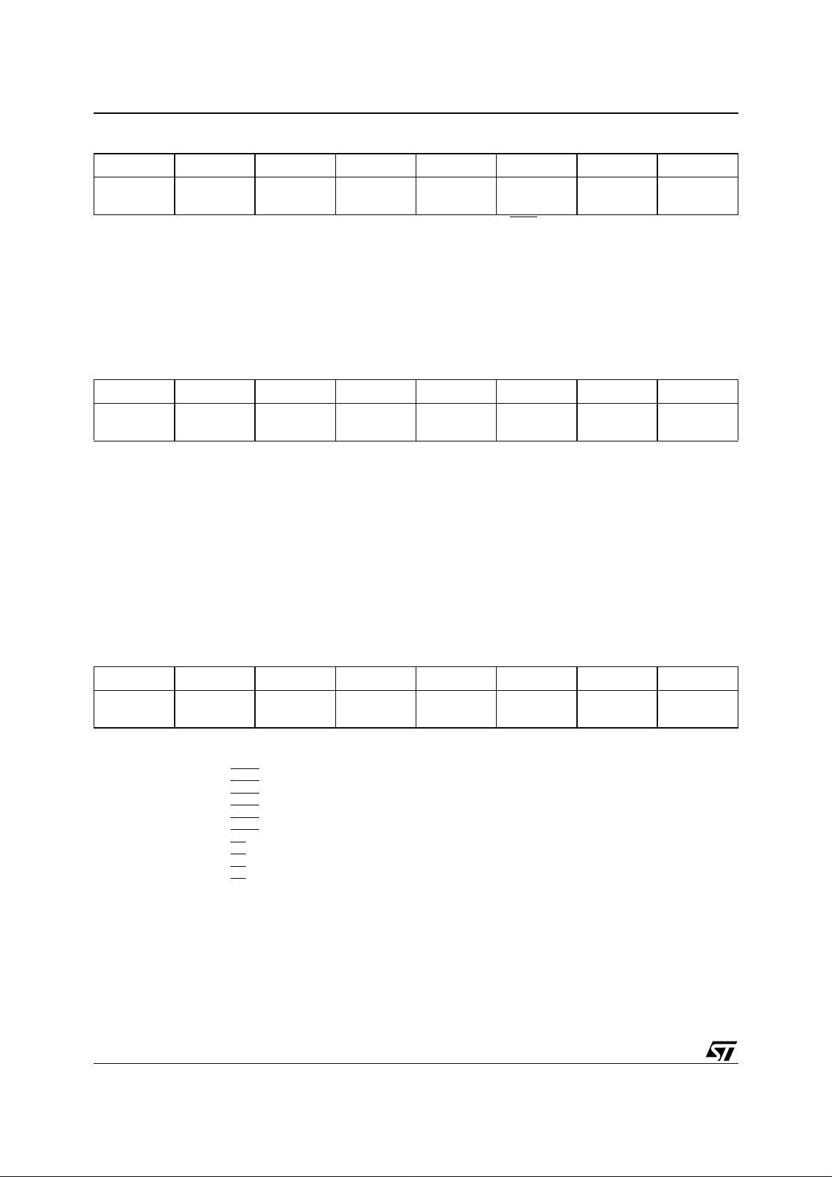
Figure 6. Dat a Po ll i ng F lo wc h a rt
START
READ DQ5 and DQ7
(DQ13 and DQ15)
at Valid Even Address
DQ7
No
(DQ15)
=
Data7
(Data15)
DQ5
(DQ13)
= 1
READ DQ7
(DQ15)
DQ7
(DQ15)
=
Data7
(Data15)
Program
or Erase
Cycle failed
Issue RESET
instruction
Yes
No
Yes
Yes
No
Program
or Erase
Cycle is
complete
AI04920
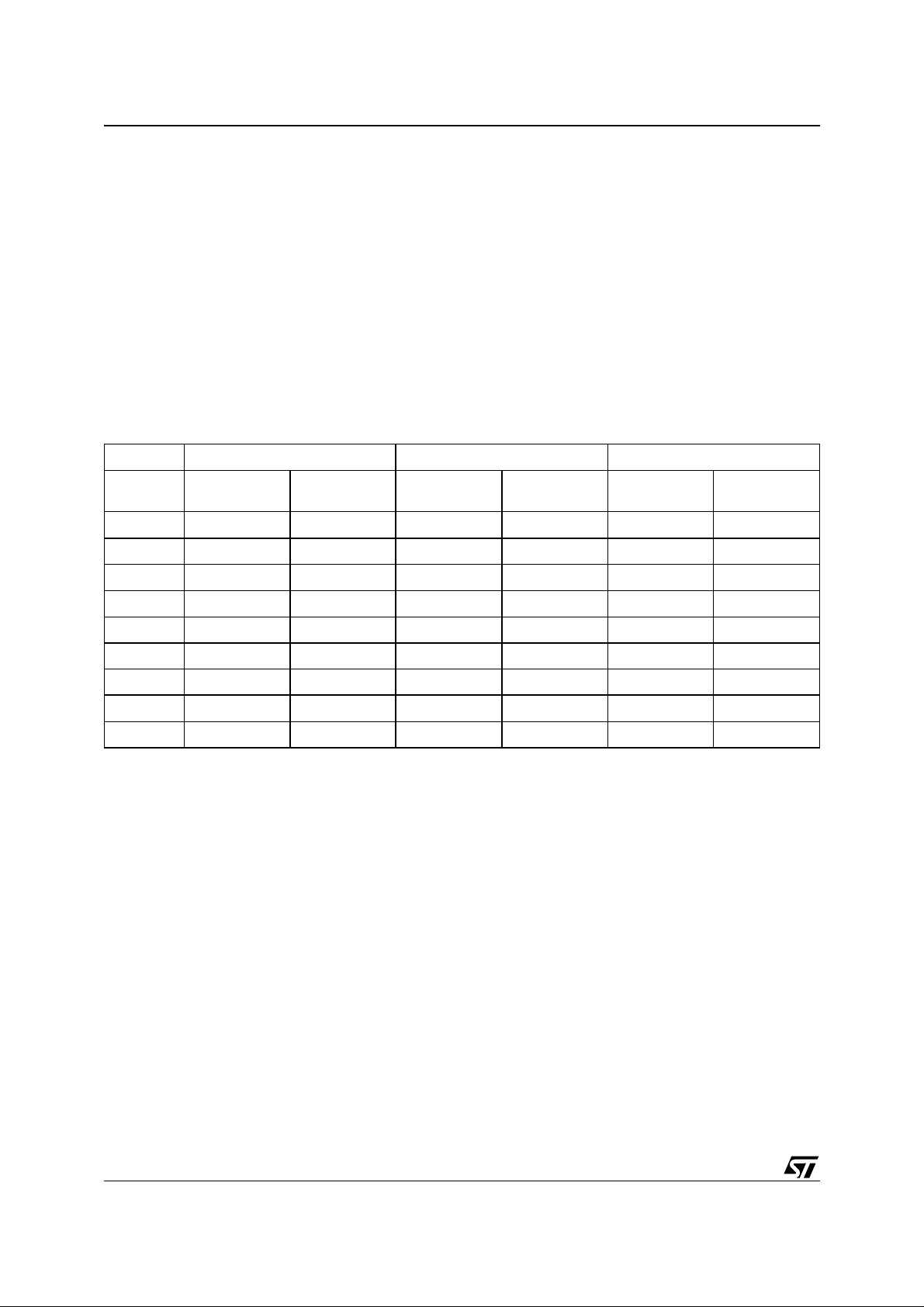
Data Toggle. Checking the Toggle Flag (DQ6/
DQ14) bit is another method of determining whether a Program or Erase cycle is in progress or has
completed. Figure 7 shows t he Data Toggle algorithm.
When the MCU issue s a Program ins truction, the
embedded algorithm within the PSD begins. The
MCU then reads the location to be programmed in
Flash memory to check the status. The Toggle
Flag (DQ6/DQ14 ) bit toggles ea ch time the MCU
25/89
PSD4235G2V
reads this location until the embedded algorithm is
complete. The MCU continues to read this location, checking the Toggle Flag (DQ6/DQ14) bit
and monitoring the Error Flag (DQ5/DQ13) bit.
When the Toggle Flag (DQ6 /DQ1 4) bit stops toggling (two consecutive reads yield the same v alue), and the Error Flag (DQ5/DQ13) bit remains 0,
the embedded a lgorithm is complete. If the Error
Flag (DQ5/DQ13) bit is 1, the MCU should test the
Toggle Flag (DQ6/DQ14) bit again, since the Toggle Flag (DQ6/DQ14) bit may have changed simultaneously with the Error Flag (DQ5/DQ13) bit (see
Figure 7).
Figure 7. Dat a Toggle Flow cha rt
START
READ DQ5 and DQ6
(DQ13 and DQ14)
at Valid Even Address
No
DQ6
(DQ14)
=
Toggle
DQ5
(DQ13)
= 1
READ DQ6
(DQ14)
DQ6
(DQ14)
=
Toggle
Program
or Erase
Cycle failed
Issue RESET
instruction
No
Yes
Yes
No
Yes
Program
or Erase
Cycle is
complete
AI04921
The Error Flag (DQ5/DQ13) bit is set if either an internal time-out occurred while the embedded algorithm attempted to program, or if the MCU
attempted to program a 1 to a bit that was not
erased (not erased is logic 0).
It is suggested (as with all Flash memories) to read
the location again after the embedded programming algorithm has completed, to compare the
word that was written to Flash memory with the
word that was intended to be written.
When using the Data Toggle method after an
Erase cycle, Figure 7 still applies. the Toggle Flag
(DQ6/DQ14) bit toggles until the Erase cycle is
complete. A 1 on the Error Flag (DQ5/DQ13) bit indicates a time-out condition on the Erase cycle, a
0 indicates no error. The MCU can read any even
location within the sector bei ng erased to get t he
Toggle Flag (DQ6/DQ14) bit and the Error Flag
(DQ5/DQ13) bit.
PSDsoft Express generates ANSI C code functions which implement these Data T oggling algorithms.
Unlock Bypass. The Unlock Bypass instruction
allows the system t o program words to the Flash
memories faster than using the standard Program
instruction. The Unloc k Bypass mode is ent ered
by first initiati ng two Unlo ck cycles. T his is fol lowed
by a third Write cycle cont aining the Unlock Bypass command, 20 h (as shown in T able 29). The
Flash memory then enters the Unlock Bypass
mode.
A two-cycle Unlock Bypass Program instruction is
all that is required to program i n this mode. The
first cycle in this instruction contains the Unlock
Bypass Program command , A0h. The second cycle contains the program address and data. A dditional data is programmed in the same manner.
This mode dispense with the initial two Unlock cycles required in the s tandard P rogram instruction,
resulting in faster total programming time.
During the unlock bypass mode, only the Unlock
Bypass Program and Unlock Bypass Reset instructions are valid.
To exit th e Un l o ck Bypass mode, the system must
issue the two-cycle Unlock Bypass Reset instruction. The first cycle must contain the data 90h; the
second cycle the data 00h. A ddresses are Don’t
Care for both cycles. The Flash memory then returns to Read mode.
Erasing Flash Memory
Flash Bulk Erase. The Flash Bulk Erase instruc-
tion uses six Write operat ion s followed by a Read
operation of the status register, as described in
Table 29. If any byte of t he Bulk Erase instruction
is wrong, the Bulk Erase instruction aborts and the
device is reset to the Read Memory mode.
During a Bulk Erase, the memory status may be
checked by reading the Error Flag (DQ5/DQ13)
bit, the Toggle Flag (DQ6/DQ14) bit, and the Data
Polling ( DQ 7/DQ15 ) b it, as de tailed in the sect ion
26/89

PSD4235G2V
entitled “Programming Flash Memory”, on page
25. The Error Flag (DQ5 /DQ13) bit returns a 1 if
there has been an Erase Failure (maximum number of Erase cycles have been exec ut ed ) .
It is not necessary to program the memory with
00h because the PSD automatically does this before erasing to 0FFh.
During execution of the Bulk Erase instruction, the
Flash memory does not accept any instructions.
Flash Sector Erase. The Sector Erase instruction uses six Write operations, as described in Table 29. Additional Flash Sector Erase confirm
commands and Flash m emory sector addresses
can be written subsequently to erase ot her Flash
memory sectors in parallel, wi thout further coded
cycles, if the additional commands are transmitted
in a shorter time than the time-out period of about
100 µs. The input of a new Sector Erase command
restarts the time-out period.
The status of the internal timer can be monitored
through the level of the Erase Time-out Flag (DQ3/
DQ11) bit. If the Erase Time-out Flag (DQ3/DQ11)
bit is 0, the Sector Erase instruc tion has be en received and the time-out p eriod is counting. If the
Erase Time-out Flag (DQ3/DQ11) bit is 1, the
time-out period has expired and the PSD is busy
erasing the Flash memory secto r(s). Before and
during Erase time-out, any i nstruction other than
Suspend Sector Erase and Resume Sector Erase,
abort the cycle that is currently in progress, and reset the device to Read mode. It is not necessary to
program the Flash memory sector with 00h as the
PSD does this automatically before erasing.
During a Sector Erase, the memory status may be
checked by reading the Error Flag (DQ5/DQ13)
bit, the Toggle Flag (DQ6/DQ14) bit, and the Data
Polling ( DQ 7/DQ 15) b it, as de tailed in the sec tion
entitled “Programming Flash Memory”, on page
25.
During execution of the Erase cycle, the Flash
memory accepts only Reset and Suspend Sector
Erase instructions. Erasure of one Flash memory
sector may be suspended, in order to read data
from another Flash memory sector, and t hen resumed .
Suspend Sector Erase. When a Sector Erase
cycle is in progress, the Suspend Sector Erase instruction can be used to suspend the cycle by writing 0B0h to any even address when an
appropriate Sector Select (FS0-FS7 or
CSBOOT0-CSBOOT3) is High. (See Table 29).
This allows reading of data from another Flash
memory sector after the Erase cycle has been
suspended. Suspend Sector Erase is accepted
only during the Flash Sector Erase instruction execution and defaults to Read mode. A Suspend
Sector Erase instruction executed during an Erase
time-out period, in addition to suspending the
Erase cycle, terminates the time out period.
The Toggle Flag (DQ6/DQ14) bit stops toggling
when the PSD internal logic is suspended. The
status of this bit must be m onit ored a t a n address
within the Flash memory sector being erased. The
Toggle Flag (DQ6/DQ14) bit stops toggling between 0.1 µs and 15 µs after the Suspen d Sector
Erase instruction has been executed. The PSD is
then automatically set to Read mode.
If an Suspend Sector Erase instruction was executed, the following rules apply:
– Attempting to read from a Flash memory se ctor
that was being erased outputs invalid data.
– Reading from a Flash memory sect or that was
not
being erased is valid.
– The Flash memory
only responds to Resume Sector Erase and Reset instructions (Read is an operation and is allowed).
– If a Reset instruction is received, data in the
Flash memory sector that was being erased is
invalid.
Resume Sector Erase. If a Suspend Sector
Erase instruction was previously executed, the
Erase cycle may be resumed with this instruction.
The Resume Sector Eras e instruction consists of
writing 030h to any even address while an appropriate Sector Select (FS0-FS7 or CSBOOT0CSBOOT3) is High. (See Table 29.)
Flash Memory Sector Protect
Each secto r o f Pri mary or Se co ndar y Flash memory can be separately p rotected against Program
and Erase cycles. Sector Protection provides additional data security be cause it disables all Program or Erase cycles. This mode can be activated
(or deactivated) through the JTAG-ISP Port or a
Device Programmer.
Sector protection can be selected for each sector
using the PSDsoft Express program. This automatically protects selected sectors when the device is programmed through the JTAG Port or a
Device Programmer. Flash memory sectors can
be unprotected to allow upda ting of t heir contents
using the JTAG Port or a Device Programmer. The
MCU can read (but cannot change) the sector protection bits.
Any attempt to program or erase a protected Flash
memory sector is ignored by the device. The Verify
operation results in a read of the protected data.
This allows a guarantee of the retention of the Protection status.
The sector protection status can be read by the
MCU through the Flash memory protection and
Secondary Flash memory prot ection registers (in
cannot
be programmed, and
27/89
 Loading...