

Page 1
June 2017
DocID030479 Rev 2
1/55
www.st.com
UM2191
User manual
STM32 Nucleo pack for USB Type-C™ and Power Delivery with
the Nucleo-F072RB board and the STUSB1602
Introduction
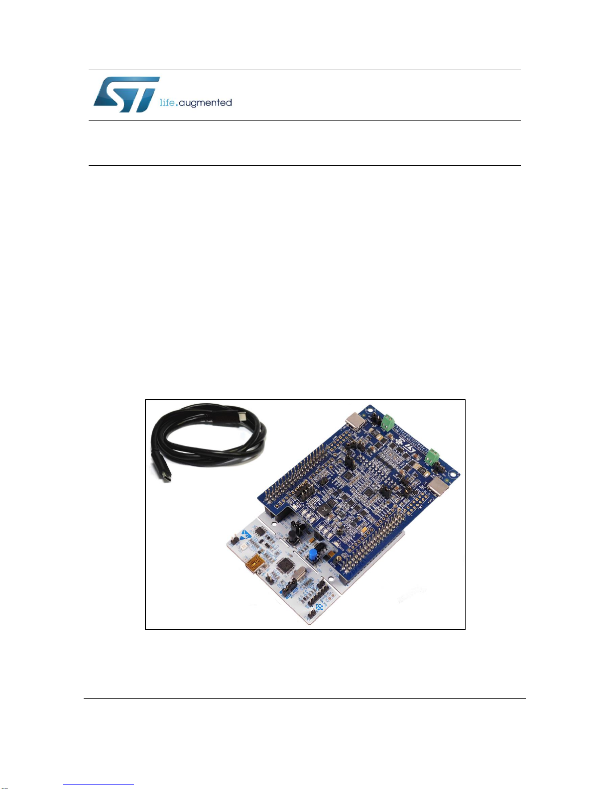
The USB Type-C™ and Power Delivery Nucleo pack P-NUCLEO-USB002 includes:
the NUCLEO-F072RB board
the P-NUCLEO-USB002 expansion board based on the certified STUSB1602 USB Type-C port
controller with PD PHY and BMC driver
a full-featured Type-C cable
These components, together with the X-CUBE-USB-PD certified STM32F0 USB Type-C PD middleware
stack, form a platform for demonstrating USB Type-C and USB Power Delivery (USB PD) capabilities
and facilitating solution development.
The new USB PD protocol expands USB functionality by providing up to 100 W power over the same
cable used for data communication. Devices supporting the protocol are able to negotiate voltage and
current over the USB power pins and define their roles as Provider or Consumer accordingly.
Once the platform is configured, the embedded demonstration firmware can signal cable status
(attached or detached) and orientation information, as well as the role of each of the two ports.
Figure 1: P-NUCLEO-USB002 kit
Page 2

Contents
UM2191
2/55
DocID030479 Rev 2
Contents
1 USB Type-C and Power Delivery .................................................... 6
1.1 Overview ........................................................................................... 6
1.2 Main characteristics .......................................................................... 6
1.3 USB Type-C™ pin map ..................................................................... 7
1.4 Port configurations ............................................................................ 9
1.4.1 Downstream Facing Port (DFP) ......................................................... 9
1.4.2 Upstream Facing Port (UFP) .............................................................. 9
1.4.3 Source or provider .............................................................................. 9
1.4.4 Sink or consumer ................................................................................ 9
1.4.5 Dual Role Power (DRP)...................................................................... 9
1.5 USB-C PD architecture ..................................................................... 9
1.5.1 Device Policy Manager (DPM) ......................................................... 10
1.5.2 Policy Engine (PE) ............................................................................ 10
1.5.3 Protocol Layer (PRL) ........................................................................ 10
1.5.4 Physical layer (PHY) ......................................................................... 10
1.6 CC pins: port termination characteristics ......................................... 11
1.7 Power options ................................................................................. 11
1.8 Cable attachment and detachment detection and orientation ......... 12
1.9 Power negotiation ........................................................................... 13
1.10 Full-featured Type-C™ cable and V
CONN
supply ............................. 14
1.11 Alternate modes and billboard device class .................................... 15
2 System architecture ...................................................................... 17
2.1 System block scheme ..................................................................... 19
2.2 NUCLEO-F072RB STM32 Nucleo board ........................................ 19
2.3 P-NUCLEO-USB002 expansion board ............................................ 21
2.3.1 P-NUCLEO-USB002 expansion board: USB Type-C connectors,
voltage and current sense stage ...................................................................... 24
2.3.2 P-NUCLEO-USB002 expansion board: STUSB1602 USB Type-C
controller 26
2.3.3 P-NUCLEO-USB002 expansion board: V
CONN
switch ...................... 28
2.3.4 P-NUCLEO-USB002 expansion board: VBUS management........... 30
2.3.5 P-NUCLEO-USB002 expansion board: local power management
stage 31
2.3.6 P-NUCLEO-USB002 expansion board: STSAFE secure device ..... 32
2.3.7 P-NUCLEO-USB002 expansion board: USB2.0 .............................. 33
2.3.8 P-NUCLEO-USB002 expansion board: ESD protections ................ 34
Page 3

UM2191
Contents
DocID030479 Rev 2
3/55
2.3.9 P-NUCLEO-USB002 expansion board: connectors ......................... 35
2.3.10 P-NUCLEO-USB002 expansion board: test points .......................... 37
2.3.11 P-NUCLEO-USB002 expansion board: jumpers .............................. 38
2.3.12 P-NUCLEO-USB002 expansion board: user LEDs .......................... 38
2.4 Full-featured Type-C cable .............................................................. 38
3 System setup ................................................................................. 39
3.1 Source power role configuration ...................................................... 39
3.1.1 Using the NUCLEO-F072 on-board voltage regulator ..................... 39
3.1.2 Using an external power supply ....................................................... 39
3.2 Sink power role configuration .......................................................... 40
3.2.1 Using the NUCLEO-F072RB on-board voltage regulator ................ 40
3.2.2 Using an external provider ............................................................... 40
3.3 Dual Role Power configuration ........................................................ 41
3.3.1 Using the NUCLEO-F072RB on-board voltage regulator ................ 41
3.3.2 Using an external power supply ....................................................... 41
4 Ordering information ..................................................................... 42
5 Electrical schematics .................................................................... 43
6 Bill of materials .............................................................................. 48
7 Acronyms and abbreviations ....................................................... 52
8 References ..................................................................................... 53
9 Revision history ............................................................................ 54
Page 4

List of tables
UM2191
4/55
DocID030479 Rev 2
List of tables
Table 1: USB Type-C pinout description .................................................................................................... 8
Table 2: Source CC termination (Rp) requirements ................................................................................. 11
Table 3: Sink CC termination (Rd) requirements ...................................................................................... 11
Table 4: Power options ............................................................................................................................. 12
Table 5: NUCLEO-F072RB solder bridges and resistors to be modified ................................................. 20
Table 6: P-NUCLEO-USB002 expansion board VCONN settings ........................................................... 28
Table 7: P-NUCLEO-USB002 expansion board JP100 and JP101 settings ............................................ 33
Table 8: P-NUCLEO-USB002 expansion board serial communication connection ................................. 36
Table 9: P-NUCLEO-USB002 expansion board test points ..................................................................... 37
Table 10: P-NUCLEO-USB002 expansion board jumpers ....................................................................... 38
Table 11: P-NUCLEO-USB002 expansion board LED signaling ............................................................. 38
Table 12: List of acronyms ........................................................................................................................ 52
Table 13: Document revision history ........................................................................................................ 54
Page 5

UM2191
List of figures
DocID030479 Rev 2
5/55
List of figures
Figure 1: P-NUCLEO-USB002 kit ............................................................................................................... 1
Figure 2: USB plug form factors ................................................................................................................. 7
Figure 3: USB Type-C plug pinout .............................................................................................................. 7
Figure 4: USB Type-C receptacle pinout .................................................................................................... 8
Figure 5: USB power delivery architecture ............................................................................................... 10
Figure 6: Pull up/down CC detection ........................................................................................................ 12
Figure 7: Message flow during power negotiation .................................................................................... 14
Figure 8: Pins available for reconfiguration on the plug of the full-featured cable ................................... 15
Figure 9: Pins available for reconfiguration on the receptacle for direct connect applications ................. 15
Figure 10: The two boards composing the P-NUCLEO-USB002 kit ........................................................ 17
Figure 11: Block scheme of the complete architecture ............................................................................. 19
Figure 12: STM32 Nucleo development board ......................................................................................... 20
Figure 13: STM32 Nucleo board top and bottom view ............................................................................. 21
Figure 14: P-NUCLEO-USB002 expansion board .................................................................................... 22
Figure 15: P-NUCLEO-USB002 expansion board functional blocks ........................................................ 22
Figure 16: P-NUCLEO-USB002 expansion board connectors and jumpers ............................................ 23
Figure 17: P-NUCLEO-USB002 expansion board silkscreen................................................................... 23
Figure 18: P-NUCLEO-USB002 expansion board USB Type-C receptacle and current sensing (port 0)
schematic view .......................................................................................................................................... 24
Figure 19: P-NUCLEO-USB002 expansion board USB Type-C receptacle and Current sensing (port 1)
schematic view .......................................................................................................................................... 25
Figure 20: P-NUCLEO-USB002 expansion board Port 0 Current sensing stage schematic view ........... 25
Figure 21: P-NUCLEO-USB002 expansion board Port 1 Current sensing stage schematic view ........... 26
Figure 22: STUSB1602 front end for Port 0 ............................................................................................. 27
Figure 23: P-NUCLEO-USB002 expansion board: JP000 and JP001 jumper settings to provide VCONN
through the local voltage regulator ........................................................................................................... 29
Figure 24: P-NUCLEO-USB002 expansion board Port 0 schematic view of the VBUS management
mechanism ................................................................................................................................................ 30
Figure 25: P-NUCLEO-USB002 expansion board Port 1 schematic view of the VBUS management
mechanism ................................................................................................................................................ 30
Figure 26: P-NUCLEO-USB002 expansion board: schematic view of the load switches of the local
power management .................................................................................................................................. 31
Figure 27: P-NUCLEO-USB002 expansion board: schematic view of the local DC-DC converter .......... 32
Figure 28: P-NUCLEO-USB002 expansion board: STSAFE-A100 schematic view ................................ 32
Figure 29: P-NUCLEO-USB002 expansion board: JP100 and JP101 connectors for USB 2.0
configurations ............................................................................................................................................ 34
Figure 30: P-NUCLEO-USB002: CN13 and C14 connector pinout .......................................................... 35
Figure 31: P-NUCLEO-USB002: CN4 connector ..................................................................................... 36
Figure 32: P-NUCLEO-USB002 expansion board CN2_1 and CN3_TX pin indications ......................... 37
Figure 33: P-NUCLEO-USB002 mounting orientation .............................................................................. 39
Figure 34: P-NUCLEO-USB002 expansion board circuit schematic - global view ................................... 43
Figure 35: P-NUCLEO-USB002 expansion board circuit schematic - MCU interface ............................. 43
Figure 36: P-NUCLEO-USB002 expansion board circuit schematic - STUSB1602 front end Port0 ....... 44
Figure 37: P-NUCLEO-USB002 expansion board circuit schematic - STUSB1602 front end Port1 ....... 44
Figure 38: P-NUCLEO-USB002 expansion board circuit schematic - local power .................................. 45
Figure 39: P-NUCLEO-USB002 expansion board circuit schematic - local voltage supply ..................... 45
Figure 40: P-NUCLEO-USB002 expansion board circuit schematic - Type-C Connector 0 .................... 46
Figure 41: P-NUCLEO-USB002 expansion board circuit schematic - Type-C Connector 1 .................... 46
Figure 42: P-NUCLEO-USB002 expansion board circuit schematic - Current Sensing C0 ..................... 47
Figure 43: P-NUCLEO-USB002 expansion board circuit schematic - Current Sensing C1 ..................... 47
Figure 44: P-NUCLEO-USB002 expansion board circuit schematic - security ........................................ 47
Page 6

USB Type-C and Power Delivery
UM2191
6/55
DocID030479 Rev 2
1 USB Type-C and Power Delivery
1.1 Overview
The USB Type-C™ and Power Delivery technologies simplify development and enhance
user experience; the new reversible USB Type-C connector insertion is more intelligent and
user friendly.
These technologies offer a smart connector able to carry all the necessary data (including
video) as well as negotiate up to 100 W supply or charge connected equipment according
to the Power Delivery protocol.
Less cables, less connectors and universal chargers are among the final objectives.
The USB Type-C connector supports up to 15 W (5 V at 3 A), which rises to 100 W (up to
20 V at 5 A) adopting the USB Power Delivery feature.
1.2 Main characteristics
The USB Implementer Forum (USB-IF) introduces these complementary specifications:
1. the USB Type-C™ receptacle, plug and cable specification rev. 1.2
2. the USB Power Delivery (PD) specification rev. 2.0 that allows two PD compliant
entities to exchange up to 100 W during their negotiations.
Any system embedding a USB Type-C receptacle or plug which is designed to implement a
USB Power Delivery application such as a single port device, a multi-port hub or a simple
cable is based on these specifications.
The connector is intended for a wide range of charging applications like computers,
displays and mobile phones, with all the advanced features of PD:
power role negotiation
power sourcing and consumption level negotiation
electronically marked cable identification
vendor-specific message exchange
alternate-mode negotiation, allowing different communication protocols to be routed
onto the reconfigurable pins of the USB Type-C connectors.
The cables use the same male connector on both ends.
Page 7
UM2191
USB Type-C and Power Delivery
DocID030479 Rev 2
7/55
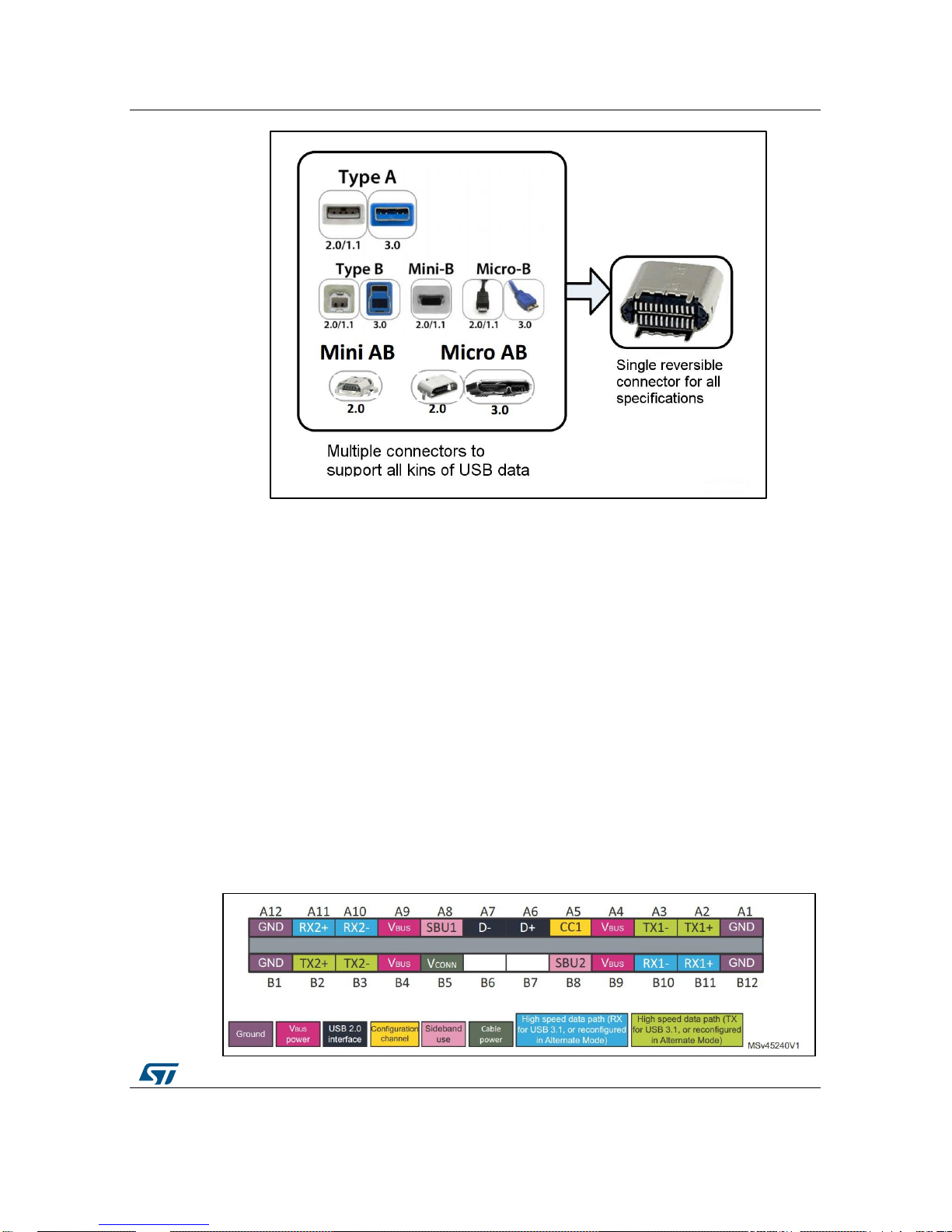
Figure 2: USB plug form factors
The new USB Type-C covers all the features provided by the previous generation USB
plugs in a single connector, rendering USB usage easier and more flexible. It supports all
protocols from USB2.0 onward, including power capability.
The USB Type-C connection allows ports to operate in host-mode only, device-mode only
or dual-role. Both data and power roles can be independently and dynamically swapped
using the USB PD protocol.
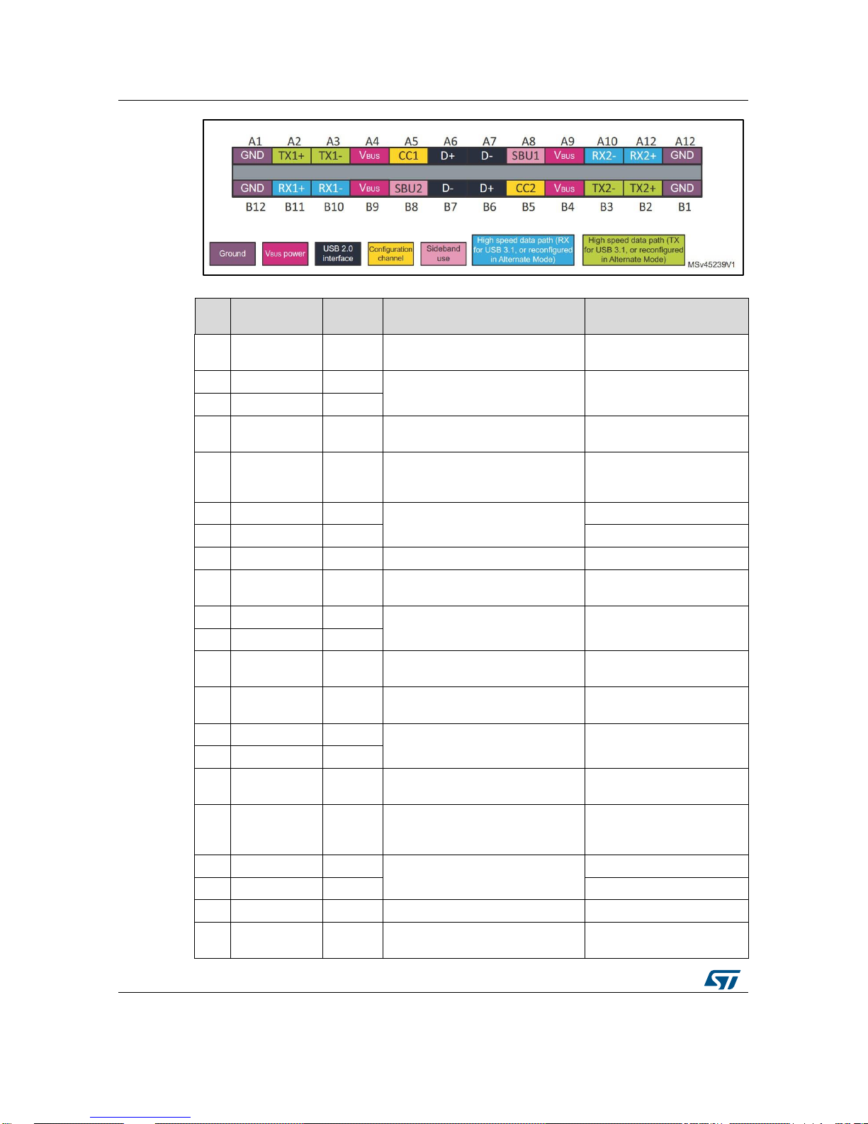
1.3 USB Type-C™ pin map
USB Type-C™ plugs and receptacles are 24-pin connectors with two groups of pin
connections arranged so as to ensure pinout reversibility for any connection.
The symmetrical connections: are
eight power pins: V
BUS
/GND
USB2.0 differential pairs (D+/D-)
The asymmetrical connections are:
two sets of Tx/Rx signal paths supporting USB3.1 data rates
two configuration channels (CC lines) for the discovery, configuration and
management of USB Type-C power delivery features
two sideband use (SBU lines) signals for analog audio modes; may be used by
alternate mode.
Figure 3: USB Type-C plug pinout
Page 8
USB Type-C and Power Delivery
UM2191
8/55
DocID030479 Rev 2
Figure 4: USB Type-C receptacle pinout
Table 1: USB Type-C pinout description
Pin
Receptacle
signal
Plug
signal
Description
Comment
A1
GND
GND
Ground return
Can be up to 5 A split into
four pins
A2
TX1+
TX1+
USB3.1 data lines or Alternate
10-Gbyte TX differential
pair in USB 3.1
A3
TX1-
TX1-
A4
V
BUS
V
BUS
Bus power
Max power is 100 W (20 V
at 5 A) split into four pins
A5
CC1 or V
CONN
CC
Configuration channel or power for
active or electronically marked
cable
In VCONN configuration,
max. power is 1 W
A6
D+
D+
USB2.0 datalines
-
A7
D-
D-
-
A8
SBU1
SBU1
Sideband Use (SBU)
Alternate mode only
A9
V
BUS
V
BUS
Bus power
Max power is 100 W split
into four pins
A10
RX2-
RX2-
USB3.1 datalines or Alternate
10-Gbyte RX differential
pair in USB 3.1
A11
RX2+
RX2+
A12
GND
GND
Ground return
Can be up to 5 A split into
four pins
B1
GND
GND
Ground return
Can be up to 5 A split into
four pins
B2
TX2+
TX2+
USB3.1 datalines or Alternate
10-Gbyte RX differential
pair in USB 3.1
B3
TX2-
TX2-
B4
V
BUS
V
BUS
Bus power
Max power is 100 W split
into four pins
B5
CC2 or V
CONN
V
CONN
Configuration channel or power for
active or electronically marked
cable
In V
CONN
configuration,
max. power is 1 W
B6
D+
-
USB2.0 datalines
-
B7
D-
- - B8
SBU2
SBU2
Sideband Use (SBU)
Alternate mode only
B9
V
BUS
V
BUS
Bus power
Max power is 100 W split
into four pins
Page 9
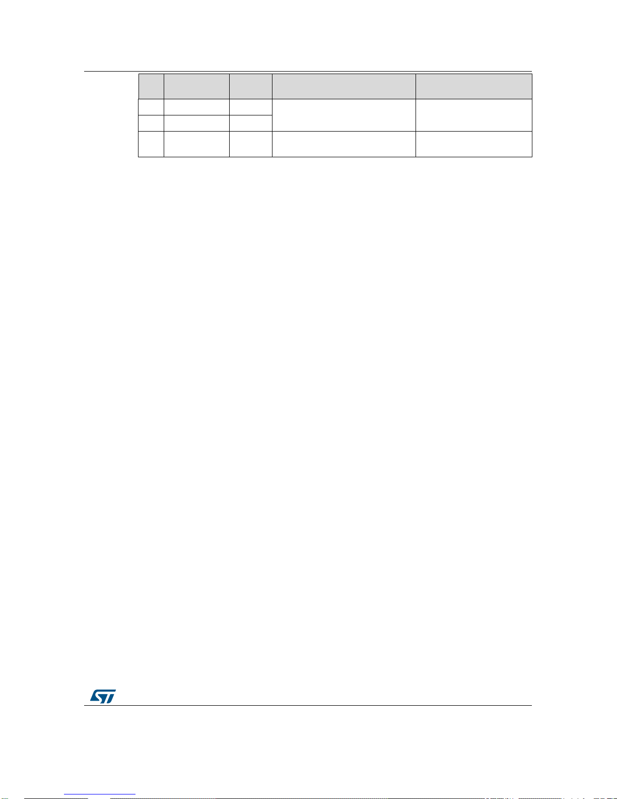
UM2191
USB Type-C and Power Delivery
DocID030479 Rev 2
9/55
Pin
Receptacle
signal
Plug
signal
Description
Comment
B10
RX1-
RX1-
USB3.1 datalines or Alternate
10-Gbyte RX differential
pair in USB 3.1
B11
RX1+
RX1+
B12
GND
GND
Ground return
Can be up to 5 A split into
four pins
1.4 Port configurations
As stated in the USB Type-C™ and USB Power Delivery specifications, a data role (host or
device) and a power role (source, sink or DRP) can be assigned to each port. Both data
and power roles can be independently and dynamically swapped according to rules and
procedures established by the specifications.
1.4.1 Downstream Facing Port (DFP)
The downstream facing port is associated with the flow of data in a USB connection. It is
usually the port on a host or hub which devices connect to.
In its initial state, the DFP must be able to supply V
BUS
and V
CONN
and support data.
1.4.2 Upstream Facing Port (UFP)
The upstream facing port is associated with the data flow in a USB connection. It
represents the port on a device or a hub that connects to a host or the DFP of a hub. In its
initial state, UFP sinks V
BUS
and supports data (e.g., display).
1.4.3 Source or provider
This port must source power over V
BUS
(5 V to 20 V and up to 5 A), and most commonly
belongs to a host or hub DFP. A provider must assert an Rp resistor (pull-up resistor, See
Figure 5: "USB power delivery architecture") on CC pins (configuration channel pins, see
Section 1.6: "CC pins: port termination characteristics").
1.4.4 Sink or consumer
This port is able to sink power over V
BUS
, making use of power (from 5 V to 20 V and up to
5 A), most commonly embedded on a device or UFP. A Consumer must assert an Rd
resistor (pull-down resistor: see Figure 5: "USB power delivery architecture") on CC pins.
1.4.5 Dual Role Power (DRP)
A dual role power USB port can operate as a source or a sink. The initial role of the port
may be fixed or may alternate between the two port states.
Initially, when operating as a source, the port also assumes the role of DFP; when
operating as a sink, the port takes the role of UFP.
The port role may be changed dynamically to reverse power.
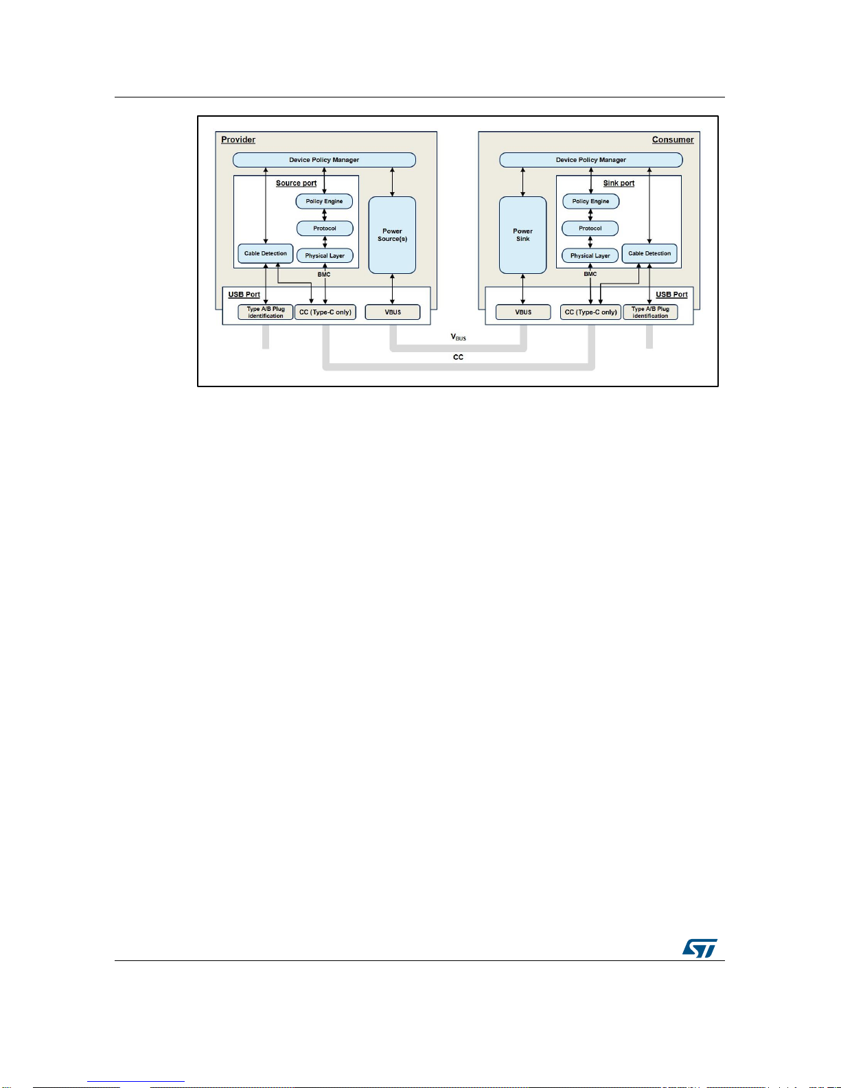
1.5 USB-C PD architecture
The USB Power Delivery specification defines the stack architecture with all its layers
managing a PD device.
Page 10
USB Type-C and Power Delivery
UM2191
10/55
DocID030479 Rev 2
Figure 5: USB power delivery architecture
As per the USB Power Delivery protocol, a USB DFP is initially a Source and a USB UFP is
initially a Sink. When these two entities are connected between them, they start to
communicate by means of the configuration channel (CC), while the Source supplies the
Sink through the V
BUS
path. Although USB-PD enables the Source/Sink and the DFP/UFP,
the roles may be swapped every time the application requests it.
1.5.1 Device Policy Manager (DPM)
The device policy manager deals with the USB Power Delivery resources used by one or
more ports on the basis of the local device policy. It interacts with the policy engines and
cable detection entities of the device to implement the local policies for each port.
1.5.2 Policy Engine (PE)
The policy engine interacts directly with the DPM to determine which local policy to apply.
Its role is to drive the message sequences according to the sent message and its expected
response.
It allows power negotiation by establishing an explicit contract for power exchange. The
acceptance or the refusal of a request depends on the response of the DPM with respect to
a specific power profile.
The PE also handles the flow of vendor defined messages, allowing the discovery, entry
and exit of modes supported by the provider and consumer sides.
1.5.3 Protocol Layer (PRL)
The protocol layer drives message construction, transmission, reception and
acknowledgment. It allows the monitoring of message flows and the detection of
communication errors.
1.5.4 Physical layer (PHY)
The physical layer is responsible for sending and receiving messages across the CC wire.
It consists of a transceiver that superimposes a BMC signal on the wire. It is responsible for
managing data over the wire, avoiding collisions and detecting errors in the messages
using a Cyclic Redundancy Check (CRC).
Page 11
UM2191
USB Type-C and Power Delivery
DocID030479 Rev 2
11/55
1.6 CC pins: port termination characteristics
The configuration channel (CC) pins are used in the discovery, configuration and
management of connection across a USB Type-C™ cable, as well as a communication
channel for the PHY layer of the USB Power Delivery.
There are two CC pins in each receptacle, but only one is connected through the cable to
establish communication. The other pin can be re-assigned as the V
CONN
pin for powering
electronics in the USB Type-C™ plug of electronically-marked cables.
Specific Rd and Rp resistor values connected to CC pins allow single role or dual role
system configuration. The attachment and orientation detection operations are carried out
through CC lines through these resistors:
a source must assert Rp pull-up resistors on both CC1 and CC2
a sink must assert Rd pull-down resistors on both CC pins
a dual role power (DRP) is equipped with both Rp pull-up resistors and Rd pull-down
resistors on its CC pins and is able to dynamically assert the appropriate resistors
when the role is fixed by the application according to the operated power role.
A full-featured USB Type-C cable must assert Ra pull-down resistors on the V
CONN
pin.
The following table provides the values to be used for Rp or current source.
Table 2: Source CC termination (Rp) requirements
Source
Current Capability
Current Source
to 1.7 V - 5.5 V
Rp pull-up
to 3.3 V ±5%
Rp pull-up
to 4.75 V - 5.5 V
Default USB power
80 µA ±20%
36 kΩ ±20%
56 kΩ ±20%
1.5 A at 5 V
180 µA ±8%
12 kΩ ±5%
22 kΩ ±5%
3.0 A at 5 V
330 µA ±8%
4.7 kΩ ±5%
10 kΩ ±5%
Rp resistors connected to both CC pins may be pulled-up to 3.3 V or 5 V. The resistor
value is chosen on the basis the device port supplying capability. Moreover, if the source
role is operated, the Rp resistors can be replaced by current sources.
The following table provides the values to be used for Rd or Sink CC termination.
Table 3: Sink CC termination (Rd) requirements
Rd setting
Nominal Value
Max Voltage on pin
Power Capability detection
±20% voltage clamp
1.1 V
1.32 V
No
±20% resistor to GND
5.1 kΩ
2.18 V
No
±10% resistor to GND
5.1 kΩ
2.04 V
Yes
Rd resistors may be implemented in multiple ways.
1.7 Power options
Regarding power exchange, every platform equipped with a Type-C™ connector but
without power delivery must be able to support 5 V with one of the specific current
capabilities. When power delivery is supported and the design is specifically optimized for
managing high power loads, the same platform may support up to 20 V at 5 A (100 W).
Page 12
USB Type-C and Power Delivery
UM2191
12/55
DocID030479 Rev 2
Table 4: Power options
Mode of operation
Nominal
voltage
Maximum
current
Maximum
power
Note
USB 2.0
5 V
500 mA
2.5 W
Default current based on
specification
USB 3.1
900 mA
4.5 W
USB BC1.2
up to 1.5 A
7.5 W
Legacy charging
USB Type-C™
current at 1.5 A
1.5 A
Support high power devices
USB Type-C™
current at 3 A
3 A
15 W
USB PD
up to 20 V
up to 5 A
100 W
Directional control and power
level management
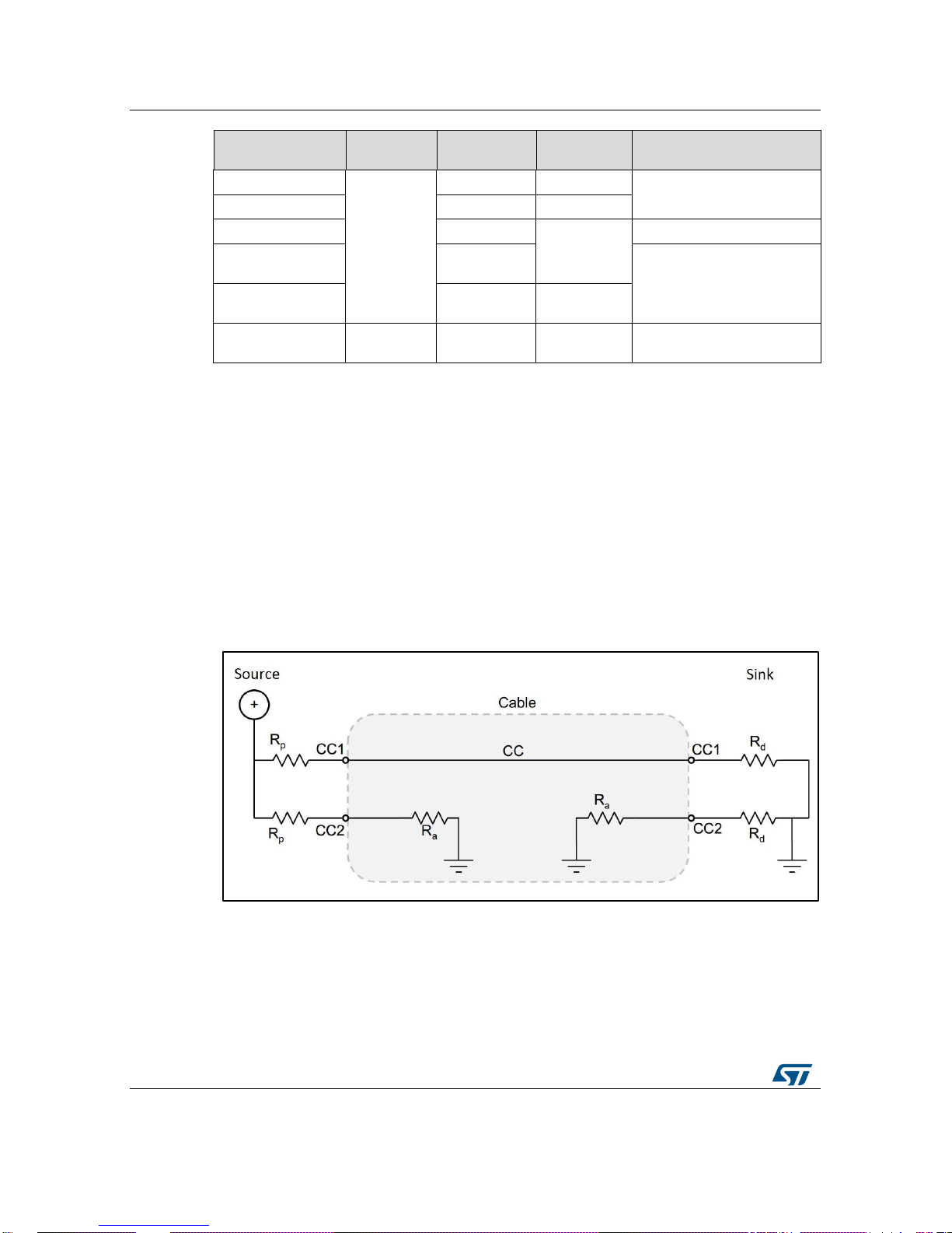
1.8 Cable attachment and detachment detection and orientation
As stated in the USB Power Delivery specification, it is mandatory to determine the
orientation of an attachment; i.e., when one of the two CC pins detects a valid Rp/Rd
connection.
To detect an attachment, the source monitors both CC pins.
The pins are floating when nothing is attached, but when the sink is attached via the cable,
one CC line of the source is directly pulled-down (through the sink Rd), signalling that a
connection has been made (see Figure 6: "Pull up/down CC detection").
Hence, once connection is established, a voltage divider is set between source pull-up
resistor Rp and sink pull-down resistor Rd, fixing the voltage level on the CC line for the
communication signals.
Figure 6: Pull up/down CC detection
At the same time, the orientation of the plug, and consequently of the cable, is defined
according to which CC line (CC1 or CC2) detects a valid resistance after the attach event.
The figure above shows an unflipped cable orientation.
Moreover, the full-featured cable, exposing an Ra resistor, connects the V
CONN
pins to
ground.
Page 13

UM2191
USB Type-C and Power Delivery
DocID030479 Rev 2
13/55
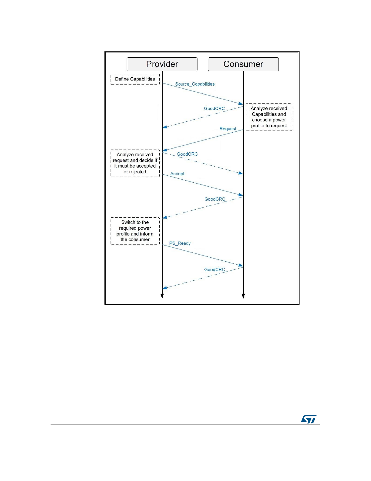
1.9 Power negotiation
When a connection is made and the respective roles have been assigned, the source and
the sink negotiate a contract for the power objects: the selected configuration channel (CC)
allows them to establish communication and negotiate the power according to the protocol
described in USB Power Delivery specification.
Originally, all the devices equipped with USB Type-C™ are able to provide up to 15 W (5 V
and up to 3 A) power via the V
BUS
path, but every subsequent request for delivering or
receiving power from 15 W to 100 W (5 V at 3 A to 20 V at 5 A) must be negotiated
according to the USB Power Delivery protocol.
The messages exchanged between a source (provider) and sink (consumer) are illustrated
in Figure 7: "Message flow during power negotiation".
1. Initially, the source dispatches a Source_Capabilities message to inform the port
partner (sink) of its power capabilities.
2. The sink then sends a Request for one of the advertised power profiles.
3. The source accepts or rejects this request according to its power balance.
4. If confirmed, the source sends an Accept to the sink
5. The source then switches to the requested power profile and sends a PS_Ready
confirmation message.
Each received message is acknowledged with a GoodCRC to confirm correct reception.
Incorrect reception should be ignored and persistent communication errors should trigger a
soft reset to reset protocol parameters and re-establish communication. If the error
persists, a hard reset is performed.
Page 14
USB Type-C and Power Delivery
UM2191
14/55
DocID030479 Rev 2
Figure 7: Message flow during power negotiation
1.10 Full-featured Type-C™ cable and V
CONN
supply
Full-featured Type-C™ cables are Type-C™ to Type-C™ cables that support USB2.0 and
USB3.1 data operation, and include sideband use (SBU) wires.
All USB full-featured Type-C cables must be electronically marked and must provide 800 Ω
to 1.2 kΩ impedance (Ra) that connects the assigned V
CONN
pin to ground.
When a full-featured cable is attached to a source, the source must provide a V
CONN
(5 V
default) to supply it (valid voltage range is 3 V to 5.5 V).
Up to 1 W may be drawn from V
CONN
to power the ICs in the plug, necessary to implement
electronically-marked cables and V
CONN
-powered accessories.
Page 15
UM2191
USB Type-C and Power Delivery
DocID030479 Rev 2
15/55
The V
CONN
is systematically assigned to the free CC pin of the receptacle after a connection
is established: the CC pins can be monitored to verify a valid Rp/Ra connection and then
the V
CONN
supply is routed by the source to the checked pin.
Since all the full-featured Type-C™ cables are reversible, both CC pins in the receptacle
must be able to assume the role of CC and V
CONN
on cable insertion.
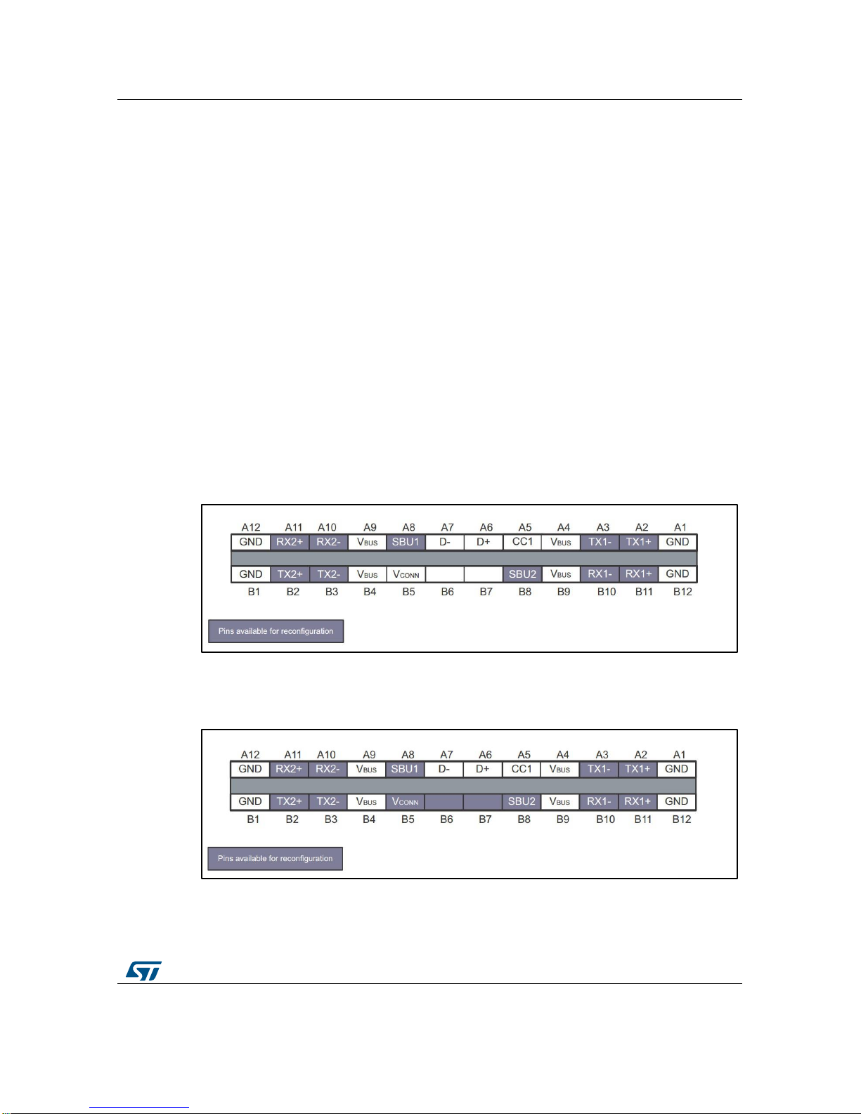
1.11 Alternate modes and billboard device class
The USB Power Delivery specification supports alternate mode (Alt Mode) to transfer highspeed data over Type-C™ cables using protocols like:
High-Definition Multimedia Interface (HDMI)
DisplayPort (DP)
Peripheral Component Interconnect Express (PCI Express)
Ethernet over twisted pair (Base-T Ethernet)
Mobile High-Definition Link (MHL)
The adoption of alternate mode lets Type-C hosts and devices incorporate additional
functionality, exploiting USB PD structured vendor defined messages (Structured VDMs) to
manage typical display controller selection mechanisms: discover, enter and exit.
As alternate modes do not traverse the USB hub topology, they may only be used between
a directly connected host and device.
Structured VDMs may also be used for re-assignment of the pins that the USB Type-C
connector exposes.
Figure 8: Pins available for reconfiguration on the plug of the full-featured cable
The following figure shows the pins available for reconfiguration with direct connect
applications. There are three more pins because this configuration is not limited by the
cable wiring.
Figure 9: Pins available for reconfiguration on the receptacle for direct connect applications
Where no equivalent USB functionality is implemented, the device must provide a USB
interface exposing a USB billboard device class to identify the device. This is not required
for non-user facing modes (e.g., diagnostic modes).
Page 16

USB Type-C and Power Delivery
UM2191
16/55
DocID030479 Rev 2
The USB billboard device class definition describes how to communicate the alternate
modes supported by a device container to a host system, including string descriptors that
provide supporting information in a human-readable format.
Page 17
UM2191
System architecture
DocID030479 Rev 2
17/55
2 System architecture
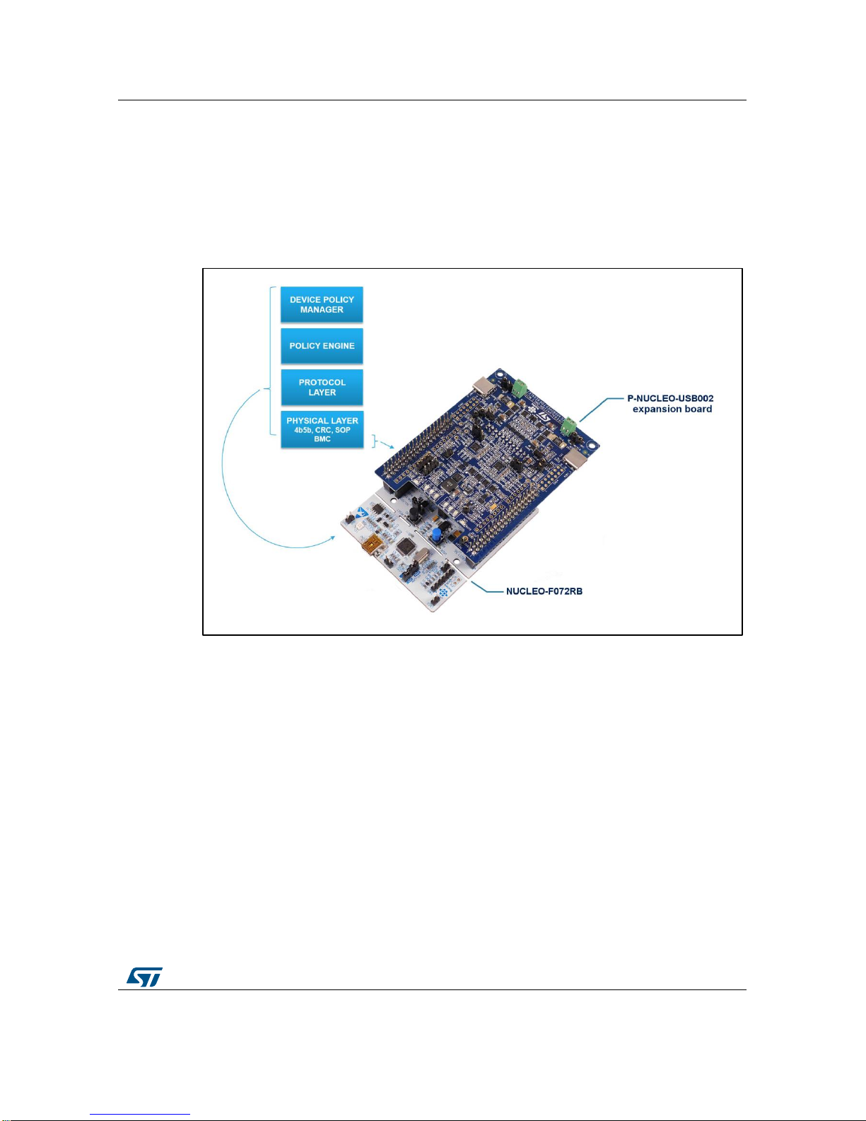
The P-NUCLEO-USB002 USB Type-C™ and power delivery kit includes:
1. a NUCLEO-F072RB development board acting as the control board running the stack
2. a P-NUCLEO-USB002 expansion board acting as a Type-C and Power Delivery
interface, with two STUSB1602 Type-C PD controllers
3. A full-featured and certified USB Type-C cable
Figure 10: The two boards composing the P-NUCLEO-USB002 kit
The P-NUCLEO-USB002 USB Type-C and Power Delivery expansion board is equipped
with:
two DRP USB Type-C™ ports managed by two STUSB1602 Type-C port controllers
optional V
BUS
current sensing (and discrete voltage monitoring)
dedicated power connector to interface with an external power supply (not included) to
provide different profiles as well as VCONN (5V), if necessary
on-board power management able to provide internal supply voltages
six status-control LEDs for USB-PD port purposes, a user LED and a power LED
USB 2.0 interface capability available on both Type-C portsthere is only one USB 2.0
controller, which can be mapped to either port or in pass-through configuration.
RoHS compliant
PCB type and size:
PCB material: FR4
four-layer architecture
copper thickness: 35 µm
The NUCLEO-F072RB board includes:
Page 18

System architecture
UM2191
18/55
DocID030479 Rev 2
an STM32F072RBT6 32-bit microcontroller based on ARM® Cortex®-M0 with 128-
Kbytes of Flash memory, 16-Kbytes of SRAM and a USB 2.0 full speed data interface
in a LQFP64 package
extension resources:
Arduino Uno revision 3 connectivity
ST morpho extension pin headers for full access to all STM32 I/Os
on-board ST-LINK/V2-1 debugger/programmer with SWD connector:
selection-mode switch to use the kit as a standalone ST-LINK/V2-1
flexible board power supply:
USB VBUS on Type-B connector or external source
Power management access point
LEDs:
USB communication (LD1)
user LED (LD2)
power LED (LD3)
push buttons:
USER
RESET
USB re-enumeration capability; interfaces supported on USB:
Virtual Com port
Mass storage
Debug port
Supported by various integrated development environments (IDEs):
IAR™
Keil®
GCC-based IDEs
The NUCLEO-F072RB included in the kit has a different solder bridge
configuration with respect to the default one (see Table 5: "NUCLEO-F072RB
solder bridges and resistors to be modified")
Page 19

UM2191
System architecture
DocID030479 Rev 2
19/55
2.1 System block scheme
Figure 11: Block scheme of the complete architecture
2.2 NUCLEO-F072RB STM32 Nucleo board
The STM32 Nucleo board provides an affordable and flexible way for solution and
prototype development with any of STM32 microcontroller lines.
The board STM32F072RBT6 32-bit microcontroller is based on the ARM® Cortex®-M0 with
128 Kb Flash memory and 16 Kb SRAM.
The Arduino™ connectivity support and ST morpho headers make it easy to expand with a
wide range of specialized expansion boards.
Separate probes are not required as it integrates the ST-LINK/V2-1 debugger/programmer.
The STM32 Nucleo board comes with the comprehensive STM32 HAL software library
together with various packaged software examples.
Visit http://www.st.com/stm32nucleo for more information.
Page 20

System architecture
UM2191
20/55
DocID030479 Rev 2
Figure 12: STM32 Nucleo development board
The solder bridge configuration on the NUCLEO-F072RB Nucleo board is customized to
support USB PD applications (see Table 5: "NUCLEO-F072RB solder bridges and resistors
to be modified" and Figure 13: "STM32 Nucleo board top and bottom view").
For further information, please refer to user manual UM1724 STM32 Nucleo-64 boards on
www.st.com.
Table 5: NUCLEO-F072RB solder bridges and resistors to be modified
Bridge
reference
State
Description
SB13
OFF
PA2 and PA3 on STM32F103CBT6 (ST-LINK MCU) are disconnected from
PA3 and PA2 of the STM32F072RBT6 MCU.
SB14
SB15
OFF
The SWO signal is not connected to PB3 on STM32F072RBT6 MCU.
SB21
OFF
Green user LED LD2 is not connected to PA5 on STM32F072RBT6 MCU.
R34
OFF
LSE not used: PC14 and PC15 used as GPIOs instead of low speed clock.
R36
SB48
ON
SB49
SB62
ON
To connect another USART (not the default USART2) to STLINK MCU,
using flying wires between ST morpho connector and CN3.
SB13 and SB14 should be OFF.
SB63
Page 21

UM2191
System architecture
DocID030479 Rev 2
21/55
Figure 13: STM32 Nucleo board top and bottom view
2.3 P-NUCLEO-USB002 expansion board
The P-NUCLEO-USB002 expansion board consists of different stages for specific aspects
of the power delivery protocol. It embeds two USB Type-C™ ports, each containing the
following functional blocks:
an STUSB1602 Type-C port controller
V
BUS
management stage
voltage and current measurement circuitry
a V
CONN
selector
status LEDs
ESD protections
The P-NUCLEO-USB002 expansion board local voltage regulator interacts with both of
V
BUS
management blocks.
Page 22

System architecture
UM2191
22/55
DocID030479 Rev 2
Figure 14: P-NUCLEO-USB002 expansion board
The USB selectors (JP100, JP101) allow use of the USB2.0 peripheral provided by the
microcontroller, alternately on port 0 and on port 1, as well as allowing a pass-through
topology connecting the USB pins of the two Type-C ports.
The main functional blocks regarding USB-C PD applications are shown below
Figure 15: P-NUCLEO-USB002 expansion board functional blocks
Page 23

UM2191
System architecture
DocID030479 Rev 2
23/55
The connectors and jumpers regarding USB-C PD applications are shown below.
Figure 16: P-NUCLEO-USB002 expansion board connectors and jumpers
Figure 17: P-NUCLEO-USB002 expansion board silkscreen
Page 24

System architecture
UM2191
24/55
DocID030479 Rev 2
2.3.1 P-NUCLEO-USB002 expansion board: USB Type-C connectors,
voltage and current sense stage
The two USB Type-C™ CN0 and CN1 connectors on the P-NUCLEO-USB002 expansion
board represent port 0 and port 1 respectively.
When a port acts as a power provider, it can supply an external device connected via a
USB Type-C™ cable; the same port can receive power if it is set as a consumer.
Figure 18: P-NUCLEO-USB002 expansion board USB Type-C receptacle and current sensing
(port 0) schematic view
DM
DM
DP
PORT0 USB 2. 0 + ESD
DP
A7
A6
B6
B7
USBD0
USBD1
USBD[0..1]
A7
A6
B7
B6
TX1+
RX1+
SBU1
TX2+
RX2-RX2+
TX2-
RX1-
TX1SBU2
TX2-
RX1-
SBU2
RX1+
TX2+
TX1+
SBU1
TX1-
RX2RX2+
CC2
CC1
ISENSE
VBUS
USBD[0..1]
VSENSE
VBUSVBUS
0 0
0
0
0
0 0
D601
SMM4F24A
R603
8.2k
D602
ESDALC5-1BF4
U600
USBLC6-2
I/O2
3
GND
2
I/O1
1
I/O3
4
VBUS
5
I/O4
6
C607
100nF
R604
1.5k
D603
ESDALC5-1BF4
08_CURRENT SENSING Port0
08_CURRENT SENSING Port0
V+
OUT
V-
CN11
2Way
1
2
R605
0.005
TP600
TEST POINT
1
CN13
Alt. Mode Conn. N.M.
1 2
3 4
5 6
7 8
9 10
11 12
13 14
CN0
USB Type-C Receptacle
B12
GND4
B11
RX1+
B10
RX1-
B9
VBUS4
B8
SBU2
B7
D-2
B6
D+2
B5
CC2
B4
VBUS3
B3
TX2-
B2
TX2+
B1
GND3
GND1
A1
TX1+
A2
TX1-
A3
VBUS1
A4
CC1
A5
D+1
A6
D-1
A7
SBU1
A8
VBUS2
A9
RX2-
A10
RX2+
A11
GND2
A12
C606
4.7uF
Page 25

UM2191
System architecture
DocID030479 Rev 2
25/55
Figure 19: P-NUCLEO-USB002 expansion board USB Type-C receptacle and Current sensing
(port 1) schematic view
The STUSB1602 monitors the V
BUS
voltage on the USB Type-C receptacle via its
VBUS_SENSE input pin and alerts the MCU if an undervoltage or overvoltage condition is
detected.
The V
BUS
operating range is defined by a high and a low voltage threshold above and
below the nominal V
BUS
target value. Valid V
BUS
voltage and operating thresholds can be
changed via the I²C interface.
Each port is also equipped with a dedicated current-sensing stage.
Figure 20: P-NUCLEO-USB002 expansion board Port 0 Current sensing stage schematic view
DM
DM
DP
PORT1 USB 2.0 + ESD
DP
B7
B6
USBD0
USBD1
USBD[0..1]
A7
A6
A7
A6
B6
B7
TX1+
RX1+
SBU1
TX2+
RX2-RX2+
TX2-
RX1-
TX1SBU2
RX1+
TX2+
TX2-
RX1- TX1-
SBU2
TX1+
SBU1
RX2-
RX2+
CC2
CC1
ISENSE
VBUS
USBD[0..1]
VSENSE
VBUSVBUS
1 1
1
1
1
1 1
U700
USBLC6-2
I/O2
3
GND
2
I/O1
1
I/O3
4
VBUS
5
I/O4
6
R700
1.5k
C706
4.7uF
CN12
2Way
1
2
CN14
Alt. Mode Conn. N.M.
1 2
3 4
5 6
7 8
9 10
11 12
13 14
R701
0.005
CN1
USB Type-C Receptacle
B12
GND4
B11
RX1+
B10
RX1-
B9
VBUS4
B8
SBU2
B7
D-2
B6
D+2
B5
CC2
B4
VBUS3
B3
TX2-
B2
TX2+
B1
GND3
GND1
A1
TX1+
A2
TX1-
A3
VBUS1
A4
CC1
A5
D+1
A6
D-1
A7
SBU1
A8
VBUS2
A9
RX2-
A10
RX2+
A11
GND2
A12
D702
ESDALC5-1BF4
C707
100nF
TP700
TEST POINT
1
R702
8.2k
D703
ESDALC5-1BF4
D701
SMM4F24A
09_CURRENT SENSING Port1
09_CURRENT SENSING Port1
V-
V+
OUT
V-
V+
OUT
+3V3
AVDD
AVDD
C801
100nF
C800
100nF
U800
INA199A1DCK
IN-
5
REF
1
OUT
6
IN+
4
Vcc
3
GND
2
TSV991
U801
OUT1VDD
2
NINV
3
INV4VCC
5
C802
100nF
R801
49.9k
TP800
TEST POINT N.M.
1
R800
49.9k
Page 26

System architecture
UM2191
26/55
DocID030479 Rev 2
Figure 21: P-NUCLEO-USB002 expansion board Port 1 Current sensing stage schematic view
Although the STUSB1602 monitors the V
BUS
voltage, a resistive voltage divider for voltage
sensing managed by the STM32F072RBT6 ADC peripherals, has been added. This option,
matched with the current sensing stage, provides the alternative of measuring power with
the microcontroller.
2.3.2 P-NUCLEO-USB002 expansion board: STUSB1602 USB Type-C
controller
The STUSB1602 device is a 20 V technology USB Type-C™ controller IC, designed to
establish and manage the connection between two USB Type-C ports, according to the
configured power role (source, sink or dual role power).
It is fully compatible with:
USB Power delivery specification (rev2.0)
USB type-C™ cable and connector spec (rev1.2)
Each STUSB1602 device interfaces with a Type-C port and interacts with the V
BUS
management block and the microcontroller.
The Type-C port interface allows implementation of the lower level functions of the PD
firmware stack, including:
detecting the connection between two USB Type-C ports (attach detection)
managing BMC coding and decoding
establishing a valid source-to-sink connection
determining the attached mode: source, sink or accessory
resolving cable orientation and twist connections to establish USB data routing (mux
control)
configuring and monitoring the V
BUS
power path
managing the V
BUS
power mode: USB Default, Type-C Medium or Type-C High
current mode
configuring V
CONN
when required
It also supports dead battery and low power standby modes as well as providing high
voltage protection and debug accessory support.
For further information, see the STUSB1602 datasheet on www.st.com.
REF
IN-
VCC
1
TSV991
U901
100nF
R900
49.9k
INV
C901
GND
1
AVDD
C902
IN+
TP900
TEST POINT N.M.
1
2
100nF
5
V+
OUT
U900
INA199A1DCK
R901
49.9k
OUT
100nF
465
3
2
Vcc
C900
3
OUT
+3V3
VDD
4
NINV
AVDD
V-
Page 27

UM2191
System architecture
DocID030479 Rev 2
27/55
Figure 22: STUSB1602 front end for Port 0
This circuit description uses port 0 for reference (see Figure 22: "STUSB1602 front end for
Port 0"), but the same applies to port 1.
The STUSB1602 device interacts with the STM32F072RBT6 microcontroller embedded in
the NUCLEO board via the following communication buses:
1. I²C bus: is used by the MCU to configure and control status of the device. This bus is
shared by both STUSB1602 devices, according to their I²C addresses (ADDR0).
Additionally, the STUSB1602 start-up profile can be fully customized by accessing its
integrated non-volatile memory via I²C.
2. SPI peripheral: is reserved for USB-PD messages. The BMC transceiver on the
STUSB1602 means that messages exchanged between the MCU and STUSB1602
are 5B coded (except the Preamble, as per the USB-PD specification).
The following MCU GPIOs are used for specific functions for each STUSB1602 device:
1. TX_EN is a control signal from the MCU to STUSB1602. It enables the BMC control
logic that will transfer data from the MCU serial interface, encode in BMC format and
drive the connected CC line.
2. ALERT signals specific events regarding CC detection, monitoring and fault condition
groups to the microcontroller. Each of these groups of events can be masked
configuring specific I²C registers.
3. A_B_SIDE pin provides cable orientation; this is also provided by an internal I²C
register.
4. RESET allows resetting of the device; this can be also accomplished via a specific I²C
register.
CC1 and CC2 configuration channel pins are for connection and attachment detection,
plug orientation and system configuration management across the USB Type-C cable.
CC1DB and CC2DB are for dead battery mode when the STUSB1602 is configured in the
sink power role or dual power role. This mode allows systems powered by a battery to be
supplied by V
BUS
when the battery is fully discharged.
CC1
CC2
CC1DB
CC2DB
CC1 CC2
CC1
CC2
SDA
ALERT#
TX_EN
A_B_SIDE
VBUS
VBUS
RESET ADDR0
CS
SCLK
MOSI
MISO
ISENSEVSENSE
EN_SNKEN_SRC
VCONN
V I
SCL
+3V3
+3V3
+3V3+3V3
+3V3
+3V3
+3V3
R203
10k
R204
10k
C201
1uF
R201
10k
R202
2.2k
C203
1uF
U200
STUSB1602
CC1DB
1
CC1
2
VCONN
3
CC2
4
CC2DB
5
RESET
6
SCL7SDA8ALERT#9GND10MOSI11NSS
12
ADDR0
13
MISO
14
TX_EN
15
SCLK
16
A_B_SIDE
17
VBUS_SENSE
18
VBUS_EN_SNK
19
VBUS_EN_SRC
20
VREG_1V2
21
VSYS
22
VREG_2V7
23
VDD
24
Exposed
25
TP200
TEST POINT N.M.
1
R205
10k
TP201
TEST POINT
1
TP203
TEST POINT N.M.
1
R209
10k
TP202
TEST POINT
1
R208
10k N.M.
C200
1uF
R200
10k
C202
1uF
R206 0
R207 0
Page 28

System architecture
UM2191
28/55
DocID030479 Rev 2
This mode is enabled by connecting CC1DB and CC2DB respectively to CC1 and CC2.
Thanks to this connection, the pull-down terminations on the CC pins are present by default
even if the device is not supplied.
When an STUSB1602 device configured in dead battery mode is connected to source, it is
supplied via its VDD pin connected to V
BUS
on the USB Type-C receptacle side. The
STUSB1602 may establish the source-to-sink connection by enabling the power path on
V
BUS
.
When the STUSB1602 assumes the sink power role, the VBUS_EN_SNK pin allows the
enabling of the incoming V
BUS
power when the connection to a source is established and
V
BUS
is in the valid operating range. Similarly, in the source power role, the
VBUS_EN_SRC pin allows the enabling of the outgoing V
BUS
power when the connection
to a sink is established and V
BUS
is in the valid operating range.
In both cases, the open drain output of the VBUS_EN_SNK and VBUS_EN_SRC pins
allow the direct driving of a PMOS transistor. The logic value of these pins is also
advertised in a dedicated I²C register bit.
2.3.3 P-NUCLEO-USB002 expansion board: V
CONN
switch
The V
CONN
input power pin of STUSB1602 is connected to pins CC1 and CC2 across
independent subscript for CONN power switches. The V
CONN
voltage provided to the
STUSB1602 device can be supplied via the power connector or the local voltage regulator
according to the JP000 and JP001 jumper settings below.
Table 6: P-NUCLEO-USB002 expansion board VCONN settings
V
CONN
is provided by the local voltage regulator
V
CONN
is provided by the power connector
Page 29

UM2191
System architecture
DocID030479 Rev 2
29/55
Figure 23: P-NUCLEO-USB002 expansion board: JP000 and JP001 jumper settings to provide
VCONN through the local voltage regulator
The V
CONN
voltage is only applied to the CC pin that is not connected to the CC wire after:
the device is configured in source power role or dual role power (DRP)
V
CONN
power switches are enabled
a valid connection to a sink is achieved
Ra is detected on the unwired CC pin
a valid power source is applied on the VCONN pin with respect to a pre-defined UVLO
threshold.
V
CONN
discharge is automatically managed by STUSB1602.
V
CONN
protections can be configured via a dedicated control register (see STUSB1602
datasheet on www.st.com).
Page 30

System architecture
UM2191
30/55
DocID030479 Rev 2
2.3.4 P-NUCLEO-USB002 expansion board: VBUS management
Figure 24: P-NUCLEO-USB002 expansion board Port 0 schematic view of the VBUS
management mechanism
Figure 25: P-NUCLEO-USB002 expansion board Port 1 schematic view of the VBUS
management mechanism
This circuit description uses port 0 for reference, but the same applies to port 1.
The V
BUS
management block can manage different V
BUS
, as described by USB PD
specification. It provides energy if the STUSB1602 is set as a provider and supplies energy
when it is a consumer.
Transistors Q401 and Q402 are set in back-to-back configuration to protect and isolate the
V
BUS
supplying path in both directions.
When the port acts as a provider, the V
BUS
power can be supplied via power connector
CN4 (jumper JP400 must be left open). V
BUS
is put on the supply path via the discrete load
switch (Q401-Q402), driven by the STUSB1602 VBUS_EN_SRC pin.
If no external power supply is available, closing jumper JP400 allows using the 5 V from the
NUCLEO-F072RB board as V
BUS
in the provider role only. This is mainly used for
demonstration purposes.
When the port is a consumer, the same V
BUS
path is managed by the VBUS_EN_SNK pin
of the STUSB1602 device that enables the discrete load switch Q416.
Page 31

UM2191
System architecture
DocID030479 Rev 2
31/55
The STUSB1602 monitoring block handles the internal V
BUS
discharge path connected to
the VBUS_SENSE input pin. The discharge path is activated on a detach event or when
the device enters the error recovery state, regardless of the power role.
The V
BUS
discharge to 0 V path is enabled by default over a time interval that can be
modified via dedicated I²C registers.
The exposed Rp value that advertises the current capability may be set on the
STUSB1602 by registers (i.e., SINK_POWER_STATE).
2.3.5 P-NUCLEO-USB002 expansion board: local power management stage
This stage does not contain any power blocks to derive multiple voltage profiles
from a single input voltage source. To implement such a solution, the user must
connect appropriate external circuitry, under their own responsibility, to the PNUCLEO-USB002 expansion board CN4 power connector.
The P-NUCLEO-USB002 expansion board is designed to provide power to the connected
platforms via:
1. An external power supply: this may supply high power levels. If the external power
supply is connected to connector CN4, JP400 and JP401 must be open; V
BUS
will be a
voltage level offered by the external power supply board
2. The standard USB port through connector CN1 on the NUCLEO-F072RB board. The
maximum available power is the 5 V 500 mA currently offered by the standard PC
USB; jumper JP400 or JP401 or both must be closed
The local power management stage consists of the following sets of load switches
implemented by the MOSFETs transistor:
1. Q500-Q501 enabled by Q505
2. Q502-Q503 enabled by Q506
Similarly, the STM32F072RBT6 MCU can act on DRP and /DRP lines enabling the DC-DC
converter L6984 (U500).
Figure 26: P-NUCLEO-USB002 expansion board: schematic view of the load switches of the
local power management
Page 32

System architecture
UM2191
32/55
DocID030479 Rev 2
Figure 27: P-NUCLEO-USB002 expansion board: schematic view of the local DC-DC converter
This stage is able to supply different voltage levels to the system according to the USB PD
specification. Q500-Q501 and Q502-Q503 are set in back-to-back configuration and permit
isolation in both directions of the supplying path.
It is indeed possible to supply the platform from V
BUS
via a provider connected to one of the
ports or from VIN via power connector CN4: the two independent power paths are directly
controlled by the STM32F072RBT6 MCU through the DRP and /DRP functions.
When the platform is the consumer and receives V
BUS
on one of the two ports, diodes D501
and D502 deliver V
BUS
to the Q500-Q501 load switch and then supply the DC-DC
converter, and hence the system.
2.3.6 P-NUCLEO-USB002 expansion board: STSAFE secure device
The STSAFE™-A100 device on the P-NUCLEO-USB002 expansion board provides
authentication and secure data management services.
It is mounted on a device that authenticates a remote host or on a peripheral that
authenticates the local host itself, legitimating communication between the two entities.
As the STSAFE-A100 is provided with a host library that can be ported to a wide range of
microcontrollers, there is an exclusive I²C link between the device in P-NUCLEO-USB002
expansion board and the MCU in the NUCLEO-F072.
The STSAFE capabilities can therefore authenticate single port communication or ensure
the integrity of the whole platform (dual port solution).
Figure 28: P-NUCLEO-USB002 expansion board: STSAFE-A100 schematic view
Refer to STSAFE-A100 databrief at www.st.com.
I 2C addr ess
0x20 ( 7- bi t addr ess)
SAFE_SDA
RST_SAFE
SAFE_SCL
+3V3 +3V3
+3V3
+3V3
C1003
100nF
R1001
2.2k
R1002
2.2k
U1000
STSAFE-A100
NC1
1
VCC
2
NC2
3
GND4SDA
5
NC3
6
SCL
7
nRESET
8
GND1
9
C1002
100nF N.M.
R1005
220k N.M.
+
C1001
10uF
Page 33

UM2191
System architecture
DocID030479 Rev 2
33/55
2.3.7 P-NUCLEO-USB002 expansion board: USB2.0
The P-NUCLEO-USB002 expansion board enables different USB2.0 configurations via
jumpers JP100 and JP101.
Table 7: P-NUCLEO-USB002 expansion board JP100 and JP101 settings
USB2.0 functionality not used
USB2.0 functionality to Type-C™ port 0
USB2.0 functionality to Type-C port 1
Page 34

System architecture
UM2191
34/55
DocID030479 Rev 2
USB2.0 bridge between port 0 and port 1
Figure 29: P-NUCLEO-USB002 expansion board: JP100 and JP101 connectors for USB 2.0
configurations
2.3.8 P-NUCLEO-USB002 expansion board: ESD protections
The P-NUCLEO-USB002 expansion board features USB protections on:
1. V
BUS
: each port is protected by an SMM4F24A Transil, designed to protect sensitive
equipment against electro-static discharges
2. CCx lines: each CC line is connected to an ESDALC5-1BF4 providing low clamping,
low capacitance, bidirectional, single line ESD protection
3. USB2.0 pins: the USB pins of both ports are connected to a USBLC6-2 ESD
protection for high speed interfaces (USB 2.0, Ethernet links and video lines) with high
integrity while still protecting sensitive chips against the worst ESD strikes
Page 35

UM2191
System architecture
DocID030479 Rev 2
35/55
2.3.9 P-NUCLEO-USB002 expansion board: connectors
2.3.9.1 VBUS load connectors
Connectors CN11 and CN12 for port 0 and port 1 are able to supply V
BUS
externally to
power any load connected to them.
2.3.9.2 Extension Connectors
Both ports support the USB PD and the USB Type-C™ specification, including the
alternate-mode capability. For this reason, connectors CN13 and CN14 for port 0 and port
1 are available to expose all the main pins and facilitate the design of applications using
this mode.
Figure 30: P-NUCLEO-USB002: CN13 and C14 connector pinout
2.3.9.3 Power connector
The P-NUCLEO-USB002 power connector CN4 on the rear of the board connects the
expansion board to a selectable power supply with appropriate voltage and current couples
for the USB PD specification.
The pairs 1 and 3 as well as 2 and 4 can externally supply the V
BUS
management circuits
from a power board to the two Type-C™ receptacles CN0 and CN1.
Pairs 9 and 11 as well as 10 and 12 can select the external power requested by the
application. In particular, the default GPIO functionality assigned to pins 9 and 11 can be
changed to I²C SDA and I²C SCL respectively if the external power board acts as smart
power supply.
Enable and discharge pairs 13 and 15 as well as 14 and 16 can control any external power
supply board load switches available. A pair of POWER GOOD pins check whether the
power supply is ready to provide the requested power range.
Power connector CN4 is also able to provide the V
CONN
voltage if the external power supply
board supports that functionality.
Finally, the V
SYS
system supply voltage be the voltage input for the embedded DC-DC
converter.
Page 36

System architecture
UM2191
36/55
DocID030479 Rev 2
Figure 31: P-NUCLEO-USB002: CN4 connector
2.3.9.4 Serial communication connector
The P-NUCLEO-USB002 expansion board embeds the CN2 connector that exposes the
USART1 peripheral of the STM32F072RBT6 MCU when the expansion board is plugged to
the NUCLEO-F072RB board.
This allows exploiting the serial communication to send commands to the NUCLEO-F072
MCU or access to the application data.
Since the ST-LINK contained in the NUCLEO-F072 board may be used as a Virtual COM
port, accessible by the CN3 connector, the expansion board CN2 connector can be
connected to the NUCLEO-F072 CN3 connector via two female wires (included in the
blister). It is also possible to retrieve the application data through a serial/TCP terminal.
The following table and the figure below provide more information on how to set up the
serial communication connection.a
Table 8: P-NUCLEO-USB002 expansion board serial communication connection
Transmit/receive
ST-LINK
P-NUCLEO-USB002 expansion board
TX
CN3_TX
CN2_1
RX
CN3_RX
CN2_2
a
Refer to UM2205, "Getting started with the STM32 Nucleo pack for USB Type-C™ and Power Delivery with the
Nucleo-F072RB board and the STUSB1602", available at www.st.com.
Page 37

UM2191
System architecture
DocID030479 Rev 2
37/55
Figure 32: P-NUCLEO-USB002 expansion board CN2_1 and CN3_TX pin indications
2.3.10 P-NUCLEO-USB002 expansion board: test points
Table 9: P-NUCLEO-USB002 expansion board test points
Test Point
Description
TP100, TP101
GND
TP102
+3.3V
TP103
E5V
TP201
CC1 port 0
TP202
CC2 port 0
TP200 (N.M.)
V sense port 0
TP203 (N.M.)
I sense port 0
TP301
CC1 port 1
TP302
CC2 port 1
TP300 (N.M.)
V sense port 1
TP303 (N.M.)
I sense port 1
TP600
VBUS port 0
TP700
VBUS port 1
TP800 (N.M)
Reference voltage of port 0 current sensing circuit
TP900 (N.M)
Reference voltage of port 1 current sensing circuit
Page 38

System architecture
UM2191
38/55
DocID030479 Rev 2
2.3.11 P-NUCLEO-USB002 expansion board: jumpers
Table 10: P-NUCLEO-USB002 expansion board jumpers
Jumper
Description
JP000
Port 0 VCONN selector
JP001
Port 1 VCONN selector
JP100
USB DP line selector
JP101
USB DM line selector
JP400
Port 0 VBUS selector.
If closed, VBUS is provided by the standard USB port through connector
CN1 of the NUCLEO board (without any other source on the power
connector)
JP401
Port 1 VBUS selector.
If closed, VBUS is provided by the standard USB port through connector
CN1 of the NUCLEO board (without any other source on the power
connector)
2.3.12 P-NUCLEO-USB002 expansion board: user LEDs
Table 11: P-NUCLEO-USB002 expansion board LED signaling
LED
Port
Function
Color
Comment
D100
0
ROLE
Blue
- one blink: port is a Provider
- two blinks: port is a Consumer
- three blinks: port is DRP
D103
1
D101
0
VBUS
Green
- blinking: the VBUS is supplied (when Provider) or sunk
(when Consumer) by the port.
- ON: the two connected ports have established an explicit
contract
D104
1
D102
0
CC
Orange
- one blink: CC Line #1 is connected
- two blinks: CC Line #2 is connected
D105
1
2.4 Full-featured Type-C cable
A certified USB full-featured Type-C™ cable is provided with the pack.
Page 39

UM2191
System setup
DocID030479 Rev 2
39/55
3 System setup
For each configuration, the P-NUCLEO-USB002 expansion board must be stacked on the
NUCLEO-F072RB board through the ST morpho connector, paying attention to the
mounting direction and alignment of the two boards, as per the following figure.
Figure 33: P-NUCLEO-USB002 mounting orientation
3.1 Source power role configuration
3.1.1 Using the NUCLEO-F072 on-board voltage regulator
When the P-NUCLEO-USB002 kit is connected to a PC or a standard USB power supply
via a USB Type-A to Mini-B cable plugged to CN1 connector, the on-board NUCLEOF072RB voltage regulator supplies the entire system and provides (5 V) V
BUS
.
To deliver the V
BUS
on the selected port from the NUCLEO-F072RB USB PWR voltage
(CN1 connector):
on NUCLEO-F072RB board:
JP1 open
JP5 (PWR) closed on U5V (fitting pins 1-2)
JP6 (IDD) closed
on P-NUCLEO-USB002 expansion board:
JP400 and JP401 (relative to PORT_0 or PORT_1) closed
3.1.2 Using an external power supply
If an external power board is connected to the P-NUCLEO-USB002 expansion board
power connector CN4, the provider can offer different V
BUS
voltage profiles. The Provider
configuration is:
Page 40

System setup
UM2191
40/55
DocID030479 Rev 2
on NUCLEO-F072RB board:
JP1 closed
JP5 (PWR) closed on E5V (fitting pins 2-3)
JP6 (IDD) closed
on P-NUCLEO-USB002 expansion board:
JP400 and JP401 (relative to PORT_0 or PORT_1) open
Once configured, if a full-featured cable is used, verify that on the selected port the VCONN
jumpers (JP000 and JP001) on the P-NUCLEO-USB002 expansion board are configured
according to the preferred voltage delivery mode:
fit pins 1-2 of JP000 and JP001 to select VCONN provided by the +5 V generated by
NUCLEO-F072RB board
fit pins 2-3 of JP000 and JP001 to select the VCONN provided by the external power
supply through the CN4 power connector
3.2 Sink power role configuration
In the Consumer configuration, the system may manage two supply options.
The first one is supplied by the NUCLEO-F072RB board, while the second configuration is
more interesting from the application point of view, since it implements a specific feature of
the USB PD solutions, i.e. the Dead Battery mode (when a Consumer is supplied by the
Provider by mean of its VBUS). Both configurations correspond to two diverse settings, too:
3.2.1 Using the NUCLEO-F072RB on-board voltage regulator
When the P-NUCLEO-USB002 kit is connected to a PC or a USB power supply by
NUCLEO-F072RB CN1 connector, the on-board voltage regulator supplies the system.
In this case, the system setting:
on NUCLEO-F072RB board:
JP1 open
JP5 (PWR) closed on U5V (fitting pins 1-2)
JP6 (IDD) closed
on P-NUCLEO-USB002 expansion board:
V
BUS
jumpers JP400 and JP401 open
V
CONN
jumpers JP000 JP001 open
3.2.2 Using an external provider
This configuration allows applications to implement a specific feature of the USB PD
solutions: the Dead Battery mode.
If the Consumer is supplied by the V
BUS
delivered by the connected Provider through the
USB Type-C™ cable, the system setting is:
on NUCLEO-F072RB board:
JP1 closed
JP5 (PWR) closed on E5V (fitting pins 2-3)
JP6 (IDD) closed
on P-NUCLEO-USB002 expansion board:
V
BUS
jumpers JP400 and JP401 open
V
CONN
jumpers JP000 JP001 open
Page 41

UM2191
System setup
DocID030479 Rev 2
41/55
3.3 Dual Role Power configuration
The DRP configuration setting ensures operation as both provider and consumer.
As the provider configuration setting ensures the correct V
BUS
and V
CONN
management, the
DRP configuration setting is the same as described for the Provider.
3.3.1 Using the NUCLEO-F072RB on-board voltage regulator
When the P-NUCLEO-USB002 kit is supplied by the on-board NUCLEO-F072RB voltage
regulator, via a USB Type-A to Mini-B cable plugged to the NUCLEO board CN1 connector
and then to a PC or a standard USB power supply.
The system setting is:
on NUCLEO-F072RB board:
JP1 open
JP5 (PWR) closed on U5V (fitting pins 1-2)
JP6 (IDD) closed
on P-NUCLEO-USB002 expansion board:
JP400 and JP401 (relative to PORT_0 or PORT_1) closed
3.3.2 Using an external power supply
Connect an external power board to the P-NUCLEO-USB002 power connector CN4 so the
system can offer different VBUS voltage profiles.
In this case, the system configuration is:
on NUCLEO-F072RB board:
JP1 closed
JP5 (PWR) closed on E5V (fitting pins 2-3)
JP6 (IDD) closed
on P-NUCLEO-USB002 expansion board:
JP400 and JP401 (relative to PORT_0 or PORT_1) open
Once configured, if a full-featured cable is used, verify that on the selected port the VCONN
jumpers (JP000 and JP001) on the P-NUCLEO-USB002 expansion board are fit according
to the preferred voltage delivery mode:
fit pins 1-2 of JP000 and JP001 to select VCONN provided by the +5 V generated by
NUCLEO-F072RB board
fit pins 2-3 of JP000 and JP001 to select the VCONN provided by the external power
supply through the CN4 power connector
Page 42

Ordering information
UM2191
42/55
DocID030479 Rev 2
4 Ordering information
To order the USB Type-C™ and Power Delivery Nucleo pack, use the order code:
P-NUCLEO-USB002
Page 43

UM2191
Electrical schematics
DocID030479 Rev 2
43/55
5 Electrical schematics
Figure 34: P-NUCLEO-USB002 expansion board circuit schematic - global view
Figure 35: P-NUCLEO-USB002 expansion board circuit schematic - MCU interface
POWER GOOD
PORT1PW[0..1]
GPIO0[0..3]
ADC0
ADC2
ADC3
ADC4
POWCONN18
POWCONN17
PORT0PW[0..1]
STUSB16_SCLSTUSB16_SDA
POWCONN19
POWCONN20
EN_SRC0
EN_SNK1
EN_SRC1
EN_SNK1
EN_SRC1
EN_SNK0
EN_SRC0
ADC[0..4]
USBD1_[0..1]
POWCONN[1..24]
ADC1
EN_SNK0
STUSB16_SCL
STUSB16_SDA
USBD0_[0..1]
POWCONN19
POWCONN20
+3V3
+3V3
+5V
+5V
AFE0
02_AFE Port0
CC1
CC2
ISENSE
VSENSE
V
I
VCONN
A_B_SIDE
SCL
ALERT#
EN_SNK
VBUS
SDA
TX_EN
EN_SRC
CS
RESET
SCLK
MOSI
MISO
ADDR0
JP000
VCONN
1
2
3
R020 10k
R015 0
Type-C0
06_Type-C Connector Port0
CC1
CC2
ISENSE
VSENSE
VBUS
USBD[0..1]
R016 0 N.M.
R018
10k
LOCALPOWER
04_LOCALPOWER
VBUS0
VBUS1
DRP
PORT1PW[0..1]
PORT0PW[0..1]
POWCONN[1..24]
EN_SNK1
EN_SRC0
EN_SRC1
EN_SNK0
GPIO0[0..3]
Type-C1
07_Type-C Connector Port1
CC1
CC2
VSENSE
ISENSE
VBUS
USBD[0..1]
Nucleo Connectors
01_NUCLEO CONNECTORS
ADC[0..4]
DRP
PORT1PW[0..1]
PORT0PW[0..1]
SCL
SDA
AB_SIDE_0
AB_SIDE_1
CS_0
CS_1
ALERT#_0
ALERT#_1
TX_EN_0
TX_EN_1
RESET_0
RESET_1
SCK_0
MISO_0
MOSI_0
SCK_1
MISO_1
MOSI_1
GPIO0[0..3]
SAFE_SCL
SAFE_SDA
RST_SAFE
USBD0_[0..1]
USBD1_[0..1]
R017
10k N.M.
AFE1
03_AFE Port1
CC1
CC2
VSENSE
ISENSE
V
I
VCONN
A_B_SIDE
SCL
ALERT#
EN_SNK
VBUS
SDA
TX_EN
EN_SRC
RESET
CS
SCLK
MOSI
MISO
ADDR0
R019
10k N.M.
10_SECURITY
SAFE_SCL
SAFE_SDA
RST_SAFE
JP001
VCONN
1
2
3
16
CN10
22
R109
6
PA3
D101
8
9
21
12
PORT0PW0 PB7
28
0
CN9
R111
2.2k
12
GPIO0[0..3]
13
PA6LED12
8
PB8
SAFE_SCL
9
5
LED01
PA1
30
PC1 RSTSAFE
PA5LED1
ORANGE LED
PC0 ADC4
D100
AB_SIDE_0
TXE1
MORPHO CONNECTORS
AB_SIDE_1
TO LOCAL POWER
USER LEDS
PB0 ADC2
+3V3
34
USBD0_0
JP101
ADC3
+5V
PC1
PC0
CN8
MISO1
Arduino
3
RESET_0
PC12GPIO02
RESET_1
TP102
PA9
USART1_TX
R114
8
ABSIDE1
0
PC5 LED01
24
USBD_0
ALERT#_0
USART1_TX
18
TEST POINT
17
1
3
GND
PB15 MOSI0
4
R132 110
2
ALERT#0
LED13
3
16
17
CN7
+3V3
PB10
STUSB_SCL
ADC[0..4]
GND
PB9
SAFE_SDA
GND
PORT1PW0
CN2
34
PA9
JP100
24
R119
VIN
PORT0PW0
5
TXCLK_0
R134 110
1
USBD1_[0..1]
AVDD
DM
DP
CN7 of NUCLEO BOARD
CN10 of NUCLEO BOARD
PB12 CS0
CN5
PB10
37
USBD1_[0..1]
Arduino
USBD_1
PORT1PW[0..1]
MISO_1
ST morpho
USART1_RX
2
6
MOSI0
680
5
AVDD
PA15CS1
13
20
VDD
LED11
27
1
0
14
PA0
PB14 MISO0
Arduino
CN6
MOSI1
4
PA8DRP
BLUE LED
D102
110
ALERT#_1
PB5MOSI1
RX & TX Signals
+5V
R116
20
ADC[0..4]
0
E5V
0
GND
R100
31
USBD0_1
36
IOREF
PB0
PORT1PW[0..1]
4
SCK_0
4
29
680
7
PA2
3
PC8 PORT1PW1
PC6 RESET0
USBD_1
19
PB11
STUSB_SDA
7
PA2ALERT#1
D103 BLUE LED
PA10
VIN
LED12
8
18
30
USBD0_[0..1]
110
R117
R104
R133
1k N.M.
PA0 ABSIDE0
PORT0PW[0..1]
PC7RESET1
35
GND
PB6PORT0PW1
2
1
22
23
GND
9
PORT1PW1
TXCLK_1
0
TEST POINT
34
PA1 ALERT#0
SCL
RESET
E5V
SDA
+3V3
PA7
PA11
USBD_0
PB6
USBD0_0
23
USART1_RX
1
PA6
MOSI_1
USB_D
2
LED11 PC14
USBD1_1
110
RESET1
R110
2.2k
14
+5V
PC3TXE1
26
2
DRP
PA7ADC1
PA5
10
PB13
TXCLK_0
37
CS0
PA3ABSIDE1
7
D106 BLUE LED
R115
GPIO0[0..3]
21
VOLTAGES TESTPOINTS
+3V3
SAFE_SDA
32
2
PD2 GPIO03
1
1
+3V3
26
RESET
PB4
0
3
TX_EN_1
2
CS_1
1
TP103
2827
6
ALERT#1
Arduino
10
PA12
USBD_1
LED1
USBD_0
STUSB_SDA
MISO_0
PB9
LED13 PC15
15
6
GND
PB2 LED03
GREEN LED
10
PORT0PW1
19
29
TP100
PB3
TXCLK_1
0
11
5
AGND
ARDUINO CONNECTORS
+3V3
EXT COMM CONNECTORS
PC4 ADC0
36
D107 GREEN LED
TEST POINT
E5V
31
PA4
USB 2.0
1108R108
PORT1PW0
TXE0
AVDD
R101
PA4 ADC3
32
IOREF
33
1
USB_D
35
GND
USBD1_0
MISO0
R118
1
PORT0PW[0..1]
4
CS_0
2
PC10GPIO00
1
USBD0_1
USBD1_0
4
R113
RESET0
R112
PC2TXE0
25
STUSB_SCL
43
1
11
5
PB1 LED02
1
CS1
6
15
ST morpho
PB4MISO1
Blue PushButton
TMS - PA13
TCK - PA14
DPDM
D104 GREEN LED
PB5
SAFE_SCL
GND
PC11 GPIO01
38
USART
TEST POINT
38
PC7
PA8
25
76
DRP
LED02
3
TP101
LED03
7
D105 ORANGE LED
RST_SAFE
ABSIDE0
5
+3V3
R120
33
U5V
2
USBD1_1
PB3
PB8
MOSI_0
TX_EN_0
SCK_1
USBD0_[0..1]
+3V3
PA10
PC9
Page 44

Electrical schematics
UM2191
44/55
DocID030479 Rev 2
Figure 36: P-NUCLEO-USB002 expansion board circuit schematic - STUSB1602 front end
Port0
Figure 37: P-NUCLEO-USB002 expansion board circuit schematic - STUSB1602 front end
Port1
CC1
CC2
CC1DB
CC2DB
CC1 CC2
CC1
CC2
SDA
ALERT#
TX_EN
A_B_SIDE
VBUS
VBUS
RESET ADDR0
CS
SCLK
MOSI
MISO
ISENSEVSENSE
EN_SNKEN_SRC
VCONN
V I
SCL
+3V3
+3V3
+3V3+3V3
+3V3
+3V3
+3V3
R203
10k
R204
10k
C201
1uF
R201
10k
R202
2.2k
C203
1uF
U200
STUSB1602
CC1DB
1
CC1
2
VCONN
3
CC2
4
CC2DB
5
RESET
6
SCL7SDA8ALERT#9GND10MOSI11NSS
12
ADDR0
13
MISO
14
TX_EN
15
SCLK
16
A_B_SIDE
17
VBUS_SENSE
18
VBUS_EN_SNK
19
VBUS_EN_SRC
20
VREG_1V2
21
VSYS
22
VREG_2V7
23
VDD
24
Exposed
25
TP200
TEST POINT N.M.
1
R205
10k
TP201
TEST POINT
1
TP203
TEST POINT N.M.
1
R209
10k
TP202
TEST POINT
1
R208
10k N.M.
C200
1uF
R200
10k
C202
1uF
R206 0
R207 0
CC1
CC2
CC1DB
CC2DB
CC1 CC2
CC1
CC2
SDA
ALERT#
ADDR0
TX_EN
A_B_SIDE
VBUS
VBUS
ISENSEVSENSE
RESET
CS
SCLK
MOSI
MISO
EN_SNKEN_SRC
VCONN
V I
SCL
+3V3
+3V3
+3V3+3V3
+3V3
+3V3
+3V3
R303
10k
C301
1uF
R300
10k
R304
10k
TP303
TEST POINT N.M.
1
R308
10k N.M.
C303
1uF
TP301
TEST POINT
1
U300
STUSB1602
CC1DB
1
CC1
2
VCONN
3
CC2
4
CC2DB
5
RESET
6
SCL7SDA8ALERT#9GND10MOSI11NSS
12
ADDR0
13
MISO
14
TX_EN
15
SCLK
16
A_B_SIDE
17
VBUS_SENSE
18
VBUS_EN_SNK
19
VBUS_EN_SRC
20
VREG_1V2
21
VSYS
22
VREG_2V7
23
VDD
24
Exposed
25
R302
2.2k
TP302
TEST POINT
1
R309
10k
R306 0
TP300
TEST POINT N.M.
1
R307 0
C300
1uF
R305
10k
R301
10k
C302
1uF
Page 45

UM2191
Electrical schematics
DocID030479 Rev 2
45/55
Figure 38: P-NUCLEO-USB002 expansion board circuit schematic - local power
Figure 39: P-NUCLEO-USB002 expansion board circuit schematic - local voltage supply
POWCONN9
POWCONN12
PORT0PW0
POWCONN10
POWCONN11 PORT0PW1
PORT1PW0
PORT1PW1 GPIO01
GPIO02
GPIO03
ESRC0_MCU
ESRC1_MCU
ESNK0_MCU
ESNK1_MCU
POWCONN22
POWCONN21
BATTERY_CHARGER0
BATTERY_CHARGER1
POWCONN1
POWCONN3
POWCONN2
POWCONN4
BATTERY_CHARGER0
ESNK0_MCU
ESRC0_MCU
ESRC1_MCU
BATTERY_CHARGER1
ESNK1_MCU
POWCONN1
POWCONN3
POWCONN2
POWCONN4
POWCONN10
POWCONN12
POWCONN14
POWCONN16
POWCONN18
POWCONN20
POWCONN22
POWCONN9
POWCONN11
POWCONN13
POWCONN15
POWCONN17
POWCONN21
POWCONN19
GPIO00
POWCONN13
POWCONN14
POWCONN15
POWCONN16
PORT1PW[0..1]
PORT0PW[0..1]
DRP
EN_SRC0
EN_SRC1
VBUS1
VBUS0
EN_SNK0
EN_SNK1
POWCONN[1..24]
GPIO0[0..3]
E5V
+5V
+5V
0 1
0 0
1 1
R440
21k
C408
10uF
VoltageSupply
05_Local Voltage Supply
VBUS0
VBUS1
VOUT
VIN0
VIN1
DRP
Q401
STL9P3LLH6
ST
1
2
3
4
5
6
7
8
R445
10k
R424
0 N.M.
Q410
STL6N2VH5
1
2
3
4
567
8
R420
10k N.M.
D402
SMM4F24A
R412 0
R416 0
Q414
STL9P3LLH6
1
2
3
4
5
6
7
8
R446
62k
C423
1uF
Q416
STL9P3LLH6
1
2
3
4
5
6
7
8
R418
10k N.M.
R419
10k N.M.
Q418
STL9P3LLH6
1
2
3
4
5
6
7
8
C424
1uF
Q411
STL6N2VH5
1
2
3
4
567
8
D404
SMM4F24A
CN4
PWR Conn.
2
4
6
8
10
12
14
16
18
20
22
24
1
3
5
7
9
11
13
15
17
19
21
23
R417
10k N.M.
Q406
STL9P3LLH6
1
2
3
4
5
6
7
8
R423
0 N.M.
Q402
STL9P3LLH6
1
2
3
4
5
6
7
8
R400
21k
JP401
VBUS5
1
2
R421
0 N.M.
R448
62k
R447
330k
JP400
VBUS5
1
2
C420
220nF N.M.
Q412
STL6N2VH5
1
2
3
4
567
8
C421
220nF N.M.
R449
330k
C409
10uF
Q413
STL6N2VH5
1
2
3
4
567
8
R411 0
R422
0 N.M.
R415 0
R436
10k
VDC
VIN
DRP
/DRP
/DRP DRP
V_BUS
VINVDC VDC
V_BUS
VOUT
VIN0
VBUS0 VBUS1
VIN1
DRP
R502
10k
R509
100k
R500
21k
C502
220nF
Q503
STL9P3LLH6
1
2
3
4
5
6
7
8
C506
22uF
C505
470nF
R501
21k
Q501
STL9P3LLH6
1
2
3
4
5
6
7
8
C500
220nF
C504
470nF
Q505
STL6N2VH5
1
2
3
4
567
8
Q504
STL6N2VH5
1
2
3
4
567
8
C501
15uF
Q502
STL9P3LLH6
1
2
3
4
5
6
7
8
C507
1uF
L500 68uH 750mA
C503
220nF
L501
30 Ohm 3 A
D501
STPS0520Z
1 2
Q500
STL9P3LLH6
1
2
3
4
5
6
7
8
R505
49.9k
U500
L6984
PGOOD
1
FB
2
TON
3
EN
4
GND
5
LX
6
VIN
7
VCC
8
VBIAS
9
LNM
10
EP
11
C508
10uF
R510
46.4k
R511
10k
D502
STPS0520Z
12
R508
1M
R506 0 N.M.
Q506
STL6N2VH5
1
2
3
4
567
8
R507 0
D500
SMM4F6.0A
R503
10k
R504
49.9k
Page 46

Electrical schematics
UM2191
46/55
DocID030479 Rev 2
Figure 40: P-NUCLEO-USB002 expansion board circuit schematic - Type-C Connector 0
Figure 41: P-NUCLEO-USB002 expansion board circuit schematic - Type-C Connector 1
DM
DM
DP
PORT0 USB 2. 0 + ESD
DP
A7
A6
B6
B7
USBD0
USBD1
USBD[0..1]
A7
A6
B7
B6
TX1+
RX1+
SBU1
TX2+
RX2-RX2+
TX2-
RX1-
TX1SBU2
TX2-
RX1-
SBU2
RX1+
TX2+
TX1+
SBU1
TX1-
RX2RX2+
CC2
CC1
ISENSE
VBUS
USBD[0..1]
VSENSE
VBUSVBUS
0 0
0
0
0
0 0
D601
SMM4F24A
R603
8.2k
D602
ESDALC5-1BF4
U600
USBLC6-2
I/O2
3
GND
2
I/O1
1
I/O3
4
VBUS
5
I/O4
6
C607
100nF
R604
1.5k
D603
ESDALC5-1BF4
08_CURRENT SENSING Port0
08_CURRENT SENSING Port0
V+
OUT
V-
CN11
2Way
1
2
R605
0.005
TP600
TEST POINT
1
CN13
Alt. Mode Conn. N.M.
1 2
3 4
5 6
7 8
9 10
11 12
13 14
CN0
USB Type-C Receptacle
B12
GND4
B11
RX1+
B10
RX1-
B9
VBUS4
B8
SBU2
B7
D-2
B6
D+2
B5
CC2
B4
VBUS3
B3
TX2-
B2
TX2+
B1
GND3
GND1
A1
TX1+
A2
TX1-
A3
VBUS1
A4
CC1
A5
D+1
A6
D-1
A7
SBU1
A8
VBUS2
A9
RX2-
A10
RX2+
A11
GND2
A12
C606
4.7uF
DM
DM
DP
PORT1 USB 2.0 + ESD
DP
B7
B6
USBD0
USBD1
USBD[0..1]
A7
A6
A7
A6
B6
B7
TX1+
RX1+
SBU1
TX2+
RX2-RX2+
TX2-
RX1-
TX1SBU2
RX1+
TX2+
TX2-
RX1- TX1-
SBU2
TX1+
SBU1
RX2-
RX2+
CC2
CC1
ISENSE
VBUS
USBD[0..1]
VSENSE
VBUSVBUS
1 1
1
1
1
1 1
U700
USBLC6-2
I/O2
3
GND
2
I/O1
1
I/O3
4
VBUS
5
I/O4
6
R700
1.5k
C706
4.7uF
CN12
2Way
1
2
CN14
Alt. Mode Conn. N.M.
1 2
3 4
5 6
7 8
9 10
11 12
13 14
R701
0.005
CN1
USB Type-C Receptacle
B12
GND4
B11
RX1+
B10
RX1-
B9
VBUS4
B8
SBU2
B7
D-2
B6
D+2
B5
CC2
B4
VBUS3
B3
TX2-
B2
TX2+
B1
GND3
GND1
A1
TX1+
A2
TX1-
A3
VBUS1
A4
CC1
A5
D+1
A6
D-1
A7
SBU1
A8
VBUS2
A9
RX2-
A10
RX2+
A11
GND2
A12
D702
ESDALC5-1BF4
C707
100nF
TP700
TEST POINT
1
R702
8.2k
D703
ESDALC5-1BF4
D701
SMM4F24A
09_CURRENT SENSING Port1
09_CURRENT SENSING Port1
V-
V+
OUT
Page 47

UM2191
Electrical schematics
DocID030479 Rev 2
47/55
Figure 42: P-NUCLEO-USB002 expansion board circuit schematic - Current Sensing C0
Figure 43: P-NUCLEO-USB002 expansion board circuit schematic - Current Sensing C1
Figure 44: P-NUCLEO-USB002 expansion board circuit schematic - security
V-
V+
OUT
+3V3
AVDD
AVDD
C801
100nF
C800
100nF
U800
INA199A1DCK
IN-
5
REF
1
OUT
6
IN+
4
Vcc
3
GND
2
TSV991
U801
OUT1VDD
2
NINV
3
INV4VCC
5
C802
100nF
R801
49.9k
TP800
TEST POINT N.M.
1
R800
49.9k
REF
IN-
VCC
1
TSV991
U901
100nF
R900
49.9k
INV
C901
GND
1
AVDD
C902
IN+
TP900
TEST POINT N.M.
1
2
100nF
5
V+
OUT
U900
INA199A1DCK
R901
49.9k
OUT
100nF
465
3
2
Vcc
C900
3
OUT
+3V3
VDD
4
NINV
AVDD
V-
I 2C addr ess
0x20 ( 7- bi t addr ess)
SAFE_SDA
RST_SAFE
SAFE_SCL
+3V3 +3V3
+3V3
+3V3
C1003
100nF
R1001
2.2k
R1002
2.2k
U1000
STSAFE-A100
NC1
1
VCC
2
NC2
3
GND4SDA
5
NC3
6
SCL
7
nRESET
8
GND1
9
C1002
100nF N.M.
R1005
220k N.M.
+
C1001
10uF
Page 48

Bill of materials
UM2191
48/55
DocID030479 Rev 2
6 Bill of materials
Item
Q.ty
Ref.
Part/Value
Description
Manufacturer
Order code
1 2 CN1,CN0
USB Type-C
Receptacle
Type-C Receptacle
JEM
121U-3CST-01CR
2 1 CN2
UART
Connector
HEADER
ANY
3 1 CN4
PWR Conn.
HEADER
AMPHENOL
T821124A1S100CEU
4 1 CN5
ARDUINO_10
x1 N.M.
HEADER
SAMTEC
SSQ-110-03-F-S
5 2 CN6,CN9
ARDUINO_8x
1 N.M.
HEADER
SAMTEC
SSQ-108-03-F-S
6 2 CN7,CN10
ST_MORPHO
_19x2
HEADER
SAMTEC
ESQ-119-24-T-D
7 1 CN8
ARDUINO_6x
1 N.M.
HEADER
SAMTEC
SSQ-106-03-G-S
8 2 CN11,CN12
2Way
HEADER
Phoenix
Contact
1725656
9 2 CN13,CN14
Alt. Mode
Conn. N.M.
HEADER
ANY
10
11
C200,C201,
C202,C203,
C300,C301,
C302,C303,
C423,C424,
C507
1µF 50V ±10%
Ceramic X5R
ANY
11
3
C408,C409,
C508
10µF 35V
±10%
Ceramic X5R
MURATA
GRM31CR6YA106KA
12L
12 2 C420,C421
220nF N.M.
50V ±10%
Ceramic X5R
ANY
13
3
C500,C502,
C503
220nF 50V
±10%
Ceramic X5R
ANY
14 1 C501
15µF 25V
±10%
Tantalium
VISHAY
293D156X9025B2TE
3
15 2 C504,C505
470nF 50V
±10%
Ceramic X5R
TDK
C1608X5R1H474K08
0AB
16 1 C506
22µF 16V
±20%
Ceramic X5R
AVX
1206YD226MAT2A
17 2 C606,C706
4.7µF 100V
±10%
Ceramic X7S
AVX
12061Z475KAT2A
18
9
C607,C707,
C800,C801,
C802,C900,
C901,C902,
C1003
100nF 25V
±10%
Ceramic X5R
ANY
19 1 C1001
10µF 6.3V
±10%
Tantalium
AVX
TAJR106K006RNJ
Page 49

UM2191
Bill of materials
DocID030479 Rev 2
49/55
Item
Q.ty
Ref.
Part/Value
Description
Manufacturer
Order code
20 1 C1002
100nF N.M.
25V ±10%
Ceramic X5R
ANY
21
3
D100,D103,
D106
BLUE LED
3.2V
LED
Kingbright
KP-2012PBC-A
22
3
D101,D104,
D107
GREEN LED
2.2V
LED
Kingbright
KP-2012SGC
23 2 D102,D105
ORANGE LED
2.5V
LED
Kingbright
KP-2012SEC
24
4
D402,D404,
D601,D701
SMM4F24A
24V
Transil
ST
SMM4F24A-TR
25 1 D500
SMM4F6.0A
6V
Transil
ST
SMM4F6.0A-TR
26 2 D501,D502
STPS0520Z
30V
Diode Schottky
diode
ST
STPS0520Z
27
4
D602,D603,
D702,D703
ESDALC51BF4
TVS diode
ST
ESDALC5-1BF4
28 2 JP001,JP000
VCONN
HEADER
ANY
29 2 JP100,JP101
USB_D
HEADER
ANY
30 2 JP400,JP401
VBUS5
HEADER
ANY
31 1 L500
68uH 750mA
±30%
Inductor
Wurth
Elektronik
744053680
32 1 L501
30Ω 3 A
Bead
Wurth
Elektronik
74279206
33
10
Q401,Q402,
Q406,Q414,
Q416,Q418,
Q500,Q501,
Q502,Q503
STL9P3LLH6
PMOS
ST
STL9P3LLH6
34
7
Q410,Q411,
Q412,Q413,
Q504,Q505,
Q506
STL6N2VH5
NMOS
ST
STL6N2VH5
35
17
R015,R100,
R101,R104,
R116,R117,
R118,R119,
R120,R206,
R207,R306,
R307,R411,
R412,R415,
R416
0 ±1%
RESISTOR
ANY
36
5
R016,R421,
R422,R423,
R424
0 N.M. ±1%
RESISTOR
ANY
37
8
R017,R019,
R208,R308,
R417,R418,
R419,R420
10k N.M. ±1%
RESISTOR
ANY
Page 50

Bill of materials
UM2191
50/55
DocID030479 Rev 2
Item
Q.ty
Ref.
Part/Value
Description
Manufacturer
Order code
38
19
R018,R020,
R200,R201,
R203,R204,
R205,R209,
R300,R301,
R303,R304,
R305,R309,
R436,R445,
R502,R503,
R511
10k ±1%
RESISTOR
ANY
39
6
R108,R112,
R113,R115,
R132,R134
110 ±1%
RESISTOR
ANY
40 2 R109,R114
680 ±1%
RESISTOR
ANY
41
6
R110,R111,
R202,R302,
R1001,
R1002
2.2k ±1%
RESISTOR
ANY
42 1 R133
1k N.M. ±1%
RESISTOR
ANY
43
4
R400,R440,
R500,R501
21k ±1%
RESISTOR
ANY
44 2 R446,R448
62k ±1%
RESISTOR
ANY
45 2 R447,R449
330k ±1%
RESISTOR
ANY
46
6
R504,R505,
R800,R801,
R900,R901
49.9k ±1%
RESISTOR
VISHAY
CRCW060349K9FKE
A
47 2 R604,R700
1.5k ±1%
RESISTOR
ANY
48 1 R506
0 N.M. ±1%
RESISTOR
ANY
49 1 R507
0 ±1%
RESISTOR
ANY
50 1 R508
1M ±1%
RESISTOR
ANY
51 1 R509
100k ±1%
RESISTOR
ANY
52 1 R510
46.4k 50V
±1%
RESISTOR
MULTICOMP
MC0063W0603146K4
53 2 R603,R702
8.2k ±1%
RESISTOR
ANY
54 2 R605,R701
0.005 ±1%
RESISTOR
Panasonic
ERJM1WSF5M0U
55 1 R1005
220k N.M.
±1%
RESISTOR
ANY
56
10
TP100,TP10
1,TP102,TP1
03,TP201,TP
202,TP301,T
P302,TP600,
TP700
TEST POINT
TEST POINT
Vero
Technologies
20-2137
57
6
TP200,TP20
3,TP300,TP3
03,TP800,TP
900
TEST POINT
N.M.
TEST POINT
Vero
Technologies
20-2137
Page 51

UM2191
Bill of materials
DocID030479 Rev 2
51/55
Item
Q.ty
Ref.
Part/Value
Description
Manufacturer
Order code
58 2 U200,U300
STUSB1602
USB Type-C
interface
ST
STUSB1602
59 1 U500
L6984
DCDC
ST
L6984TR
60 2 U600,U700
USBLC6-2
ESD protection
ST
USBLC6-2SC6
61 2 U800,U900
INA199A1DCK
Current shunt
monitor
TEXAS
INSTRUMENT
S
INA199A1DCKR
62 2 U801,U901
TSV991
Rail to rail op-amp
ST
TSV991AILT
63 1 U1000
STSAFE-A100
Authentication
device
ST
STSAFE-A100
64 3 JUMPER
Female 2.54mm
jumper
65
1
USB Type-C
Cable
CABLE USB CMALE TO C-MALE
1M
66 2 UART wires
Female to Female
2.54mm 0.1 in
Jumper Wires F/F
Page 52

Acronyms and abbreviations
UM2191
52/55
DocID030479 Rev 2
7 Acronyms and abbreviations
Table 12: List of acronyms
Acronym
Description
USB
Universal Serial Bus
PD
Power Delivery
CC
Configuration Channel
DRP
Dual Role Power
SBU
Sideband Use
EMC
Electronically Marked Cable
MCU
Microcontroller Unit
DFP
Downstream Facing Port
UFP
Upstream Facing Port
USB OTG
USB on-the-go
PHY
Physical layer
BMC
Biphase Marked Coding
IDEs
Integrated Development Environments
VDM
Vendor Defined Messages
HDMI
High-Definition Multimedia Interface
DP
DisplayPort
PCI Express
Peripheral Component Interconnect Express
Base-T Ethernet
Ethernet over twisted pair
MHL
Mobile High-definition Link
CRC
Cyclic Redundancy Check
Page 53

UM2191
References
DocID030479 Rev 2
53/55
8 References
1. USB2.0 Universal Serial Bus Revision 2.0 Specification.
2. USB3.1 Universal Serial Bus Revision 3.1 Specification.
3. USB PD USB Power Delivery Specification Revision 2.0, Version 1.3, January 12,
2017.
4. USB Type-C Cable and Connector Specification Revision 1.2.
5. USB BC Battery Charging Specification Revision1.2 (including errata and ECNs
through March 15, 2015), March 15, 2012.
6. USB BB USB Device Class Definition for Billboard Devices rev1.0a April 15, 2015.
Page 54

Revision history
UM2191
54/55
DocID030479 Rev 2
9 Revision history
Table 13: Document revision history
Date
Version
Changes
26-May-2017
1
Initial release.
19-Jun-2017
2
Minor text and formatting changes
Updated Table 11: "P-NUCLEO-USB002 expansion board LED
signaling"
Inserted note in Section 2.3.5: "P-NUCLEO-USB002 expansion board:
local power management stage"
Page 55

UM2191
DocID030479 Rev 2
55/55
IMPORTANT NOTICE – PLEASE READ CAREFULLY
STMicroelectronics NV and its subsidiaries (“ST”) reserve the right to make changes, corrections, enhancements, modifications , and
improvements to ST products and/or to this document at any time without notice. Purchasers should obtain the latest relevant information on ST
products before placing orders. ST products are sold pursuant to ST’s terms and conditions of sale in place at the time of order
acknowledgement.
Purchasers are solely responsible for the choice, selection, and use of ST products and ST assumes no liability for application assistance or the
design of Purchasers’ products.
No license, express or implied, to any intellectual property right is granted by ST herein.
Resale of ST products with provisions different from the information set forth herein shall void any warranty granted by ST for such product.
ST and the ST logo are trademarks of ST. All other product or service names are the property of their respective owners.
Information in this document supersedes and replaces information previously supplied in any prior versions of this document.
© 2017 STMicroelectronics – All rights reserved
 Loading...