

Page 1

3 A step-down monolithic switching regulator
Features
■ Integrated 35 mΩ MOSFETs for high efficiency
■ 3 A continuous output current
■ 2.8 V to 6 V input voltage (VIN)
■ 2.9 V to 5.5 V supply voltage (VCC)
■ Adjustable output voltage down to 0.6 V
■ 1% output voltage accuracy
■ 1.1 MHz switching frequency operation
■ PSKIP mode to optimize light load efficiency
■ Embedded bootstrap diode
■ Thermally compensated loss-less current
sense across HS and LS MOSFETs
■ OV/UV/OC and overtemperature protection
■ Internal soft-start and soft-stop
■ Interleaving synchronization (Up to 2 ICs)
■ Power Good output
■ Shutdown function (<15 μA quiescent current)
■ VFQFPN16 3 x 3 mm compact package
Applications
■ Subsystem power supply
■ CPU, DSP and FPGA power supply
■ Distributed power supply
■ General DC-DC converters
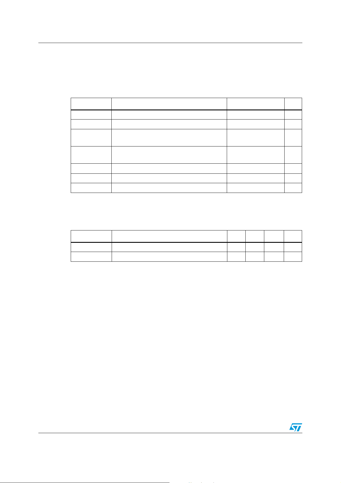
PM8903
VFQFPN16 3x3 mm
Description
The PM8903 is a high efficiency monolithic stepdown switching regulator designed to deliver up to
3 A continuous current. The IC operates from 2.8
V to 6 V input voltage (VIN).
The PM8903 features low-resistance integrated
nMOS and proprietary pulse-skipping mode for
optimum efficiency over all the loading range.
The voltage mode control loop allows the widest
range of output filter. Current sense is internally
thermally compensated for optimum precision.
The integrated 0.6 V reference allows the
regulation of output voltages with ±1% accuracy
over temperature variations. Switching frequency
is typically set to 1.1 MHz and can be
programmed to 0.8 MHz or 1.0 MHz. Out of phase
synchronization allows the reduction of input RMS
current.
The PM8903 provides precise dual-threshold
overcurrent protection as well as over /
undervoltage and overtemperature protection.
PGOOD output easily provides real-time
information on the output voltage.
The PM8903 is available in VFQFPN16 3 x 3 mm.
Table 1. Device summary
Order codes Package Packing
PM8903 VFQFPN16 3x3 mm Tube
PM8903TR VFQFPN16 3x3 mm Tape and reel
February 2012 Doc ID 022748 Rev 1 1/34
www.st.com
34
Page 2

Contents PM8903
Contents
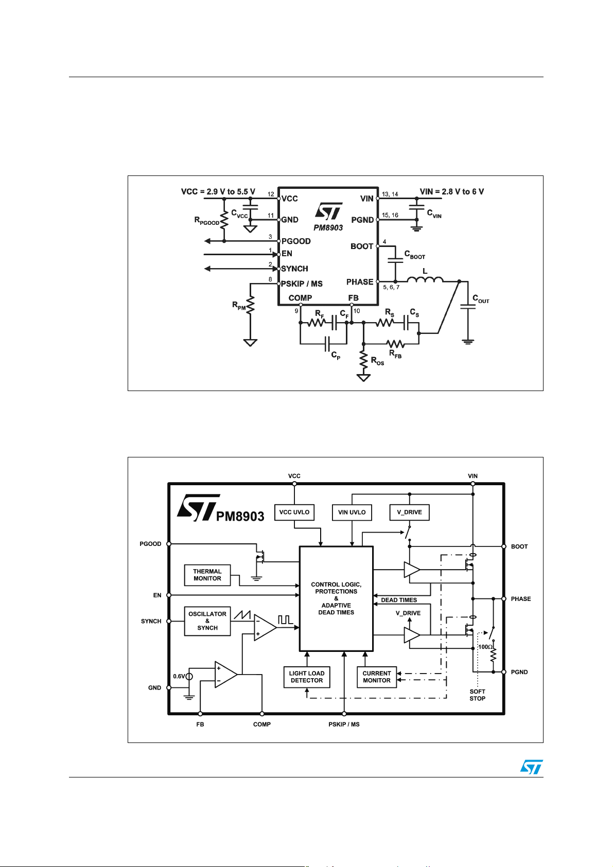
1 Typical application circuit and block diagram . . . . . . . . . . . . . . . . . . . . 3
1.1 Application circuit . . . . . . . . . . . . . . . . . . . . . . . . . . . . . . . . . . . . . . . . . . . . 3
1.2 Block diagram . . . . . . . . . . . . . . . . . . . . . . . . . . . . . . . . . . . . . . . . . . . . . . . 3
2 Pin description and connection diagrams . . . . . . . . . . . . . . . . . . . . . . . 4
2.1 Pin description . . . . . . . . . . . . . . . . . . . . . . . . . . . . . . . . . . . . . . . . . . . . . . 4
3 Thermal data . . . . . . . . . . . . . . . . . . . . . . . . . . . . . . . . . . . . . . . . . . . . . . . 6
4 Electrical specifications . . . . . . . . . . . . . . . . . . . . . . . . . . . . . . . . . . . . . . 7
4.1 Absolute maximum ratings . . . . . . . . . . . . . . . . . . . . . . . . . . . . . . . . . . . . . 7
4.2 Recommended operating conditions . . . . . . . . . . . . . . . . . . . . . . . . . . . . . 7
4.3 Electrical characteristics . . . . . . . . . . . . . . . . . . . . . . . . . . . . . . . . . . . . . . . 8
4.4 Typical operating characteristics . . . . . . . . . . . . . . . . . . . . . . . . . . . . . . . . 9
5 Device description . . . . . . . . . . . . . . . . . . . . . . . . . . . . . . . . . . . . . . . . . 11
5.1 Power section . . . . . . . . . . . . . . . . . . . . . . . . . . . . . . . . . . . . . . . . . . . . . . 11
5.2 Startup and shutdown management . . . . . . . . . . . . . . . . . . . . . . . . . . . . 12
5.2.1 Low-side-less startup . . . . . . . . . . . . . . . . . . . . . . . . . . . . . . . . . . . . . . . 13
5.2.2 Soft-off . . . . . . . . . . . . . . . . . . . . . . . . . . . . . . . . . . . . . . . . . . . . . . . . . . 13
5.3 Output voltage monitoring and protection . . . . . . . . . . . . . . . . . . . . . . . . 13
5.3.1 Overvoltage protection . . . . . . . . . . . . . . . . . . . . . . . . . . . . . . . . . . . . . . 13
5.3.2 Undervoltage protection . . . . . . . . . . . . . . . . . . . . . . . . . . . . . . . . . . . . . 14
5.3.3 Feedback disconnection protection . . . . . . . . . . . . . . . . . . . . . . . . . . . . 14
5.3.4 Power Good (PGOOD) . . . . . . . . . . . . . . . . . . . . . . . . . . . . . . . . . . . . . 14
5.4 Overcurrent protection . . . . . . . . . . . . . . . . . . . . . . . . . . . . . . . . . . . . . . . 15
5.5 Overtemperature protection . . . . . . . . . . . . . . . . . . . . . . . . . . . . . . . . . . . 15
5.6 Synchronization . . . . . . . . . . . . . . . . . . . . . . . . . . . . . . . . . . . . . . . . . . . . 15
5.7 Pulse-skipping . . . . . . . . . . . . . . . . . . . . . . . . . . . . . . . . . . . . . . . . . . . . . 16
5.8 Multifunction pin PSKIP/MS . . . . . . . . . . . . . . . . . . . . . . . . . . . . . . . . . . . 16
6 Application information . . . . . . . . . . . . . . . . . . . . . . . . . . . . . . . . . . . . . 17
6.1 Compensation network . . . . . . . . . . . . . . . . . . . . . . . . . . . . . . . . . . . . . . 17
2/34 Doc ID 022748 Rev 1
Page 3

PM8903 Contents
6.2 Output voltage setting . . . . . . . . . . . . . . . . . . . . . . . . . . . . . . . . . . . . . . . 19
6.3 Inductor design . . . . . . . . . . . . . . . . . . . . . . . . . . . . . . . . . . . . . . . . . . . . . 20
6.4 Output capacitors . . . . . . . . . . . . . . . . . . . . . . . . . . . . . . . . . . . . . . . . . . . 20
6.5 Input capacitors . . . . . . . . . . . . . . . . . . . . . . . . . . . . . . . . . . . . . . . . . . . . 21
7 PM8903 demonstration board . . . . . . . . . . . . . . . . . . . . . . . . . . . . . . . . 22
7.1 Detailed demonstration board description . . . . . . . . . . . . . . . . . . . . . . . . 23
7.1.1 Power input (VIN) . . . . . . . . . . . . . . . . . . . . . . . . . . . . . . . . . . . . . . . . . . 26
7.1.2 Signal input (VCC) . . . . . . . . . . . . . . . . . . . . . . . . . . . . . . . . . . . . . . . . . 27
7.1.3 Output (VOUT) . . . . . . . . . . . . . . . . . . . . . . . . . . . . . . . . . . . . . . . . . . . . 27
7.1.4 Test points and jumper connection . . . . . . . . . . . . . . . . . . . . . . . . . . . . 28
8 Package mechanical data . . . . . . . . . . . . . . . . . . . . . . . . . . . . . . . . . . . . 29
9 Revision history . . . . . . . . . . . . . . . . . . . . . . . . . . . . . . . . . . . . . . . . . . . 31
Doc ID 022748 Rev 1 3/34
Page 4
Typical application circuit and block diagram PM8903
1 Typical application circuit and block diagram
1.1 Application circuit
Figure 1. Typical application circuit
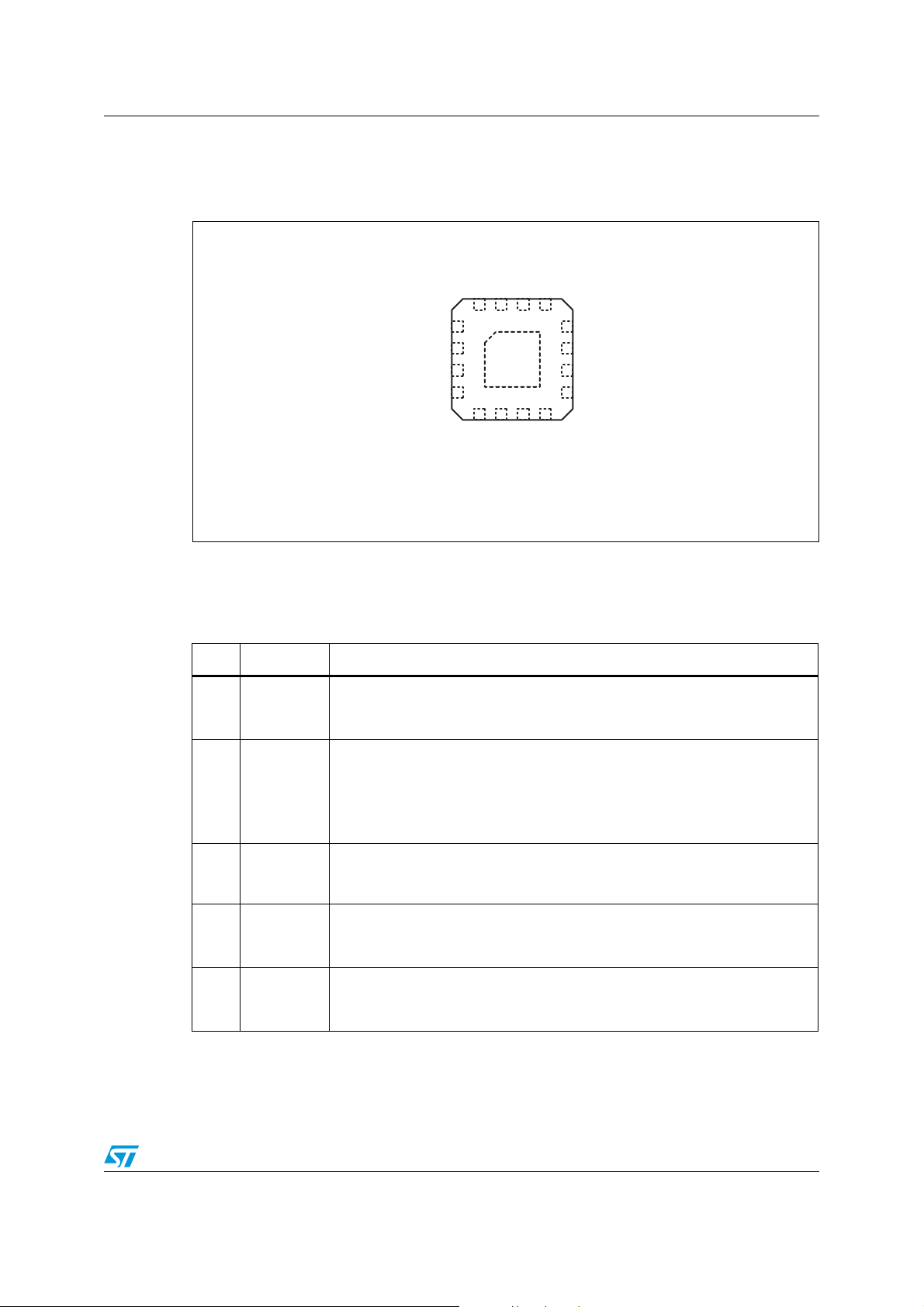
1.2 Block diagram
Figure 2. Block diagram
4/34 Doc ID 022748 Rev 1
Page 5
PM8903 Pin description and connection diagrams
2 Pin description and connection diagrams
Figure 3. Pin connection (top view)
PGND
PGND
VIN
VIN
16 15 14 13
EN
SYNCH
PGOOD
BOOT
1
2
3
4
5678
PHASE
PHASE
PHASE
12
11
10
9
PSKIP / MS
VCC
GND
FB
COMP
2.1 Pin description
Table 2. Pin description
Pin# Name Function
Enable. Internally pulled up by 5 μA to VCC.
1EN
2 SYNCH
3 PGOOD
4BOOT
5 to 7 PHASE
Force low to disable the device, set free or pull up above turn-on threshold to
enable the converter operations.
Synchronization pin.
According to PSKIP status, the IC sends the synchronization signal out of this
pin when master, while accepting a synchronization signal when slave.
Connect to the same SYNCH pin of a similar part when synchronizing ICs.
In case of single IC operation, leave floating.
Open drain output set free after SS has finished and pulled low when VOUT is
out of the PGOOD window or any protection is triggered.
Pull up to a voltage lower than VCC, if not used it can be left floating.
Bootstrap pin.
It provides power supply for the floating high-side driver. Connect with 0.1 μF
to PHASE. See
Output inductor connection.
The pins are connected to the embedded MOSFETs (high-side source and
low-side drain). Connect directly to output inductor. See
Figure 1
.
Figure 1
.
Doc ID 022748 Rev 1 5/34
Page 6

Pin description and connection diagrams PM8903
Table 2. Pin description (continued)
Pin# Name Function
Pulse-skip and master/slave definition.
Connect with a resistor to GND or leave it floating to define:
8 PSKIP / MS
9COMP
10 FB
11 GND
Pulse-skip feature status;
Master/slave for synchronization;
Switching frequency.
See
Section 5.8 on page 18
.
Error amplifier output.
Connect with an (R
- CF) // CP to FB. See
F
Figure 1
The device cannot be disabled by pulling low this pin.
Error amplifier inverting input.
Connect with R
COMP. A resistor R
or RFB // (RS - CS) to VSEN and with an (RF - CF) // CP to
FB
to GND sets the output voltage ratio. See
OS
Figure 1
All the internal references are referred to this pin. Connect to the PCB Signal
Ground.
12 VCC
13, 14 VIN
15, 16 PGND
Thermal pad
Device power supply.
Operative voltage is 2.9 V - 5.5 V. Filter with at least 1 μF MLCC vs. GND.
Power input voltage, connected to embedded high-side drain.
Supply range is from 2.8 V to 6 V. Bypass VIN pins to PGND pins close to the
IC package with high quality MLCC capacitors (at least 10 μF). See
Figure 1
Power ground connection, connected to embedded low-side MOSFET source.
Connect to PGND PCB plane. See
Figure 1
.
Thermal pad connects the silicon substrate and makes good thermal contact
with the PCB. Connect to the PCB PGND plane.
.
6/34 Doc ID 022748 Rev 1
Page 7

PM8903 Thermal data
3 Thermal data
Table 3. Thermal data
Symbol Parameter Value Unit
Thermal resistance junction to ambient
R
thJA
(Device soldered on standard demonstration board, see
Chapter 7 on page 24
for details)
30 °C/W
R
T
T
thJC
MAX
STG
T
J
Thermal resistance junction to case 12 °C/W
Maximum junction temperature 150 °C
Storage temperature range -40 to 150 °C
Junction temperature range -25 to 125 °C
Doc ID 022748 Rev 1 7/34
Page 8
Electrical specifications PM8903
4 Electrical specifications
4.1 Absolute maximum ratings
Table 4. Absolute maximum ratings
Symbol Parameter Value Unit
to PGND, GND -0.3 to 6 V
to PGND, GND -0.3 to 7 V
to PGND, GND
to PHASE
to PGND, GND
to PGND, GND, VIN=6 V, t<100 nsec.
to PGND, GND -0.3 to 7 V
to PGND, GND -0.3 to 6 V
EN
V
V
V
SYNCH
V
CC
V
IN
V
BOOT
PHASE
PGOOD
, V
All other pins to GND -0.3 to 3.6 V
4.2 Recommended operating conditions
Table 5. Recommended operating conditions
Symbol Parameter Min. Typ. Max. Unit
V
IN
V
CC
Power supply voltage 2.8 - 6 V
Signal supply voltage 2.9 - 5.5 V
-0.3 to 13
-0.3 to 6
-0.3 to 7
-1.7 to 7.5
V
V
8/34 Doc ID 022748 Rev 1
Page 9
PM8903 Electrical specifications
4.3 Electrical characteristics
VIN = V
= 3.3 V ± 5%, TJ = 0 °C to 125 °C, typical values at TJ = 25 °C, unless otherwise
CC
specified.
Table 6. Electrical characteristics
Symbol Parameter Test conditions Min. Typ. Max. Unit
Supply current and undervoltage lockout
I
I
CC
I
SHUTDOWN
VIN UVLO
VCC UVLO
Oscillator
F
SW
ΔV
OSC
d Duty cycle
T
ON-min
T
OFF-min
Reference and error amplifier
IN
VIN supply current Switching, no inductor connected 5 mA
VCC supply current Switching, no inductor connected 1 mA
VCC + VIN supply current Shutdown, EN = 0 V 7 μA
VIN turn-ON VIN rising 2.8 V
Hysteresis 100 mV
Deglitching
(1)
Rising and falling edge 1 μs
VCC turn-ON VCC rising 2.9 V
Hysteresis 100 mV
(1)
(1)
(1)
(1)
Rising and falling edge 1 μs
=0 Ω / 24 kΩ / 180 kΩ / 240 kΩ
R
PM
or PSKIP/MS pin floating
(1)
0.99 1.1 1.21 MHz
1V
0100%
80 ns
80 ns
Deglitching
Main oscillator accuracy
PWM ramp amplitude
Minimum ON time
Minimum OFF time
Output voltage accuracy VOUT = 0.6 V -1 - 1 %
A
0
DC gain
(1)
GBWP Gain-bandwidth product
SR Slew-rate
(1)
Output power MOSFETS
HS R
LS R
DS-on
DS-on
HS drain-source ON
resistance
LS drain-source ON
resistance
Overcurrent protection
I
OC1
I
OC2
1st level overcurrent
threshold
2nd level overcurrent
threshold
(1)
120 dB
(1)
C
=20 pF 5 V/μs
COMP
14 MHz
35 mΩ
35 mΩ
HS sourcing 4.0 4.6 5.2 A
HS sourcing 4.5 5.2 5.9 A
Doc ID 022748 Rev 1 9/34
Page 10
Electrical specifications PM8903
Table 6. Electrical characteristics (continued)
Symbol Parameter Test conditions Min. Typ. Max. Unit
Over and undervoltage protections
OVP OVP threshold
FB rising 0.69 0.72 0.75 V
LS turns off, FB falling 0.30 V
UVP UVP threshold FB falling 0.45 0.48 0.51 V
I
FB
FB disconnection bias
current
Sourced from FB 100 nA
Overtemperature protection
Thermal shutdown
threshold
(1)
140 °C
OTP
Thermal shutdown
hysteresis
(1)
40 °C
PGOOD
Upper threshold FB rising 0.69 0.72 0.75 V
PGOOD
Lower threshold FB falling 0.45 0.48 0.51 V
V
PGOODL
PGOOD voltage low I
= -4 mA 0.4 V
PGOOD
ENABLE
Input logic high EN rising 1.5 V
Input logic low EN falling 0.65 V
EN
Hysteresis 150 mV
Deglitching
(1)
Rising and falling edge 3 μs
SS
=0 Ω / 24 kΩ / 180 kΩ / 240 kΩ
R
T
SS
1. Guaranteed by design, not subject to test.
Soft-start time
PM
or PSKIP/MS pin floating
10/34 Doc ID 022748 Rev 1
0.79 ms
Page 11
PM8903 Electrical specifications
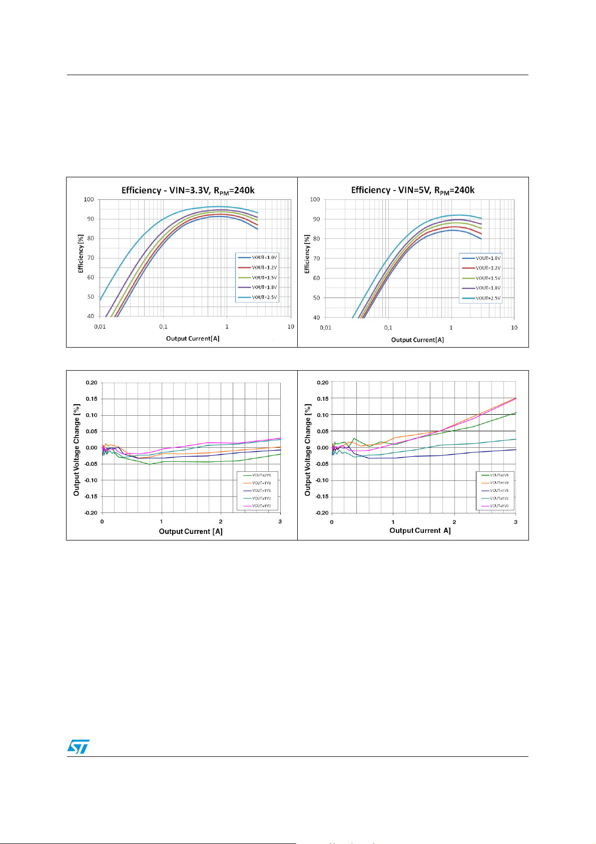
4.4 Typical operating characteristics
(The demonstration board as described in
V, VOUT=1V5, T
= 25 °C, unless otherwise specified.)
J
Figure 4. Efficiency vs. output current -
V
= 3.3 V
Figure 6. Load regulation - VIN = 3.3V Figure 7. Load regulation - V
IN
Chapter 7.1 on page 25
, R
=0 Ω, V
PM
Figure 5. Efficiency vs. output current -
V
= 5 V
IN
IN
IN
= 5 V
= V
CC
= 3.3
Doc ID 022748 Rev 1 11/34
Page 12

Electrical specifications PM8903
Figure 8. Line regulation - I
OUT
= 3 A
12/34 Doc ID 022748 Rev 1
Page 13

PM8903 Device description
5 Device description
The PM8903 is a high efficiency synchronous step-down monolithic switching regulator
capable of delivering up to 3 A continuous output current.
The power input voltage (V
) can range from 2.8 V to 6 V, the signal input voltage (VCC) can
IN
range from 2.9 V to 5.5 V.
Thanks to 0.6 V internal reference and 0-100% duty cycle capability, the PM8903 can
precisely regulate output voltages ranging from 0.6 V to almost V
T
time). The output voltage accuracy is better than ±1% over line, load and temperature.
OFF
The PM8903 embeds low R
(35 mΩ) N-channel MOSFETs for both HS (high-side) and
DS(on)
(limited only by minimum
IN
LS (low-side) and implements the proprietary pulse-skipping technology, therefore, the
PM8903 guarantees high efficiency over all the load range.
The voltage mode control loop with high bandwidth error amplifier and external
compensation enables a wide range of output filter configurations (including all MLCC
solutions) and fast response to load transient. The high-switching frequency (typically 1.1
MHz) and the small VFQFPN16 3x3 mm package allow very compact VR solutions.
The PM8903 features a full set of protections and output voltage monitoring:
● Precise and accurate dual level overcurrent protection (internally compensated against
temperature variations)
● Over and undervoltage protection
● Overtemperature protection
● Undervoltage lockout on both signal and power supply
● Power Good open drain output easily provides real-time information about the output
voltage
By simply connecting two PM8903s through the SYNCH pin, they can synchronize each
other with 180 ° phase shift switching interleaving, reducing RMS current absorption from
the input filter and preventing beating frequency noise, therefore allowing the size and cost
of the input filter to be reduced.
A simple resistor connected from the PSKIP / MS pin to ground enables / disables pulseskipping technology and assigns master or slave status to the IC.
The dedicated enable pin (EN) offers easy control on the power sequencing or to reset the
latched protection. Forcing the EN low, the device enters shutdown state and absorbs a total
quiescent current from VCC and VIN less than 15 μA.
5.1 Power section
The PM8903 integrates two low R
high-side switches, optimized for fast switching transition and high efficiency over all the load
range. The power stage is designed to deliver a continuous output current up to 3 A.
The HS MOSFET drain is connected to the VIN pins (power input), the LS MOSFET source
is connected to the PGND pins (power ground), HS MOSFET source and LS MOSFET drain
are connected together and to the PHASE pins (see
section is supplied from the VIN pins through an internal voltage regulator (V
assures the proper driving voltage over all the VIN range.
(35 mΩ) N-channel MOSFETs as low-side and
DS(on)
Figure 2 on page 4
Doc ID 022748 Rev 1 13/34
). The driving
) that
DRIVE
Page 14

Device description PM8903
To properly supply the power section the following is advised:
● Bypass VIN pins to PGND pins as close as possible to the IC package with high quality
MLCC capacitors (at least 10 μF).
● Connect the bootstrap capacitor (typically a 100 nF ceramic capacitor rated to stand
VIN voltage) from the BOOT pin to the PHASE pin to supply the HS driver.
Caution: Do not connect an external bootstrap diode.The IC already integrates an active bootstrap
diode to charge the bootstrap capacitor, saving the cost of this external component.
The PM8903 embodies an anti-shoot-through and adaptive dead-time control to minimize
low-side body diode conduction time and consequently reduce power losses:
● When the voltage at the PHASE pin drops (to check high-side MOSFET turn-off), the
LS MOSFET is suddenly switched on
● When the gate driving voltage of LS drops (to check low-side MOSFET turn-off), the
HS MOSFET is suddenly switched on.
If the current flowing in the inductor is negative, voltage on the PHASE pin never drops. A
watchdog controller is implemented to allow the LS MOSFET to turn on even in this case,
allowing the negative current of the inductor to recirculate. This mechanism allows the
system to regulate even if the current is negative (if pulse-skipping is disabled).
5.2 Startup and shutdown management
The PM8903 monitors the supply voltage on both VCC and VIN pins. Once both VCC and
VIN voltages are above the respective UVLO (under voltage lockout) thresholds and the EN
pin is high, the device waits for 0.5 ms (typ.) and then begins the soft-start.
Figure 9. PM8903 soft-start sequence
VIN
2.8V
2.7V
0.6V
VCC
EN
VREF
VIN UVLO
t
VCC UVLO
t
EN THRESHOLD 1.5V
t
t
T
=0.9 ms
0.5 ms
SS
14/34 Doc ID 022748 Rev 1
Page 15

PM8903 Device description
The PM8903 implements the soft-start by gradually increasing the internal reference from
0 V to 0.6 V in a 1024 switching clock (0.79 ms typ.), linearly charging the output capacitors
to the final regulation voltage in closed loop regulation. The soft-start prevents high inrush
current from power supply rail.
5.2.1 Low-side-less startup
In order to avoid any kind of negative undershoot and dangerous return from the load during
startup, the PM8903 performs a special sequence in enabling the LS driver to switch: during
the soft-start phase, the LS driver results disabled (LS = OFF) until the first PWM pulse
occurs. This avoids the dangerous negative spike on the output voltage that may happen if
starting over a pre-biased output.
As long as the output voltage is biased to a voltage higher than the programmed one, the
control loop does not provide the HS pulse that enables LS. In this case LS is enabled at the
end of the soft-start time and, if the device is allowed to sink (PSKIP disabled), it discharges
the output to the final regulation value.
This particular feature of the device masks the LS turn-on only from the control loop point of
view: protection has higher priority and can turn on the LS MOSFET if an overvoltage event
is detected.
5.2.2 Soft-off
The PM8903 implements the soft-off sequence turning off both HS and LS MOSFETs and
connecting the integrated bleeding resistor (100 Ω) between the PHASE and PGND pin.
When small load currents are applied to the converter, the soft-off sequence allows the
discharging of the output voltage within a maximum time (T
SO
output capacitance value.
T
SO
5 100 C
⋅⋅=
OUT
The PM8903 begins the soft-off sequence, and remains in a latched state, if one of the
following conditions occurs:
● VCC voltage falls below UVLO threshold
● OVP (overvoltage protection)
● UVP (undervoltage protection)
● OCP (overcurrent protection)
● EN pin is pulled low
Cycle EN or VCC to recover from latched state with a new soft-start sequence.
5.3 Output voltage monitoring and protection
The PM8903 monitors the output voltage status through the FB pin and compares the
voltage on this pin with the internal reference in order to provide over and undervoltage
protection as well as PGOOD signal.
) that depends only on the
5.3.1 Overvoltage protection
Overvoltage protection is active as soon as the device is enabled and both VCC and VIN
voltages are above the respective undervoltage lockout levels.
Doc ID 022748 Rev 1 15/34
Page 16

Device description PM8903
The protection is triggered when the voltage sensed on the FB pin rises over the OVP
threshold (0.72 V typ.) and the device acts as follows:
● HS MOSFET is suddenly forced OFF
● LS MOSFET is turned on (to discharge the output and protect the load) until V
to 0.3 V, then it is turned off (to avoid negative spikes on output voltage). If V
FB
drops
FB
recrosses OVP rising threshold, LS is turned on again
This protection state is latched, cycle EN or VCC to recover.
5.3.2 Undervoltage protection
Undervoltage protection is active from the end of soft-start.
If V
falls below the UVP threshold (0.48 V typ.), undervoltage protection is triggered and
FB
the device starts a soft-off sequence (see
Section 5.2.2
).
This protection state is latched, cycle EN, VCC or VIN to recover.
5.3.3 Feedback disconnection protection
In order to protect the load even if the FB pin is not connected to the PCB, a 100 nA current
is constantly sourced from the FB pin: if the FB pin is left floating, it is internally pulled high
triggering OVP protection and preventing V
from rising out of control.
OUT
Figure 10. FB disconnection
V
OUT
5.3.4 Power Good (PGOOD)
PGOOD is an open drain output, left floating when V
voltage, at the end of soft-start.
PGOOD is forced low, to communicate that the output voltage is no longer in regulation, if
one of the following conditions is verified:
● The voltage of the FB pin exits from the PGOOD window (±20% of V
● The device is disabled, EN is forced low
● VCC voltage is below the UVLO threshold
● Any protection is triggered (OVP, UVP, OCP, OTP)
R
FB
100nA
FB
R
OS
720mV
OVP
COMPARATOR
is in regulation at the programmed
OUT
)
REF
16/34 Doc ID 022748 Rev 1
Page 17

PM8903 Device description
5.4 Overcurrent protection
Overcurrent protection is active as soon as the device is enabled and both VCC and VIN
voltages are above the respective UVLO levels.
The overcurrent function protects the converter from a shorted output or overload by
sensing the output current information across the integrated MOSFETs as follows:
● During normal operation the output current information is monitored reading the current
flowing in the HS MOSFET
● When the converter is working with an ON time lower than 130 ns (typ.) the current is
monitored reading the current flowing in the LS MOSFET
If the monitored current information is bigger than the overcurrent thresholds, an overcurrent
event is detected.
For maximum safety and load protection, the PM8903 implements a dual level overcurrent
protection system.
● First level threshold
During a switching cycle, if the monitored current information exceeds a 4.6 A (typ.)
threshold, first level overcurrent is detected: the HS MOSFET is turned off and the LS
MOSFET is turned on until the next cycle. If four first level OC events are detected in
four consecutive switching cycles, overcurrent protection is triggered.
● Second level threshold
If the monitored current information exceeds the 5.2 A (typ.) threshold, overcurrent
protection is triggered immediately.
When overcurrent protection is triggered, the device suddenly turns off the HS and keeps
the LS turned on until the output current drops to 600 mA, then the device turns off both LS
and HS MOSFETs in a latched condition; cycle EN or VCC to recover.
5.5 Overtemperature protection
It is recommended that the device never exceeds the maximum allowable junction
temperature. This temperature increase is mainly caused by the total power dissipated from
the integrated power MOSFETs.
To avoid any damage to the device when reaching high temperature, the PM8903
implements a thermal shutdown feature: when the junction temperature reaches 140 °C the
device turns off both MOSFETs.
When the junction temperature drops to 100 °C, the device restarts with a new soft-start
sequence.
5.6 Synchronization
Synchronization of two PM8903s is enabled simply connecting the SYNCH pins of the two
devices together. No synchronization is implemented if the SYNCH pin is left floating.
When synchronization is enabled, the first device must be configured as a master and the
second device must be configured as a slave. Connect a resistor between the PSKIP/MS
pin and ground, and select the resistor value according to
master or slave.
Ta bl e 7
, to program the IC to be
Doc ID 022748 Rev 1 17/34
Page 18

Device description PM8903
Caution: Do not connect together the synchronization pin of two master devices in order to avoid any
damage to the ICs.
When two PM8903s are synchronized together they act as follows:
● Master mode
The SYNCH pin is configured as clock output. The device provides, on the SYNCH pin,
its internal switching clock information with a 180 ° time shifting.
● Slave mode
The SYNCH pin is configured as clock input. The device uses the clock information
received on the SYNCH pin to synchronize its internal switching clock.
5.7 Pulse-skipping
The PM8903 implements an ST proprietary adaptive pulse-skipping algorithm which
requires no configuration by the user and is independent from application setup and
parasites.
The algorithm allows to strongly increase the overall system efficiency skipping some
switching cycles (so reducing the equivalent switching frequency of the converter) when the
load current is low.
In many applications, MLCCs (multi layer ceramic capacitors) are used as the input or
output filter, or both. MLCCs can produce audible noise if the switching frequency is in the
human hearing range. To avoid audible noise, the PM8903 pulse-skipping algorithm limits
the minimum equivalent switching frequency above the audio band.
Pulse-skipping mode is enabled connecting a resistor between the PSKIP/MS pin and
ground, and selects the resistor value according to
5.8 Multifunction pin PSKIP/MS
With this pin it is possible to:
● enable/disable the pulse-skipping management
● assign to the IC master or slave status
● select the switching frequency
Connect a resistor (R
functionality according to
Table 7. PSKIP/MS pin configuration
R
PM
0 Ω Disabled Slave 1.1 MHz
24 kΩ Enabled Slave 1.1 MHz
56 kΩ Disabled Slave 0.8 MHz
110 kΩ Disabled Master 1.0 MHz
180 kΩ Enabled Master 1.1 MHz
) between the PSKIP/MS pin and GND in order to set the IC
PM
Ta bl e 7
.
Pulse-skipping Synch mode Switching frequency
Ta b le 7
.
240 kΩ
(or pin floating)
18/34 Doc ID 022748 Rev 1
Disabled Master 1.1 MHz
Page 19

PM8903 Application information
6 Application information
6.1 Compensation network
The PM8903 implements a voltage mode control loop (see
Figure 11
). The output voltage is
regulated to the internal reference (offset resistor between FB node and GND can be
neglected in control loop calculation).
Error amplifier output is compared with the oscillator sawtooth waveform to provide the
PWM signal to the driver section. The PWM signal is then transferred to the switching node
with V
amplitude. This waveform is filtered by the output filter.
IN
The converter transfer function is the small signal transfer function between the output of the
EA and V
filter and a zero at F
modulator is simply the input voltage V
ΔV
OSC
. This function has a double pole at frequency FLC depending on the L-C output
OUT
depending on the output capacitor ESR. The DC gain of the
ESR
divided by the peak-to-peak oscillator voltage
IN
.
Figure 11. PM8903 control loop
Modulator
ΔV
OSC
DRIVER
OSC
DRIVER
HS
LS
V
IN
PHASE
L
DCR
Output Filter
ESR
C
OUT
V
OUT
V
REF
ERROR
AMPLIFIER
FB
COMP
R
C
F
F
C
P
Z
F
R
OS
The compensation network closes the loop joining V
function ideally equal to -Z
F/ZFB
.
R
FB
C
R
S
S
Z
FB
and EA output with a transfer
OUT
The compensation goal is to close the control loop assuring high DC regulation accuracy,
good dynamic performance, and stability. To achieve this, the overall loop needs high DC
gain, high bandwidth and good phase margin.
High DC gain is achieved giving an integrator shape to the compensation network transfer
function. Loop bandwidth (F
) can be fixed choosing the right RF/RFB ratio, however, for
0dB
Doc ID 022748 Rev 1 19/34
Page 20

Application information PM8903
stability, it should not exceed FSW/2π. To achieve a good phase margin, the control loop gain
must cross the 0 dB axis with -20 dB/decade slope.
As an example,
Figure 12
shows an asymptotic bode plot of a type III compensation.
Figure 12. Example of type III compensation
The open loop converter singularities are:
F
F
LC
ESR
1
------------- ------------- --------=
⋅
2π LC
------------- ------------- ------------ ----- -=
2π C
OUT
OUT
1
ESR⋅⋅
The compensation network singularity frequencies are:
F
Z1
F
Z2
F
P1
F
P2
20/34 Doc ID 022748 Rev 1
1
------------- ------------- ----=
⋅⋅
2π R
FCF
------------- ------------- ------------ ------------- --=
2π R
------------ ------------- ------------- ------------=
2π R
------------- ------------- -----=
2π R
1
+()C
⋅⋅
FBRS
S
1
CFCP⋅
⎛⎞
------------- --------
⋅⋅
F
⎝⎠
C
+
FCP
1
⋅⋅
SCS
Page 21

PM8903 Application information
The following suggestions may be followed in order to place the poles and zeroes of the
compensation network.
● Select a value for R
● Select R
in order to obtain the desired closed loop regulator bandwidth according to
F
in the range of some kΩ
FB
the approximate formula:
F
ΔV
R
F
● Select C
C
F
0dB
------------
F
LC
in order to place FZ1 below FLC (typically 0.1*FLC):
F
------------- ------------- ------------ --------=
2π R
OSC
--------------------- -
⋅⋅=
V
IN_MAX
1
0.1 F
⋅⋅ ⋅
F
LC
R
FB
● Select C
C
● Select C
in order to place FP1 at 0.5*FSW:
P
1
------------ ------------- ------=
P
π R
⋅⋅
FFSW
and RS in order to place FZ2 at FLC and FP2 at half of the switching
S
frequency:
------------- ------------- -----------=
⋅⋅
2π R
FBFLC
1
------------ ------------- ------=
π C
⋅⋅
SFSW
1
C
S
R
S
● Check that compensation network gain is lower than open loop EA gain before F
Check phase margin obtained (it should be greater than 45 °)
●
● Repeat the whole procedure if necessary.
6.2 Output voltage setting
The PM8903 integrates a 0.6 V internal reference (V
line, load, and temperature variations (excluding external resistor divider tolerance, when
present).
The output voltage can be easily programmed connecting ROS and RFB resistors as follows
(see also
● Connect pin FB to V
● Connect pin FB to GND through R
Usually, the R
bandwidth (see
voltage.
Figure 1 on page 4
resistor is selected in order to obtain the desired closed loop regulator
FB
Section 6.1
).
through RFB resistor
OUT
for details) and it is not changed when setting the output
resistor
OS
), with a total accuracy of ±1% over
REF
0dB
Therefore, the output voltage setting is easily achieved using the following formula to select
the value of the R
R
OS
R
resistor:
OS
------------- ------------- -------- -
⋅=
FB
V
OUTVREF
V
REF
–
Doc ID 022748 Rev 1 21/34
Page 22

Application information PM8903
6.3 Inductor design
The inductance value is defined by a compromise between the dynamic response time, the
efficiency, the cost, and the size. The inductor must be calculated to maintain the ripple
current (ΔI
value can be calculated with the following relationship:
L
) between 20% and 30% of the maximum output current (typ.). The inductance
L
V
–
INVOUT
------------ ------------- ---- -
F
SWΔIL
V
OUT
--------------
⋅=
⋅
V
IN
where F
is the switching frequency, VIN is the input voltage, and V
SW
voltage.
Increasing the value of the inductance reduces the current ripple but, at the same time,
increases the converter response time to a dynamic load change. The response time is the
time required by the inductor to change its current from the initial to the final value. Until the
inductor finishes its charging time, the output current is supplied by the output capacitors.
Minimizing the response time can minimize the output capacitance required. If the
compensation network is well designed, during a load variation the device is able to set a
duty cycle value very different (0% or 100%) from the steady-state one. When this condition
is reached, the response time is limited by the time required to change the inductor current.
6.4 Output capacitors
The output capacitors are basic components to define the ripple voltage across the output
and for the fast transient response of the power supply. They depend on the output voltage
ripple requirements, as well as any output voltage deviation requirement during a load
transient.
During steady-state conditions, the output voltage ripple is influenced by both the ESR and
the capacitive value of the output capacitors as follows:
ΔV
ΔV
OUT_ESR
OUT_C
ΔILESR⋅=
------------ ------------- ------------ - -
ΔI
⋅=
L
⋅⋅
8C
1
OUTFSW
is the output
OUT
where ΔI
is the inductor current ripple. In particular, the expression that defines ΔV
L
takes into consideration the output capacitor charge and discharge as a consequence of the
inductor current ripple.
During a load variation, the output capacitor supplies the current to the load or absorbs the
current stored in the inductor until the converter reacts. In fact, even if the controller
recognizes immediately the load transient and sets the duty cycle at 100% or 0%, the
current slope is limited by the inductor value. The output voltage has a drop that also in this
case depends on the ESR and capacitive charge/discharge as follows:
ΔV
OUT_ESR
ΔV
OUT_C
where ΔV
( for the load appliance or V
D
MAXVINVOUT
is the voltage applied to the inductor during the transient response
L
–⋅
ΔI
ΔI
OUT
------------ ------------- -------------
⋅=
OUT
2C
ESR⋅=
L ΔI
⋅
OUT
⋅⋅
OUTΔVL
OUT
MLCC capacitors have typically low ESR to minimize the ripple but also have low
capacitance that does not minimize the voltage deviation during dynamic load variations.
22/34 Doc ID 022748 Rev 1
for the load removal).
OUT_C
Page 23

PM8903 Application information
Electrolytic capacitors have a large capacitance to minimize voltage deviation during load
transients while they do not show the same ESR values as the MLCC resulting then in
higher ripple voltages.
A mix between an electrolytic and MLCC capacitor can be used to minimize ripple as well as
reducing voltage deviation in dynamic mode.
The high bandwidth error amplifier of PM8903 and external compensation enables a wide
range of output filter configurations (including all MLCC solutions) and fast transient
response.
6.5 Input capacitors
The input capacitor bank is designed considering mainly the input RMS current that
depends on the output deliverable current (I
follows:
) and the duty-cycle (D) for the regulation as
OUT
I
rmsIOUT
The equation reaches its maximum value, I
D1D–()⋅⋅=
OUT
input capacitor ESR and, in the worst case, are:
PESRI
⋅=
OUT
2
2⁄()
/2, with D = 0.5. The losses depend on the
Doc ID 022748 Rev 1 23/34
Page 24

PM8903 demonstration board PM8903
7 PM8903 demonstration board
The PM8903 demonstration board realizes, in a four-layer PCB, a high efficiency
synchronous step-down monolithic switching converter capable of delivering up to 3 A
continuous output current.
The demonstration board shows the operation of the device in a general purpose
application. Two devices are present on the demonstration board and connected through the
SYNCH pin, also allowing testing of the synchronization capability of the PM8903. The two
devices are synchronized to each other with 180 ° phase shift switching interleaving,
reducing RMS current absorption from the input filter and preventing beating frequency
noise, therefore allowing a reduction in the size and cost of input filter.
Figure 13. PM8903 demonstration board
The input voltage (VIN) can range from 2.8 V to 6 V and the supply voltage (VCC) can range
from 2.9 V to 5.5 V.
The output voltage is programmed to be 1.5 V but can be easily programmed, changing a
single resistor, from 0.6 V to almost V
and temperature.
A simple resistor connected from the PSKIP / MS pin to ground enables / disables pulseskipping technology and assigns to the IC master or slave status.
The dedicated dip switch SW1 allows the enabling / disabling of each device and offers easy
control on the power sequencing or to reset latched protection. Forcing EN low, the device
enters a shutdown state and absorbs a total quiescent current from VCC and VIN less than
15 μA.
24/34 Doc ID 022748 Rev 1
with a total accuracy better than ±1% over line, load
IN
Page 25

PM8903 PM8903 demonstration board
7.1 Detailed demonstration board description
This section describes:
● demonstration board schematics, see
● demonstration board layout, see
● demonstration board BOM (bill of materials), see
Moreover, the following subsection details how to configure and use the standard
demonstration board.
Figure 14
Figure 15
Ta bl e 8
Doc ID 022748 Rev 1 25/34
Page 26

PM8903 demonstration board PM8903
Figure 14. PM8903 demonstration board schematic
JP
1
JP
2
C6, C8, C
MARGIN1
VIN1
VIN2
9
R
6
C
5
R14R
C15C
R
8
C
10
R
15
VIN
11
16
VOUT1
L
1
R
13
R
17
VCC
C
11
R
1
R
VIN1
D
1
C2, C
2
13, 14
C
4
3
VIN
VCC1
12
VCC
11
GND
C
1
BOOT
4
PM8903
15, 16, EP
R
1
2
3
8
10
PGND
EN
SYNCH
PGOOD
PSKIP/MS
COMP
9
5, 6, 7
PHASE
FB
C
12
10
R12C
13
C
14
R
16
R
R
4
R
3
5
EN1
Q
1
R
R9C
7
7
R
18
EN1 EN2
SW
1
VIN
PM8903
PGND
EN
SYNCH
PGOOD
PSKIP/MS
COMP
9
VCC2
12
VCC
C
ON ON
C
17
11
GND
BOOT
PHASE
4
5, 6, 7
R
6
C
5
R
C
FB
C
27
10
R30C
28
29
R32R
R
34
1 2
VOUT2
L
2
C22, C23, C
26
26
R
29
33
R
31
R
35
24
MARGIN2
R
19
R
19
20
13, 14
C
20
15, 16, EP
VIN2
D
2
R
R
21
22
C18, C
R
23
EN2
1
2
Q
2
R
R27 C
25
25
3
8
R
28
26/34 Doc ID 022748 Rev 1
Page 27

PM8903 PM8903 demonstration board
Figure 15. PM8903 demonstration board layout
TOP LAYER INNER-1 LAYER
INNER-2 LAYER BOTTOM LAYER
Table 8. PM8903 demonstration board - bill of material
Reference Alias Value Manufacturer P.N. Package Supplier
Resistors
R1, R7, R9, R19,
R25, R27
NM 0603
R2, R20 10 Ω 0603
R3, R21 R
PGOOD(1,2)
10 kΩ 0603
R4, R22 1 kΩ 0603
R5, R23 560 kΩ 0603
R6, R24 R
R8, R26 R
R10 R
R11, R29 R
R12, R30 R
R13, R17, R18,
R31, R35
R14, R32 R
BOOT(1,2)
SNUBBER(1,2)
PM(1)
S(1,2)
F(1,2)
FB1(1,2)
0 Ω 0603
NM 0603
270 kΩ 0603
100 Ω 0603
680 Ω 0603
0 Ω 0603
0 Ω 0603
Doc ID 022748 Rev 1 27/34
Page 28

PM8903 demonstration board PM8903
Table 8. PM8903 demonstration board - bill of material (continued)
Reference Alias Value Manufacturer P.N. Package Supplier
R15, R33 R
R16, R34 R
R28 R
FB2(1,2)
OS(1,2)
PM(2)
3.3 kΩ 0603
2.2 kΩ 0603
0 Ω 0603
Capacitors
C1, C17 C
C2, C3, C18, C19 C
C4, C20 C
C5, C21 C
C6, C8, C9, C22,
C23, C24
C
VCC(1,2)
VIN(1,2)
VIN(1,2)
BOOT(1,2)
OUT(1,2)
10 µF X7R 6.3 V 10% - MLCC GRM21BR70J106KE 0805 MURATA
1 µF, X7R 0603
22 µF, X5R, 6.3 V, 10% -
MLCC
GRM21BR60J226ME 0805 MURATA
100 nF, X7R 0603
100 nF, X7R 0603
C7, C25 NM 0603
C10, C26 C
SNUBBER(1,2)
C11 C
C12, C27 C
C13, C28 C
C14, C29 C
C15a, C16 C
C15 C
VCC
S(1,2)
F(1,2)
P(1,2)
IN
IN)
10 µF X7R 6.3 V 10% - MLCC GRM21BR70J106KE 0805 MURATA
NM 0603
4.7 nF, X7R 0603
22 nF, X7R 0603
220 pF, X7R 0603
NM Case D
NM T.H.M
Inductors
L1, L2 1.0 µH, 10.4 mΩ SPM5030T-1R0M TDK
Alternative inductors
1.2 µH, 35 mΩ H.DI0520-1R2 NEC
L1, L2
1.2 µH, 25 mΩ LTF5022T-1R2N4R2-LC TDK
Active components
D1, D2 LED
Q1, Q2 2N7002 STM
U1, U2 PM8903 STM
7.1.1 Power input (VIN)
Connect a power supply to connectors J4(VIN) and J5(GND) on the demonstration board to
provide voltage on the power input pins of both devices. Input voltage can range from 2.8 V
to 6 V bus.
28/34 Doc ID 022748 Rev 1
Page 29

PM8903 PM8903 demonstration board
If the voltage is between 2.9 V and 5.5 V it can supply also the signal input pins of both
devices (through the V
pin). In this case, make sure that resistors R2/R20 are NM (not
CC
mounted) and mount 0 Ω resistors on R1/R19 locations.
7.1.2 Signal input (VCC)
The controller is usually supplied separately from the power stage through the VCC input
pins.
Connect a power supply to connector J2 (pin one is VC and pin two is GND) on the
demonstration board to provide voltage on the signal input pins of both devices. Supply
voltage can range from 2.9 V to 5.5 V.
7.1.3 Output (V
On the standard demonstration board, the output voltage is programmed to be 1.5 V, but it
can be easily changed mounting one of the values suggested in
Select the R
custom value for the output voltage of each device.
R
where:
● V
● V
● R
Table 9. Typical R
R
OS
FB
is the desiderated output voltage
OUT
is the internal voltage reference (0.6 V)
REF
resistor, on the demonstration board, is the sum of two resistors (R14/R15 for
FB
device U1 and R32/R33 for device U2) and have a total value of 3.3 kΩ
Programmed output voltage Resistor value
)
OUT
Ta bl e 9
(R16/R34) resistor value with the following formula in order to program a
OS
V
REF
------------- ------------- -------- -
⋅=
V
–
OUTVREF
resistors (R16/R34)
OS
0.6 V NM
0.8 V 10 kΩ
1.0 V 4.9 kΩ
1.2 V 3.3 kΩ
1.5 V 2.2 kΩ
.
1.8 V 1.65 kΩ
2.5 V 1 kΩ
Doc ID 022748 Rev 1 29/34
Page 30

PM8903 demonstration board PM8903
7.1.4 Test points and jumper connection
Use the following test points in order to measure the most important signals of the PM8903.
● VCC1 / VCC2: monitor the supply voltages
● VIN1 / VIN2: monitor the input voltages
● V_OUT_S1 / V_OUT_S2: monitor the output voltages (use these test points to perform
efficiency load-line regulation measurements)
● PGOOD1 / PGOOD2: (active high) monitor the regular functioning of the controllers
● SYNCH1 / SYNCH2: these are usually shorted when two devices are synchronized
together
Unplug jumpers JP1 /JP2 in order to remove the power input voltage from device U1, device
U2, or both. Provide power supply voltage to one device at a time when performing
efficiency tests.
Turn on Dip-Switch SW1 in order to disable device U1, device U2, or both.
30/34 Doc ID 022748 Rev 1
Page 31

PM8903 Package mechanical data
8 Package mechanical data
In order to meet environmental requirements, ST offers these devices in different grades of
®
ECOPACK
packages, depending on their level of environmental compliance. ECOPACK
specifications, grade definitions and product status are available at: www.st.com. ECOPACK
is an ST trademark.
Table 10. VFQFPN16 3 x 3 x 1.0 mm mechanical data
mm
Dim.
Min. Typ. Max.
A 0.80 0.90 1.00
A1 0.02 0.05
A2 0.65 1.00
A3 0.20
b 0.18 0.25 0.30
D 2.85 3.00 3.15
D1 1.50
D2 1.60
E 2.85 3.00 3.15
E1 1.50
E2 1.60
e 0.45 0.50 0.55
L 0.30 0.40 0.50
ddd 0.08
Doc ID 022748 Rev 1 31/34
Page 32

Package mechanical data PM8903
Figure 16. Package dimensions
32/34 Doc ID 022748 Rev 1
Page 33

PM8903 Revision history
9 Revision history
Table 11. Document revision history
Date Revision Changes
01-Feb-2012 1 First release
Doc ID 022748 Rev 1 33/34
Page 34

PM8903
Please Read Carefully:
Information in this document is provided solely in connection with ST products. STMicroelectronics NV and its subsidiaries (“ST”) reserve the
right to make changes, corrections, modifications or improvements, to this document, and the products and services described herein at any
time, without notice.
All ST products are sold pursuant to ST’s terms and conditions of sale.
Purchasers are solely responsible for the choice, selection and use of the ST products and services described herein, and ST assumes no
liability whatsoever relating to the choice, selection or use of the ST products and services described herein.
No license, express or implied, by estoppel or otherwise, to any intellectual property rights is granted under this document. If any part of this
document refers to any third party products or services it shall not be deemed a license grant by ST for the use of such third party products
or services, or any intellectual property contained therein or considered as a warranty covering the use in any manner whatsoever of such
third party products or services or any intellectual property contained therein.
UNLESS OTHERWISE SET FORTH IN ST’S TERMS AND CONDITIONS OF SALE ST DISCLAIMS ANY EXPRESS OR IMPLIED
WARRANTY WITH RESPECT TO THE USE AND/OR SALE OF ST PRODUCTS INCLUDING WITHOUT LIMITATION IMPLIED
WARRANTIES OF MERCHANTABILITY, FITNESS FOR A PARTICULAR PURPOSE (AND THEIR EQUIVALENTS UNDER THE LAWS
OF ANY JURISDICTION), OR INFRINGEMENT OF ANY PATENT, COPYRIGHT OR OTHER INTELLECTUAL PROPERTY RIGHT.
UNLESS EXPRESSLY APPROVED IN WRITING BY TWO AUTHORIZED ST REPRESENTATIVES, ST PRODUCTS ARE NOT
RECOMMENDED, AUTHORIZED OR WARRANTED FOR USE IN MILITARY, AIR CRAFT, SPACE, LIFE SAVING, OR LIFE SUSTAINING
APPLICATIONS, NOR IN PRODUCTS OR SYSTEMS WHERE FAILURE OR MALFUNCTION MAY RESULT IN PERSONAL INJURY,
DEATH, OR SEVERE PROPERTY OR ENVIRONMENTAL DAMAGE. ST PRODUCTS WHICH ARE NOT SPECIFIED AS "AUTOMOTIVE
GRADE" MAY ONLY BE USED IN AUTOMOTIVE APPLICATIONS AT USER’S OWN RISK.
Resale of ST products with provisions different from the statements and/or technical features set forth in this document shall immediately void
any warranty granted by ST for the ST product or service described herein and shall not create or extend in any manner whatsoever, any
liability of ST.
ST and the ST logo are trademarks or registered trademarks of ST in various countries.
Information in this document supersedes and replaces all information previously supplied.
The ST logo is a registered trademark of STMicroelectronics. All other names are the property of their respective owners.
© 2012 STMicroelectronics - All rights reserved
STMicroelectronics group of companies
Australia - Belgium - Brazil - Canada - China - Czech Republic - Finland - France - Germany - Hong Kong - India - Israel - Italy - Japan -
Malaysia - Malta - Morocco - Philippines - Singapore - Spain - Sweden - Switzerland - United Kingdom - United States of America
www.st.com
34/34 Doc ID 022748 Rev 1
 Loading...