

Integrated IEEE 802.3af compliant PoE-PD interface
and PWM controller with support of external source
Features
■ IEEE 802.3af compliant PD interface
■ Works with power supplied from Ethernet LAN
cables or from local auxiliary sources
■ Integrated 100 V, 0.5 Ω, 800 mA hot-swap
MOSFET
■ Integrated signature resistor
■ Programmable in-rush current limit
■ Programmable classification current
■ Programmable DC current limit up to 800 mA
■ High voltage start-up bias regulator
■ Thermal shutdown protection
■ Current mode pulse width modulator
■ Programmable oscillator frequency
■ Programmable soft-start
■ Power good indication
■ 80 % maximum duty cycle with internal slope
compensation
■ Supports both isolated and non-isolated
Applications.
■ HTSSOP16 package
Applications
■ VoIP phones, WLAN access points
■ Security cameras
■ PoE powered device appliances
■ High power (>12.95 W) powered devices
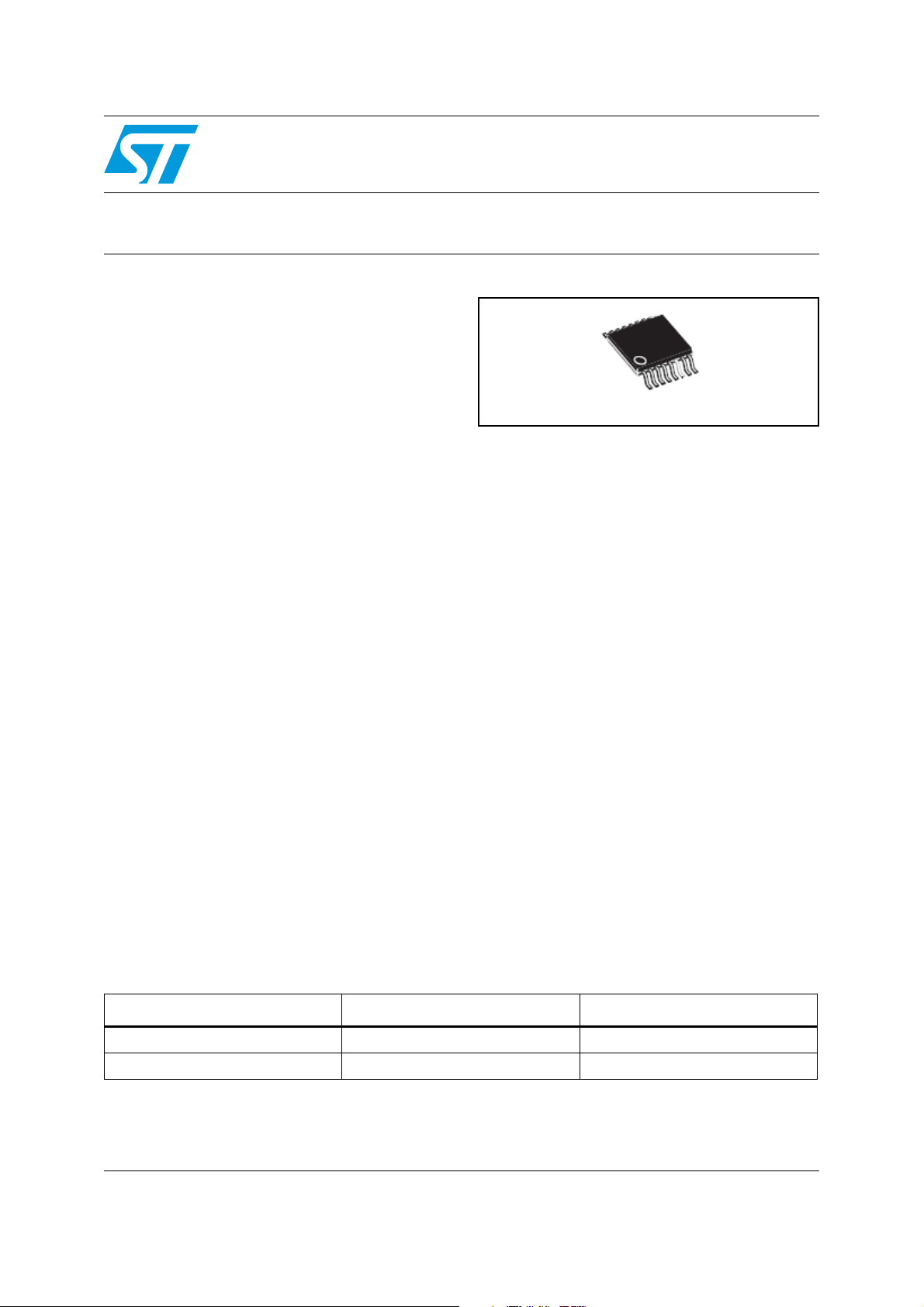
PM8800A
HTSSOP16
Description
The PM8800A integrates a standard power over
Ethernet (PoE) interface and a current mode
PWM controller to simplify the design of the
power supply sections of all powered devices.
The PoE interface incorporates all the functions
required by the IEEE 802.3af including detection,
classification, under-voltage lockout (UVLO) and
in-rush current limitation.
PM8800A specifically targets PD with extended
power requirement with respect to the limit
imposed by the 802.3af standard, embedding a
hot-swap MOSFET capable of sustaining twice
the current of the 802.3af standard with a
programmable DC current limit.
The integrated switching regulator has been
designed to work with power either form the
Ethernet cable connection or from an external
power source such as AC adapter.
The DC-DC section of the PM8800A features a
programmable oscillator frequency, soft-start,
slope compensation and embeds a voltage output
error amplifier allowing use in both isolated and
non isolated configuration.
Table 1. Device summary
Order codes Package Packing
PM8800A HTSSOP16 Tube
PM8800ATR HTSSOP16 Tape and reel
February 2008 Rev 2 1/35
www.st.com
35

Contents PM8800A
Contents
1 Typical application circuit and block diagram . . . . . . . . . . . . . . . . . . . . 4
1.1 Application circuits . . . . . . . . . . . . . . . . . . . . . . . . . . . . . . . . . . . . . . . . . . . 4
1.2 Block diagram . . . . . . . . . . . . . . . . . . . . . . . . . . . . . . . . . . . . . . . . . . . . . . . 5
2 Pins description and connection diagrams . . . . . . . . . . . . . . . . . . . . . . 6
2.1 Pin descriptions . . . . . . . . . . . . . . . . . . . . . . . . . . . . . . . . . . . . . . . . . . . . . 6
2.2 Thermal data . . . . . . . . . . . . . . . . . . . . . . . . . . . . . . . . . . . . . . . . . . . . . . . 8
3 Electrical specifications . . . . . . . . . . . . . . . . . . . . . . . . . . . . . . . . . . . . . . 9
3.1 Absolute maximum ratings . . . . . . . . . . . . . . . . . . . . . . . . . . . . . . . . . . . . . 9
3.2 Electrical characteristic . . . . . . . . . . . . . . . . . . . . . . . . . . . . . . . . . . . . . . 10
4 Device description and operation . . . . . . . . . . . . . . . . . . . . . . . . . . . . . 14
5 PD interface . . . . . . . . . . . . . . . . . . . . . . . . . . . . . . . . . . . . . . . . . . . . . . . 16
5.1 Detection . . . . . . . . . . . . . . . . . . . . . . . . . . . . . . . . . . . . . . . . . . . . . . . . . 16
5.2 Classification . . . . . . . . . . . . . . . . . . . . . . . . . . . . . . . . . . . . . . . . . . . . . . 17
5.3 Under voltage lock-out . . . . . . . . . . . . . . . . . . . . . . . . . . . . . . . . . . . . . . . 18
5.4 In rush current limit . . . . . . . . . . . . . . . . . . . . . . . . . . . . . . . . . . . . . . . . . . 18
5.5 Continuos current limitation . . . . . . . . . . . . . . . . . . . . . . . . . . . . . . . . . . . 20
5.6 HV regulator startup . . . . . . . . . . . . . . . . . . . . . . . . . . . . . . . . . . . . . . . . . 21
5.7 Power good indication . . . . . . . . . . . . . . . . . . . . . . . . . . . . . . . . . . . . . . . 22
6 PWM section . . . . . . . . . . . . . . . . . . . . . . . . . . . . . . . . . . . . . . . . . . . . . . 23
6.1 Error amplifier and loop compensation . . . . . . . . . . . . . . . . . . . . . . . . . . . 23
6.2 Oscillator and sync capability . . . . . . . . . . . . . . . . . . . . . . . . . . . . . . . . . . 24
6.3 Soft start . . . . . . . . . . . . . . . . . . . . . . . . . . . . . . . . . . . . . . . . . . . . . . . . . . 25
6.4 PWM comparator / slope compensation . . . . . . . . . . . . . . . . . . . . . . . . . 26
6.5 Current limiting . . . . . . . . . . . . . . . . . . . . . . . . . . . . . . . . . . . . . . . . . . . . . 26
6.6 Leading edge blanking . . . . . . . . . . . . . . . . . . . . . . . . . . . . . . . . . . . . . . . 28
6.7 Thermal protection . . . . . . . . . . . . . . . . . . . . . . . . . . . . . . . . . . . . . . . . . . 28
2/35

PM8800A Contents
7 Auxiliary sources . . . . . . . . . . . . . . . . . . . . . . . . . . . . . . . . . . . . . . . . . . 29
8 Package mechanical data . . . . . . . . . . . . . . . . . . . . . . . . . . . . . . . . . . . . 32
8.1 HTSSOP16 mechanical data . . . . . . . . . . . . . . . . . . . . . . . . . . . . . . . . . . 33
9 Revision history . . . . . . . . . . . . . . . . . . . . . . . . . . . . . . . . . . . . . . . . . . . 34
3/35
Typical application circuit and block diagram PM8800A
1 Typical application circuit and block diagram
1.1 Application circuits
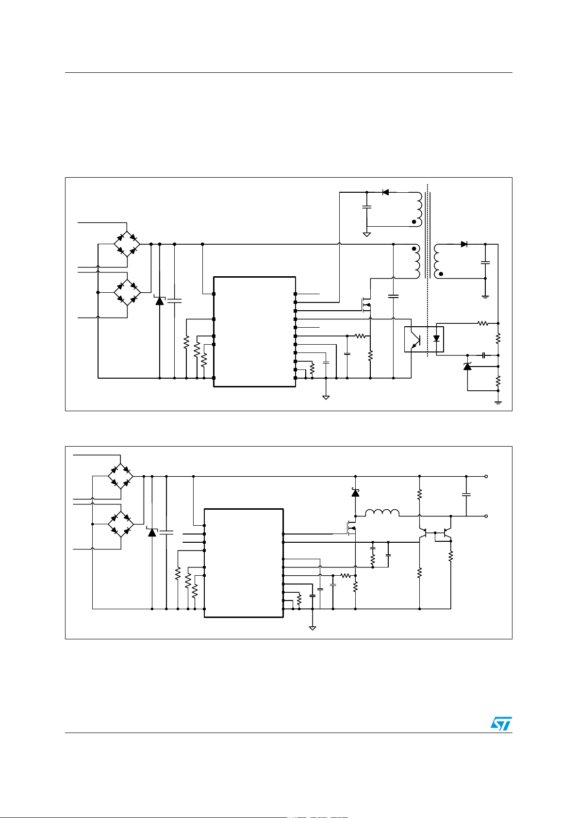
Figure 1. Simplified application schematic for powered devicesing PM8800A in isolated
configuration
VIN
AUXI_IRL
DCCL
RCLASS
VSS
PM8800
A
AUXII
VCC
GD
COMP
nPGD
CS
VFB
SS
RT
GND
AGND
Figure 2. Simplified application schematic for powered device using PM8800A in non-isolated
buck configuration
Vin
VIN
AUXII
nPGD
AUXI_IRL
DCCL
RCLASS
VSS
PM8800
A
GD
VFB
VCC
COMP
CS
SS
RT
GND
AGND
Vout+
Vout-
4/35
PM8800A Typical application circuit and block diagram
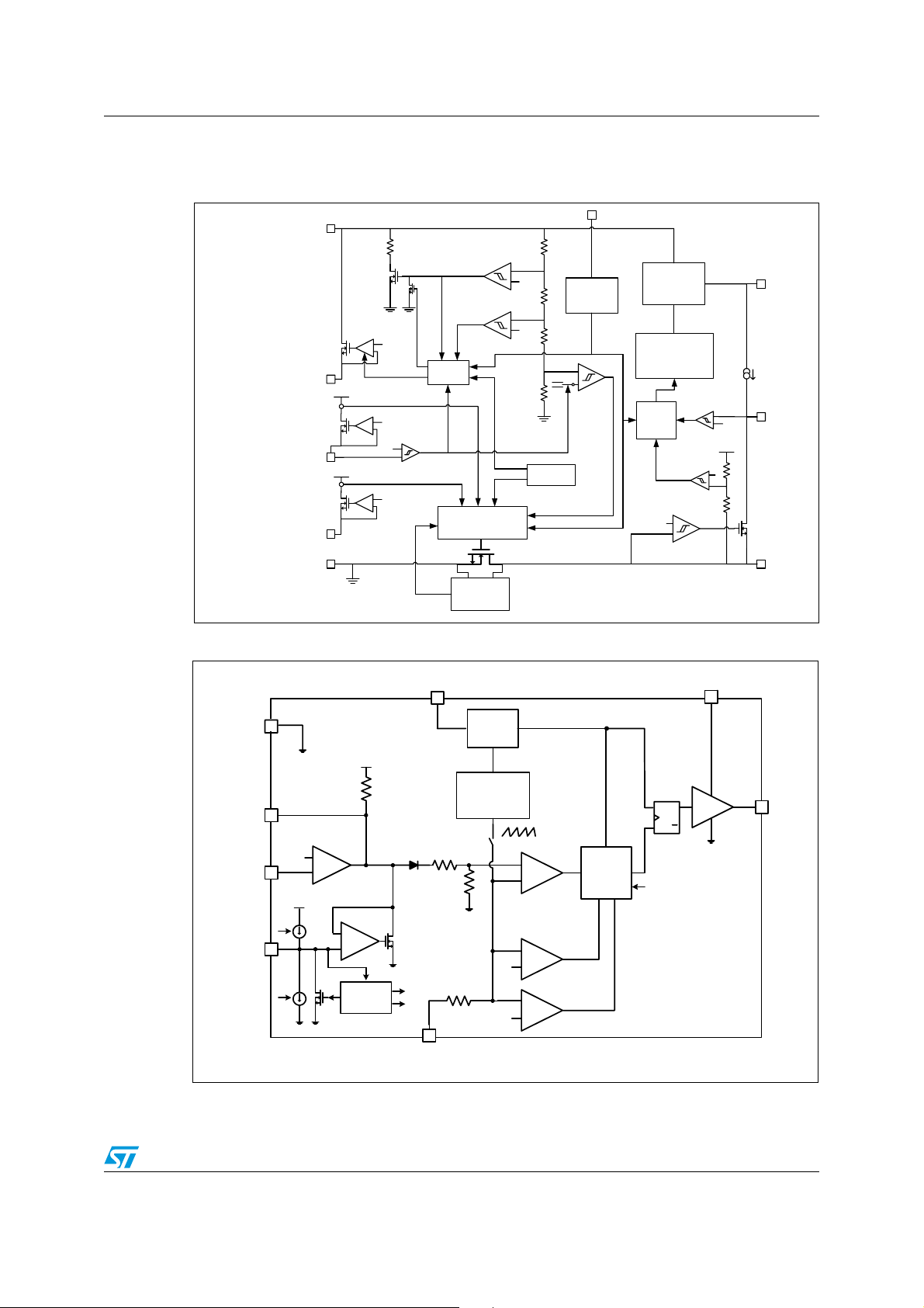
1.2 Block diagram
Figure 3. Block diagram of the PoE PD interface
Zener Ref
1.25V
1.4V
0.6V
Thermal
Protection
AUXII
AUX
Manager
threshold
-
+
UVLO
High Voltage
Startup
Regulator
DC/DC
controller
Power
Good Ctrl
Logic
1.5V
DC/DC
Enable
UVLO VCC
threshold
+
-
VCC
30uA
-
+
VCC
1.5V
+
-
nPGD
2V
VIN
RCLASS
AUXI_IRL
DCCL
3.3V
3.3V
24.5k
Detection
threshold
Classification
threshold
1.4V
+
-
EN
1.4V
+
-
1.4V
+
-
Interface
Manager
2V
+
-
Gate
Controller
-
+
-
+
VSS
Current and
Voltage
Sense
Figure 4. Block diagram of the current mode PWM controller
RT
AGND
COMP
FB
SS
10µA
10
charge
10
10µA
discharge
1.25V
A
A
3.3V
+
E/A
-
fast
discharge
+
-
LOGIC
3.3V
SS
2.5kOhm
discharge
charge
R
R
Oscillator
Slope
Compensation
0.5V
0.7V
+
PWM
-
+
OC1
-
+
OC2
-
45 A
45µA
PWM
logic
y Cycle by cycle over current
protection
y
80% duty cycle limit
(PM8800A)
y Leading Edge Blanking
Hiccup on OC2 or
y
persistent OC1
SET
S
Q
R
Q
CLR
DC/DC Enable
VCC
Driver
GND
GD
CS
5/35
Pins description and connection diagrams PM8800A
0
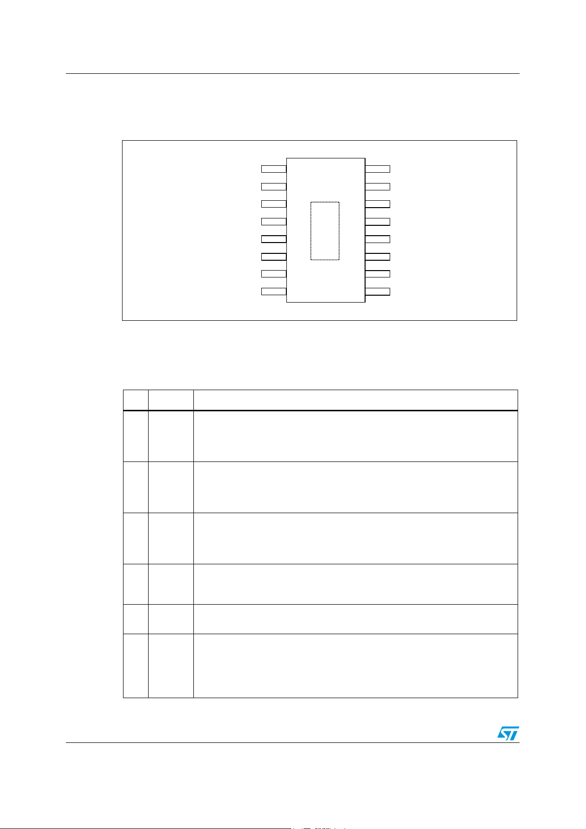
2 Pins description and connection diagrams
Figure 5. Pins connection (top view)
AUXII
RCLASS
AUXI_IRL
DCCL
2.1 Pin descriptions
Table 2. Pin description
Pin# Name Function
Oscillator timing resistor pin and synchronization input.
1RT
An external resistor connected from RT to AGND sets the oscillator frequency.
This pin will also accept narrow ac-coupled synchronization pulses from an
external clock.
RT
SS
VIN
VSS
16
15
14
4
13
11
1
HTSSOP-16
AGND
VFB
COMP
CS
nPGD
VCC
GD
9
GND
Soft-start input.
2SS
3AUXII
4VIN
5 RCLASS
6 AUXI_IRL
6/35
An external capacitor connected from SS and AGND and an internal
10 µA current source set the soft-start ramp rate. this pin is also used to set the
hiccup timer in case of overcurrent conditions. See Section 6 for detail.
Auxiliary source enable pin.
Use this pin to power up the DC/DC section only from the external source. The
auxiliary source can prevail over the PoE source depending on the value of the
resistor between this pin and the external source. See Section 7 for detail.
System high potential input.
The diode “OR” of PoE line and auxiliary sources connected to the PD, it is the
most positive input potential.
Classification resistor pin.
Connect a classification programming resistor between this pin and VSS.
In-rush current limit and auxiliary source enable pin.
Pulling up this pin to the auxiliary source will change the internal UVLO settings
and allow PD to be powered with voltage lower than nominal PoE voltages. In this
condition inrush current limit is set to default values. See Section 7 for details.
A resistance between this pin and VSS will set the level of inrush current limit.

PM8800A Pins description and connection diagrams
Table 2. Pin description (continued)
Pin# Name Function
DC current limit.
7DCCL
8 VSS System low potential input.
A resistor between DCCL and VSS will set the current limit for the interface
section of the PM8800A. It can be set to exceed the IEEE802.3af current limit.
Leave the pin open for standard IEEE 802.3af applications.
9GND
10 GD Output of the PWM controller. External power MOSFET gate driver output.
11 VCC
12
nPGD
13 CS
14 COMP
15 VFB
16 AGND
System return for the PWM converter.
It is the drain of the internal hot-swap power MOSFET.
Output of the internal high voltage regulator.
When the auxiliary transformer winding (if used) raises the voltage on this pin
above the regulation set point, the internal regulator will be switched off, reducing
the controller power dissipation.
Power good, active low signal.
A high to low transition indicates that the inrush current phase has been
completed, the internal hot swap MOSFET is fully closed and the SMPS portion of
the PM8800A is activated.
Current sense input.
Current sense input for current mode control and over-current protection. Current
limiting is obtained with a dedicated current sense comparator. If the CS pin
voltage exceeds 0.5 V the GD pin switches low for cycle-by-cycle current limiting.
Leading edge blanking is implemented to mask current spikes.
The output of the error amplifier and input of the Pulse Width Modulator.
COMP pull-up is provided by an internal 2.5 kΩ resistor which may be used to
bias an opto-coupler transistor.
Feedback signal.
Inverting input of the internal error amplifier. The non-inverting input is internally
connected to a 1.25 V reference.
If not used must be grounded to AGND.
Analog PWM supply return.
GND for sensitive analog circuitry including the SMPS current limit circuitry. Must
be connected to GND to improve noise immunity.
EP
Exposed pad.
Connect this to a board plane to improve heat dissipation; must be electrically
connected to VSS
7/35

Pins description and connection diagrams PM8800A
2.2 Thermal data
Table 3. Thermal data
Symbol Parameter Value Unit
R
thJA
T
MAX
T
STG
T
J
T
A
1. Package mounted on 4 layers 35 micron demoboard
Max thermal resistance junction to ambient
Maximum junction temperature 150 °C
Storage temperature range -40 to 150 °C
Junction temperature range -40 to 125 °C
Operative temperature range -40 to 85 °C
(1)
50 °C/W
8/35

PM8800A Electrical specifications
3 Electrical specifications
3.1 Absolute maximum ratings
Table 4. Absolute maximum ratings
Parameter Value Unit
VIN, GND to VSS -0.3 to 100 V
AUXI_IRL to VSS -0.3 to 100 V
DCCL, RCLASS to VSS -0.3 to 3.6 V
AUXII to AGND -0.3 to 100 V
COMP, SS to AGND -0.3 to 3.6 V
VFB, RT, CS to AGND -0.3 to 3.6 V
VCC, GD to AGND -0.3 to 15 V
nPGD to AGND -0.3 to 15 V
GND to AGND -0.3 to 0.3 V
Note: Absolute maximum ratings are limits beyond which damage to the device may occur.
9/35

Electrical specifications PM8800A
3.2 Electrical characteristic
Table 5. Electrical characteristics - interface section
(V
= 48 V, VCC = open, TA = 25 °C unless otherwise specified).
IN
Symbol Parameter Test conditions Min Typ Max Unit
Detection and classification
Signature enable VIN rising 1.5
Signature resistance 23.5
Signature disable
classification turn on
VIN rising 10.5
(1)
(1)
24.5 25.5
11.5 12.5
(1)
(1)
(1)
V
kΩ
V
Classification turn on
hysteresis
Classification turn-off V
RCLASS voltage during
classification
Supply current during
classification
Bias current
IIN V
supply current VIN = 48 V; VCC = 10 V 3 mA
IN
Under Voltage Lock-Out
V
UVLO_R
V
UVLO_F
UVLO release VIN rising 37 38.5 40
UVLO lock-out VIN falling 30
UVLO hysteresis 7.0 V
Hot swap MOSFET
R
DSON
MOSFET resistance 0.5 1
Default in-rush
current limit
Default in-rush
current limit
1.40 V
1.37
(1)
23 24.5
(1)
1.4 1.43
(1)
31.5 33.5 V
(1)
140 160
(1)
250 280
rising 21.5
IN
inside classification range 1.8 mA
V
IN
> 30 V 120
V
IN
15 V < V
< 30 V 220
IN
(1)
(1)
(1)
(1)
(1)
(1)
V
V
V
Ω
mA
mA
Default in-rush
current limit
Adjustable in-rush current
limit
1.5 V < V
R
AUXI_IRL
< 15 V 390
IN
= 82 kΩ 120
Default DC current limit 390
Adjustable DC
current limit precision
= From 15.4 kΩ to 82 kΩ -15
R
DCLL
10/35
(1)
(1)
(1)
(1)
440 490
140 160
440 490
-+15
(1)
(1)
(1)
(1)
mA
mA
mA
%

PM8800A Electrical specifications
Table 5. Electrical characteristics - interface section (continued)
(V
= 48 V, VCC = open, TA = 25 °C unless otherwise specified).
IN
Symbol Parameter Test conditions Min Typ Max Unit
Power good indication
Hot-swap VDS V
Hysteresis 1.45 V
Hot-swap VGS required
for power good
nPGD current source 25
nPGD
nPGD pull down
resistance
nPGD threshold nPGD rising 1.7
Auxiliary power
AUXI_IRL UVLO release VIN rising 15
AUX I
AUXI_IRL UVLO lock-out VIN falling 11.5
AUXI / IRL switch-over
threshold
falling 1.45
DS
(1)
1.60 1.75
Guaranteed by design 2 V
(1)
30 35 µA
nPGD low; I = -5 mA 0.5
V
AUXI_IRL
(1)
(1)
rising 2 V
22.3
16 17
(1)
12.5 13.5
(1)
(1)
(1)
(1)
(1)
V
V
V
V
V
AUX II
Bias voltage I
= 0 to -250 µA 0.85 1.1 1.4 V
AUXII
Lower threshold current 20 35 50 µA
Upper threshold current 80 100 120 µA
11/35

Electrical specifications PM8800A
Table 6. Electrical characteristics - SMPS section
(
V
= 48 V, VCC = open, TA = 25 °C unless otherwise specified).
IN
Symbol Parameter Test conditions Min Typ Max Unit
Oscillator
(1)
(1)
(1)
100 115
240 270
440 495
f
osc
Free running RT = open 85
= 88 kΩ 210
R
Frequency
programmability
T
= 33 kΩ 385
R
T
Ext. synch threshold 50 ns pulse 2.8 V
Error amplifier
V
EA
EA input voltage FB = COMP 1.21
(1)
1.25 1.29
GBW Gain bandwidth Guaranteed by design 10 MHz
G
COMP Sink current capability COMP to GND -8
DC gain Guaranteed by design 75 dB
0
(1)
-15 mA
Soft start
I
SS
Soft start current
Discharging -7
SS voltage After soft start 2.1
Charging 7
(1)
(1)
(1)
10 13
-10 -13
2.3 2.5
(1)
(1)
(1)
(1)
(1)
(1)
(1)
kHz
kHz
kHz
V
µA
µA
V
Current limit
Delay to output Guaranteed by design 20 ns
Cycle by cycle current
limit threshold voltage
Leading edge blanking
time
PWM comparator
Delay to output Guaranteed by design 25 ns
Minimum duty cycle 0
Maximum duty cycle 80 83
COMP to PWM gain Guaranteed by design 0.5
Output driver
Output high
Output low I
Fall time C
Rise time C
Peak source current
(1)
0.44
0.50 0.56
80 ns
(1)
(1)
= 100 mA;
I
GD
guaranteed by design
= -100 mA 0.25 0.5 V
GD
= 3.3 nF 35 ns
LOAD
= 3.3 nF 35 ns
LOAD
= 3.3 nF;
C
LOAD
guaranteed by design
Vcc-0.4 Vcc-0.7 V
800 mA
(1)
V
%
%
12/35

PM8800A Electrical specifications
Table 6. Electrical characteristics - SMPS section
(
V
= 48 V, VCC = open, TA = 25 °C unless otherwise specified).
IN
Symbol Parameter Test conditions Min Typ Max Unit
= 3.3 nF;
C
Peak sink current
Thermal shutdown
Shutdown temp.
LOAD
Guaranteed by design
st
level; Inrush phase only;
1
Guaranteed by design
1200 mA
130
2nd Level; guaranteed by design 160
°C
°C
Th. shutdown Hyst. 30
VCC regulation
Internal default VIN = 48 V; VCC = open 8
(1)
8.3 8.6
VCC
Current capability VIN = 48 V; GD = open 10
VCC
UVLO
Internal default
UVLO, release
Internal default;
UVLO, lock-out
rising; wrt VCC -400
V
CC
falling 6.4
V
CC
(1)
(1)
6.7 7.1
ICC VCC supply current VCC = 10 V 4 mA
regulator
V
CC
dropout
ICC = 5 mA; GD = open 2 V
Note: 1 These values applies over the full operating temperarure range.
2 Device thermal limitations could limit useful operating range.
3The V
additional external V
regulator is intended for internal use only as bias supply of PM8800A; any
CC
current has to be limited within the specified max current limit.
CC
°C
(1)
V
(1)
mA
-50 mV
(1)
V
13/35

Device description and operation PM8800A
4 Device description and operation
The PM8800A is a monolithic device embedding an IEEE 802.3af compliant PD interface
together with a current mode pulse width modulator to be used in all power over Ethernet
powered devices.
In addition to the standard.3af features, PM8800A anticipates some features of the forthcoming.3at standard, specifically targeting appliances or systems requiring higher power
with respect to the 12.95 W allowed by standard PSE.
The PD interface integrates the 24.5 kΩ signature resistor used in detection and disabled
during the rest of operating modes. Classification is done through an external resistor
detached when classification is over, in order to save power.
The PM8800A integrates standard compliant UVLO thresholds to determine normal operating mode (UVLO rising) or recognize disconnection (UVLO falling).
A graphical representation of the voltage thresholds and hysteresis during all the operating
phases is depicted in the following figure:
Figure 6. State diagram of the PM8800A interface depending on the input voltage
Powered
State of the PD
Classification
Detection
1.5V
11.5V10.1V 38.5V30.5V
Wait for turn-on
23V21V
31.5V
Input voltage
For input voltages in the range 1.5 to 11.5 V, PM8800A exposes a 24.5 kΩ resistance. After
detection is over, the internal resistor is disabled and the external classification resistor is
presented. When classification is over, the external resistor is disconnected and the
PM8800A wait for the input voltage to overpass the UVLO voltage.
The hot-swap MOSFET is specifically designed to have a low R
to contain the conduc-
DSon
tion losses and sustain up to 800 mA. A constant dissipated power method is used to limit
the current in the in-rush phase. The integrated in-rush current limit controls in a safe manner the current flowing through the MOSFET, shortening the duration of the hot-swap event
itself. Designers have the possibility to further limit the current in the in-rush by acting on the
proper programming resistor.
Designers have the possibility to set the limit of the current through the interface during normal operation. For non standard application, this limit exceeds the 350 mA foreseen by the
802.3af and can reach up to 800 mA.
14/35

PM8800A Device description and operation
PM8800A can work with power either from PoE networks or from auxiliary sources - like AC
adapters -. Alternative sources are present in PoE appliances where devices can work also
outside the context of the PoE networks or to ensure normal operation even if PoE becomes
unavailable. PM8800A limits the number of external components to handle the coexistence
of both PoE and auxiliary supplies.
External sources can be connected so to exploit the in-rush current limitation provided by
the MOSFET or enabling the PWM section, bypassing the interface section.
A state-of-the-art current mode pulse with modulator is embedded in the PM8800A to support low side single ended isolated and non isolated topologies. A high gain bandwidth product error amplifier is embedded for non isolated configuration.
PM8800A has a 80 % maximum duty cycle, featuring embedded slope compensation.
The PWM switching frequency of PM8800A is programmable with an appropriate resistor
and it is also capable of working with an external clock reference.
15/35

PD interface PM8800A
5 PD interface
5.1 Detection
In power over Ethernet systems, the PSE senses the connection to detect whether an IEEE
802.3af compatible device is plugged to the cable termination by applying a small voltage
(2.7 to 10 V) on the Ethernet cable and measuring in two successive steps the equivalent
resistance. During this phase, the Powered Device must present a resistance between
23.75 kΩ and 26.25 kΩ
PM8800A integrates a 24.5 kΩ signature resistor to simplify the design of PoE powered
Device appliances and to reduce the overall component count.
Signature resistor is in series to a pass transistor (see Figure 7) used to disconnect the
resistor itself upon completion of the detection phase.
The value of the integrated detection resistance has been selected taking into account also
the diode bridges typical voltage drop.
During detection, most of the circuits inside the PM8800A are disabled to minimize the
offset current.
Figure 7. PM8800A: reference schematic of the integrated 24.5 kΩ and resistor
disable logic
PM8800
A
VIN
VSS
11.5V
24.5k
+
-
16/35

PM8800A PD interface
5.2 Classification
Classification process in the IEEE 802.3af standard is optional for the powered device. This
feature allows PSE to plan and allocate the available power to the appliances connected to
the PoE network. IEEE 802.3af specification groups the need for power of the PD in 5
classes, one is reserved for future use. After successful detection, the PSE sets a constant
voltage between 15.5 V and 20.5 V for a maximum duration of 75 ms and senses the current
flowing through the cable to determine the PD's class.
The relevant thresholds in PM8800A are 11.5 V and 23 V, with a turn off hysteresis of 1.4 V.
To support the classification function, an equivalent programmable constant current
generator has been implemented. The following figure depicts a principle schematic of the
classification circuit. Just after the detection phase has been successfully completed, the
voltage of the RCLASS pin is set to the 1.4 V voltage reference and a pass transistor
connects the VIN pin to RCLASS pin.
Figure 8. PM8800A: reference schematic of the PoE classification logic
PM8800
VIN
RCLASS
A
Thermal_alarm
1.4V
+
EN
-
Class_enable
Aux_enabled
R
CLASS
VSS
Classification resistor can be detached by three main causes:
– An auxiliary power source (front or rear) has been connected (see Section 7),
– The device is in thermal protection
– The classification has been successfully completed.
Designers can set the current by changing the value of the external resistor according to the
following table.
17/35

PD interface PM8800A
Table 7. value of the external classification resistor for the different PD class of
power
IEEE 802.3af
CLASS PD power (W) R
0 0.44 - 12.95 Open 0 4
1 0.44 - 3.84 158 9 12
2 3.84 - 6.49 82.5 17 20
3 6.49 - 12.95 52.3 26 30
4 Reserved 36.5 36 44
CLASS
(Ω)
Classification current (mA)
min max
5.3 Under voltage lock-out
After the classification is completed, the PSE raises the voltage to provide the Power
Devices with the negotiated power. During the transition from low to operating voltage, the
internal UVLO is released and the hot-swap MOSFET is activated initiating the in-rush
sequence.
The IEEE 802.3af standard sets a maximum turn-on voltage (42 V) and the minimum turnoff voltage (30 V) for the PDs and indicates normal voltage drops across the Ethernet cable.
The PM8800A implements the UVLO mechanism by setting 2 internal thresholds on the
voltage across the VIN-VSS pins; one is to activate the hot-swap (V
is to switch off the hot-swap MOSFET upon detection of a supply voltage drop (V
from normal operating conditions.
No additional external components are required to comply with the IEEE 802.3af
requirements. Thermal protection alarm overrides the gate driving of the MOSFET
immediately switching off the MOSFET itself in case of device overheating. The hot-swap is
bypassed also in auxiliary source topology supplying directly the PWM and not requiring the
hot-swap to be active.
5.4 In rush current limit
Once the detection and classification phases have been successfully completed, the PSE
raises the voltage across the Ethernet cable. When the voltage difference between the VIN
and VSS is greater than the V
on and the DC-DC input capacitance is charged in a controlled way.
As depicted in the following figure, the current delivered by the hot-swap MOSFET during
inrush period is a function of the voltage drop between GND and VSS (hot-swap drain
source terminals). In more detail, the higher the voltage across the internal hot-swap, the
lower the current flowing trough it, so that the total dissipated power is almost constant
throughout the inrush phase, preventing the IC to reach the thermal protection limit.
UVLO_R
UVLO_R
), while the other
UVLO_F
)
threshold, the internal hot-swap MOSFET is switched
The lower current limitation is internally set at 140 mA and takes action when the voltage
GND-VSS is above 30 V. The second limit is set at 250 mA when GND-VSS voltage is
between 30 V and 15 V. When the voltage falls below 15 V, the limit switches to the higher
18/35

PM8800A PD interface
inrush current level, which is set by default at 440 mA. Connecting a resistor between VSS
and AUXI_IRL it's possible to adjust this limit to a lower value.
Figure 9. Relation between the hot-swap drain-source voltage and the default
Inrush current.
(mA)
Inrush Current
440
250
140
VIN-VSS
15V
30V
The maximum inrush current can be set by programming the value of the resistor on the
AUX_IRL pin. Depending on the chosen value there could be 3 steps (when the selected
max current is between 250 and 400 mA), 2 steps (when the selected max current is
between 140 and 250 mA) or a single step.
The formulae to select the desired inrush current is the following:
R
kΩ[]
IRL
11200
----------------------- -=
I
IRL
mA[]
The PM8800A useful programming range for the inrush current limitation is between
140 mA and 440 mA. Practical resistor value ranges between 25 kΩ and 82 kΩ.
Figure 10. Inrush current limit vs R
IRL
19/35

PD interface PM8800A
In the following picture a typical start sequence that can be observed in real circuits.
Figure 11. Typical start up sequence
Ch1 = 5 Vout, Ch2 = VSS - GND, Ch3 = Vcc, Ch4 = I input
Depending on the application, care must be put on the choice of the inrush current limit to
avoid that the voltage drop on the external Ethernet cable will cause UVLO conditions during
the charging phase of the bulk capacitor.
It is recommended to select this voltage drop (20 Ω max for 100 m of cable x I inrush) to be
lower than the UVLO hysteresis ( 7 V) in order to avoid hiccup turn on.
5.5 Continuos current limitation
PM8800A provide a default continuos current limitation of 440 mA. This is achieved by
leaving the pin DCCDL floating. A different DC current limit can be set by connecting a
resistor between DCCL and VSS whose value can be obtained by the following equation:
11200
RDCkΩ[]
-----------------------=
I
DC
mA[]
20/35

PM8800A PD interface
Figure 12. DC current vs R
DC
900
800
700
600
500
400
IDC [mA]
300
200
100
0
10 20 30 40 50 60 70 80
RDC [kohm]
This limitation is active after nPGD set and when the PD is supplied through the PoE or in
the Front connection (see Section 7)
The PM8800A useful programming range for the current limitation is between 150 mA and
800 mA. Practical resistor value ranges between 15 kΩ and 75 kΩ.
5.6 HV regulator startup
PM8800A embeds a high voltage start-up regulator to provide a controlled reference voltage
of 8.3 V to the Current mode PWM during its start-up phase.
The regulator output is connected to the VCC pin as well as to the DC DC section
In normal isolated topology, the VCC pin is diode connected to the auxiliary winding of the
transformer used for the flyback or forward configuration. When the voltage from the
transformer exceeds the regulated voltage, the high voltage regulator is shut off, reducing
the amount of power dissipated inside the PM8800A.
The external auxiliary voltage must higher then 8.3 V but must be also lower than 15 V
under all working conditions, to avoid the intervent of the internal protection clamp.
A VCC UVLO mechanism monitors the level of voltage on the VCC pin. When VCC voltage
exceeds the VCC
VCC voltage drops under its VCC
UVLO_R
the PWM controller is enabled and it remains enabled until the
UVLO_F
value.
21/35

PD interface PM8800A
5.7 Power good indication
The PM8800A embeds a power good circuit that is used to indicate that PWM input
capacitors are fully charged and that the switching regulator can start operation. The power
good circuit monitors the status of the internal hot-swap MOSFET and nPGD, an active low
signal is asserted when its V
good circuit includes hysteresis to allow the PM8800A to operate near the current limit point
without inadvertently disabling nPGD. The MOSFET voltage must increase to 3 V before
nPGD is disabled.
An internal comparator monitors the status of the nPGD pin and the PWM controller will be
running until the voltage at this pin goes above 2 V.
The power good indication is exposed at nPGD pin with a open drain, 45 Ω MOSFET so that
board designers can put a LED and a series current limiting resistor from the VCC pin to the
nPGD pin to indicate that the PD is powered from the PoE network.
Since the power good signal is internally used to activate the PWM controller, to avoid that
transients on the input voltage could produce intermittent operation of the PWM controller,
board designer can connect a capacitor C
mask the nPGD signal for a duration that can be estimate by the following equation:
voltage falls below 1.5 V and VGS rise above 2 V. The power
DS
between the nPGD pin and GND. This will
PGD
∆t µs()
2V C
----------------------------------------------------------=
0.03mA I
nF()⋅()
PGD
mA()+()
LED
where 30 µA is an internal current source that act as pull-up on the nPGD pin and I
current flowing through the external LED, if present.
LED
is the
22/35

PM8800A PWM section
6 PWM section
6.1 Error amplifier and loop compensation
The PM8800A addresses both isolated and non-isolated configuration by embedding a wide
band high gain error amplifier.
In non-isolated topology, the voltage to be regulated is connected to the FB pin - the
inverting input of the EA - through a resistor divider. The non inverting input of the EA is set
to a fixed reference value of 1.25 V. The output of the error amplifier is connected to the
COMP pin which is pulled up internally with a 2.5 kΩ resistor to a fixed reference of 3.3 V;
loop compensation can be done connecting an appropriate compensation network between
the FB pin and the COMP pin
Figure 13. Non-isolated feedback
A
PM8800
3.3V
2.5kOhm
E/A
COMP
VFB
-
+
1.25V
GND
AGND
ZCOMP
Vout
R
1
R
2
In typical isolated topology, the error amplifier is located outside the IC and the feedback
signal is taken on the collector of an opto coupler. The internal error amplifier is to be
bypassed connecting the FB pin to AGND. In order to minimize external components count
the opto coupler is directly connected to the COMP pin using the internal pull-up resistor as
bias for the opto coupler.
Figure 14. Isolated opto coupler feedback.
PM8800
A
3.3V
2.5k
E/A
COMP
VFB
-
+
1.25V
GND
AGND
R
Z
Vout
R
C
1
C
R
2
23/35

PWM section PM8800A
When a shunt regulator is used for output voltage regulation, the output voltage is set by the
ratio of resistors R1 and R2, see Figure 14 for details. The output voltage is given by the
following equation:
R
2
V
out
V
REF
⋅=
⎛⎞
1
------ -+
⎝⎠
R
1
where V
is the reference voltage of the shunt regulator chosen for the application.
REF
Loop compensation in typical isolated application is done by connecting an appropriate
compensation network around the external error amplifier.
A pull-up current source of few nA is internally connected to FB pin providing a safe switchoff of the DC DC converter in case of feedback disconnection.
6.2 Oscillator and sync capability
The internal oscillator frequency can be programmed by connecting an external resistor
between the RT and AGND pins. The relation between the oscillator frequency f
R
resistor is:
T
⎛⎞
kHz()100 1
f
osc
⋅=
⎝⎠
Figure 15. PWM frequency vs R
1000
900
800
700
600
[kHz]
500
OSC
F
400
300
200
100
125
--------------------------------------+
3kΩ R+
kΩ()
T
T
0
0 100 200 300 400
RT [kOhm ]
OSC
and the
The PWM switching frequency is equal to the programmed oscillator frequency.
24/35

PM8800A PWM section
The PM8800A can work also with a clock reference provided by an external source whose
frequency is higher than the one programmed by the R
resistor. The presence of the
T
external resistor is mandatory also when the reference is provided from outside the IC.
The external source must coupled to the RT with a 100 pF capacitor and have a minimum
peak amplitude of 2.8 V. Minimum pulse width of 50 ns has to be assured for proper
operation.
When synchronized the PWM frequency is equal to the external clock reference.
6.3 Soft start
The soft-start feature of the PM8800A allows the load voltage to ramp-up in a safe and
controlled manner. This is achieved by a 10 µA internal current source charging an external
C
capacitor connected to the SS pin, which progressively increases the duty cycle of the
ss
PWM pulse, since the reference of the error amplifier is clamped with this value. Duration of
the start-up time and external capacitor are linked by the following relation:
tssms()0.23 CSSnF()⋅=
SS voltage is actively kept at 2.3 V by the internal control circuitry, which manages also
over-current and fault conditions.
Figure 16. Typical soft start waveform
Ch1 = 5Vout, Ch2 = soft start, Ch4 = I input
25/35

PWM section PM8800A
6.4 PWM comparator / slope compensation
In typical isolated operation, current is sensed on a sense resistor Rs put between the
source of the primary side MOSFET and GND pin, while for non-isolated topology it is often
sensed on a proper resistor put on the source of a low-side MOSFET.
The PWM comparator produces the PWM duty cycle by comparing the Rs ramp signal on
CS with an error voltage derived from the error amplifier output.
The error amplifier output voltage at the COMP pin is offset by 0.7 V and then further
attenuated by a 2:1 resistor divider before it is presented to the PWM comparator input.
The PWM duty cycle increases with the voltage at the COMP pin. The controller output duty
cycle reduces to zero when the COMP pin voltage drops below approximately 0.7 V.
For duty cycles greater than 50 %, current mode control loops are subject to sub-harmonic
oscillation. The PM8800A fixes the maximum duty dycle at 80 % and implements a slope
compensation technique consisting on adding an additional fixed slope voltage ramp to the
signal at the CS pin. This is achieved by injecting a 45 µA sawtooth current into the current
sense signal path on an integrated 2 kΩ resistor.
Additional slope compensation may be added by increasing the source impedance of the
current sense signal with an external resistor between the CS pin and the source of the
current sense signal. The net effect in this case is to increase the slope of the voltage ramp
at the PWM comparator terminals.
6.5 Current limiting
The current sensed through the CS pin is compared to two fixed levels of 0.5 V and 0.7 V.
The lower level is used to perform a cycle-by-cycle current limit, terminating the PWM pulse.
In case of recurring overload a timing structure is activated through SS pin, sourcing a small
current of about 1 µA on SS capacitor. The voltage on SS rises whenever during a PWM
cycle an over current event occurs, while decreases to the default voltage (2.3 V) if it does
not.
If SS voltage reaches 2.8 V, a slow hiccup is performed sinking 1 µA from SS, and shutting
down the gate driver until the SS capacitor is fully discharged.
Then a new soft-start procedure is performed.
26/35

PM8800A PWM section
Figure 17. Short circuit on the output
Ch1 = 5Vout, Ch2 = SoftStart, Ch3 = VSS - GND, Ch4 = I input
When a severe over current occurs, like a short circuit of an internal power component, and
0.7 V level is reached on CS, the gate driver is instantaneously shut down and a fast hiccup
cycle is performed. When the 10 µA sink current fully discharges the SS capacitor, a new
soft-start procedure is performed.
In case of persistent severe over current, the control logic tries 4 cycles of fast hiccup before
shutting down the PWM controller at all.
To restart the device, after removing the cause of over current, VIN must be lowered under
UVLO level.
27/35

PWM section PM8800A
Figure 18. Internal short circuit
1
Ch1 = 5 Vout, Ch2 = SoftStart, Ch4= I input
2
6.6 Leading edge blanking
The sense current waveform often observes large spikes on the leading edge. This is due to
rectifier recovery and/or interwinding capacitance in the power transformer. If not
attenuated, this transient can prematurely terminate the output pulse. A simple RC filter whose time constant is approximately equal to the spike duration - is usually adequate to
suppress this spike.
An internal blanking time has been anyway integrated in order to prevent false overcurrent
detection to terminate the PWM waveform. This is done by a masking logic, active for
duration of 70 ns after the turn-on time of the primary side MOSFET.
3
4
6.7 Thermal protection
PM8800A has a two level thermal protection referred to the internal junction temperature.
First limit is set to 130 °C and limits the current into the hot-swap MOSFET to 140 mA every
time the voltage difference between VSS and GND is higher than 3 V.
The second limit is set to 160 °C and is always active. When this threshold is overtaken, the
hot-swap is opened and the PWM controller is switched-off.
28/35

PM8800A Auxiliary sources
7 Auxiliary sources
The majority of powered devices is designed to work with power from either PoE network or
auxiliary sources. Even though having both sources simultaneously connected is not the
normal operating case, the presence of an auxiliary supply allows PDs to be used also when
the PoE is not available or not sufficient. This is particularly true for appliances requiring
more than 12.95 W connected to 802.3af compliant PSE.
High degree of flexibility is granted by the PM8800A for designs based on external sources.
As depicted in the following figure there are two available options for connecting auxiliary
sources to the PM8800A. One possibility consists in diode O-ring the auxiliary source into
the PM8800A PoE pins (VIN and VSS) referred to "Option I ". In the second alternative,
referred to "Option II" the external supply voltage is diode ORed into the PWM section of the
device.
Figure 19. Alternatives for auxiliary source connection
Option I
VIN
AUXI_IRL
DCCL
RCLASS
VSS
PM8800
AUXII
COMP
nPGD
A
GND
AGND
VCC
GD
CS
VFB
SS
RT
Option II
The two options differ for the in-rush and DC current protection, for the allowed auxiliary
source voltage range, power sequence and prevalence of the external source with respect
to the PoE one.
Option I configuration has been designed to take advantage of the inherent in-rush and DC
current protection also when working with voltages from external power supplies.
When the auxiliary source is connected prior to PD detection by the PSE and has a voltage
above the V
UVLO_R
(38-57 V), the internal UVLO is released and the MOSFET is switched
on, starting the inrush phase. Inrush and DC current limit can be programmed by respective
external resistors see Section 5.4 and Section 5.5.
Internal under voltage lock out threshold can be lowered by connecting the auxiliary source
to the AUXI_IRL pin. Wall adapter with supply voltage lower than 38 V can be used, still
profiting from the inrush and DC current limit provided by the hot-swap MOSFET.
29/35

Auxiliary sources PM8800A
The minimum external voltage to be used in this configuration is about 16 V.
Option I connection is activated when the voltage at the relevant pin is higher than 2 V and a
current I
I
AUXI
higher than 70 µA is forced into the pin.
AUXI
V
– 2–
AUXIVD
-------------------------------------- -
R
AUXI
70µA≥=
The AUXI_IRL pin can be connected to the auxiliary source through a diode being the
current internally limited to about 300 µA.
It is important to highlight that UVLO override and inrush current limit are mutually exclusive,
and when UVLO is overridden, default inrush current limit is provided. The PSE will not
detect the presence of a valid PD, since the PoE diode bridges are reversed biased.
When the auxiliary source is connected after the inrush phase, two possibilities arise
depending on the voltage of the external power supply. If the voltage is lower than the one
from PoE, the diode is reverse biased and PSE will keep on supplying the PD. If the auxiliary
source has a voltage greater than the PoE, the PoE diode bridge will be reverse biased and
auxiliary source will supply the PD. In case the voltages are comparable, current sharing
occurs between the sources according to their respective source resistance.
The Option II configuration bypasses the PD interface and connects directly the external
source to the PWM section. This type of connection is not limited by the internal current limit
circuits and therefore is more suitable for lower auxiliary voltages.
Internal under voltage lock out threshold will be lowered by connecting the auxiliary source
to the AUXII pin. The minimum external voltage to be used in this configuration is about
12 V.
Note that inrush current in this case is not limited and an external solution must be found:
the simplest solution is to put a low value resistor in series, but this lower the converter
efficiency. More efficient solution is the use of a MOSFET as power switch, able to limit the
current during the charging phase, and to add only few milliohm in series during normal
operation.
Main advantage of this connection is the "prevalence" over PoE voltage, that can be
obtained pulling up AUXII pin with a R
resistor and forcing a current into the pin greater
AUXII
than 100 µA (see following equation). In this case the PD interface is switched off regardless
the presence of PoE voltage.
I
AUXII
------------------------------------------ -
R
AUXII
100µA≥=
V
– 1.1·–
AUXIIVD
AUXII can be connected directly to the auxiliary voltage through a diode. The current in this
case is internally limited to about 250 µA.
If a prevalent AUXII is detected the PD interface is switched off, the hot swap MOSFET is
opened regardless the PoE voltage level.
30/35

PM8800A Auxiliary sources
If the current forced into AUXII pin is lower than 60 µA, the internal under voltage lock out
threshold will be lowered but AUXII connection will be not prevalent to the PoE; in this case
power to the DC/DC converter will be drawn from the source that has been applied first.
In case of very low auxiliary voltage (i.e. lower than 15 V) is recommended to supply VCC
directly with the auxiliary voltage through a bypass diode, in order to assure a proper
operation of the pwm section of PM8800A.
Figure 20. Switch over between 48 V PoE and 12 V AUXII auxiliary adapter
Ch2
Ch3
Ch1 = 5 Vout, Ch2 = Aux voltage, Ch3 = internal primary voltage, Ch4 = Aux input current
31/35

Package mechanical data PM8800A
8 Package mechanical data
In order to meet environmental requirements, ST offers these devices in ECOPACK®
packages. These packages have a lead-free second level interconnect. The category of
second Level Interconnect is marked on the package and on the inner box label, in
compliance with JEDEC Standard JESD97. The maximum ratings related to soldering
conditions are also marked on the inner box label. ECOPACK is an ST trademark.
ECOPACK specifications are available at: www.st.com.
32/35

PM8800A Package mechanical data
8.1 HTSSOP16 mechanical data
Figure 21. HTSSOP16 mechanical data and package dimensions
DIM.
A 1.20 0.047
A1 0.15 0.006
A2 0.80 1.0 1.05 0.032 0.039 0.041
b 0.19 0.30 0.007 0.012
c 0.09 0.20 0.004 0.008
D 4.90 5.00 5.10 0.193 0.197 0.201
D1 3.00 0.118
E 6.20 6.40 6.60 0.244 0.252 0.260
E1 4.30 4.40 4.50 0.169 0.173 0.177
E2 3.00 0.118
e 0.65 0.026
L 0.45 0.60 0.75 0.018 0.024 0.030
L1 1.00 0.039
k 0 8 0.315
aaa 0.10 0.004
mm inch
min typ max min typ max
OUTLINE AND
MECHANICAL DATA
(Exposed Pad)
HTSSOP16
33/35

Revision history PM8800A
9 Revision history
Table 8. Document revision history
Date Revision Changes
17-Sep-2007 1 Initial release
20-Feb-2008 2 Content reworked in order to improve readability
34/35

PM8800A
Please Read Carefully:
Information in this document is provided solely in connection with ST products. STMicroelectronics NV and its subsidiaries (“ST”) reserve the
right to make changes, corrections, modifications or improvements, to this document, and the products and services described herein at any
time, without notice.
All ST products are sold pursuant to ST’s terms and conditions of sale.
Purchasers are solely responsible for the choice, selection and use of the ST products and services described herein, and ST assumes no
liability whatsoever relating to the choice, selection or use of the ST products and services described herein.
No license, express or implied, by estoppel or otherwise, to any intellectual property rights is granted under this document. If any part of this
document refers to any third party products or services it shall not be deemed a license grant by ST for the use of such third party products
or services, or any intellectual property contained therein or considered as a warranty covering the use in any manner whatsoever of such
third party products or services or any intellectual property contained therein.
UNLESS OTHERWISE SET FORTH IN ST’S TERMS AND CONDITIONS OF SALE ST DISCLAIMS ANY EXPRESS OR IMPLIED
WARRANTY WITH RESPECT TO THE USE AND/OR SALE OF ST PRODUCTS INCLUDING WITHOUT LIMITATION IMPLIED
WARRANTIES OF MERCHANTABILITY, FITNESS FOR A PARTICULAR PURPOSE (AND THEIR EQUIVALENTS UNDER THE LAWS
OF ANY JURISDICTION), OR INFRINGEMENT OF ANY PATENT, COPYRIGHT OR OTHER INTELLECTUAL PROPERTY RIGHT.
UNLESS EXPRESSLY APPROVED IN WRITING BY AN AUTHORIZED ST REPRESENTATIVE, ST PRODUCTS ARE NOT
RECOMMENDED, AUTHORIZED OR WARRANTED FOR USE IN MILITARY, AIR CRAFT, SPACE, LIFE SAVING, OR LIFE SUSTAINING
APPLICATIONS, NOR IN PRODUCTS OR SYSTEMS WHERE FAILURE OR MALFUNCTION MAY RESULT IN PERSONAL INJURY,
DEATH, OR SEVERE PROPERTY OR ENVIRONMENTAL DAMAGE. ST PRODUCTS WHICH ARE NOT SPECIFIED AS "AUTOMOTIVE
GRADE" MAY ONLY BE USED IN AUTOMOTIVE APPLICATIONS AT USER’S OWN RISK.
Resale of ST products with provisions different from the statements and/or technical features set forth in this document shall immediately void
any warranty granted by ST for the ST product or service described herein and shall not create or extend in any manner whatsoever, any
liability of ST.
ST and the ST logo are trademarks or registered trademarks of ST in various countries.
Information in this document supersedes and replaces all information previously supplied.
The ST logo is a registered trademark of STMicroelectronics. All other names are the property of their respective owners.
© 2008 STMicroelectronics - All rights reserved
STMicroelectronics group of companies
Australia - Belgium - Brazil - Canada - China - Czech Republic - Finland - France - Germany - Hong Kong - India - Israel - Italy - Japan -
Malaysia - Malta - Morocco - Singapore - Spain - Sweden - Switzerland - United Kingdom - United States of America
www.st.com
35/35
 Loading...