

Page 1
Dual synchronous step-down controller
with adjustable output voltages plus LDO
Features
■ 6 V to 36 V input voltage range
■ Adjustable output voltages
■ 5V LDO delivers 100 mA peak current
■ 1.237 V ± 1 % reference voltage available
externally
■ Current sensing using low side MOSFETs
R
■ Valley current sensing
■ Soft-start internally fixed at 2ms
■ Soft output discharge
■ Latched OVP and UVP
■ Selectable pulse skipping at light loads
■ Selectable minimum frequency (33 kHz) in
pulse skip mode
■ 5mW maximum quiescent power
■ Independent power good signals
■ Output voltage ripple compensation
■ Thermal shutdown
Applications
■ Embedded computer system
■ FPGA system power
■ Industrial applications on 24 V
■ High performance and high density DC/DC
modules
DS(on)
PM6680A
VFQFPN-32 5X5
Description
PM6680A is a dual step-down controller
specifically designed to provide extremely high
efficiency conversion, with loss less current
sensing technique. The constant on-time
architecture assures fast load transient response
and the embedded voltage feed-forward provides
nearly constant switching frequency operation. An
embedded integrator control loop compensates
the DC voltage error due to the output ripple.
Pulse skipping technique increases efficiency at
very light load. Moreover a minimum switching
frequency of 33 kHz is selectable to avoid audio
noise issues. The PM6680A provides a selectable
switching frequency, allowing three different
values of switching frequencies for the two
switching sections. The output voltages OUT1
and OUT2 can be adjusted from 0.9 V to 5 V and
from 0.9 V to 3.3 V respectively.
Table 1. Device summary
Order codes Package Packaging
PM6680A
VFQFPN-32 5X5 (exposed pad)
PM6680ATR Tape and reel
December 2007 Rev 2 1/48
Tu b e
www.st.com
48
Page 2

Contents PM6680A
Contents
1 Block diagram . . . . . . . . . . . . . . . . . . . . . . . . . . . . . . . . . . . . . . . . . . . . . . 3
2 Pin settings . . . . . . . . . . . . . . . . . . . . . . . . . . . . . . . . . . . . . . . . . . . . . . . . 4
2.1 Connections . . . . . . . . . . . . . . . . . . . . . . . . . . . . . . . . . . . . . . . . . . . . . . . . 4
2.2 Functions . . . . . . . . . . . . . . . . . . . . . . . . . . . . . . . . . . . . . . . . . . . . . . . . . . 5
3 Electrical data . . . . . . . . . . . . . . . . . . . . . . . . . . . . . . . . . . . . . . . . . . . . . . 8
3.1 Maximum rating . . . . . . . . . . . . . . . . . . . . . . . . . . . . . . . . . . . . . . . . . . . . . 8
3.2 Thermal data . . . . . . . . . . . . . . . . . . . . . . . . . . . . . . . . . . . . . . . . . . . . . . . 8
4 Electrical characteristics . . . . . . . . . . . . . . . . . . . . . . . . . . . . . . . . . . . . . 9
5 Typical operating characteristics . . . . . . . . . . . . . . . . . . . . . . . . . . . . . 12
6 Application schematic . . . . . . . . . . . . . . . . . . . . . . . . . . . . . . . . . . . . . . 17
7 Device description . . . . . . . . . . . . . . . . . . . . . . . . . . . . . . . . . . . . . . . . . 18
7.1 Constant On time PWM control . . . . . . . . . . . . . . . . . . . . . . . . . . . . . . . . 18
7.2 Constant On time architecture . . . . . . . . . . . . . . . . . . . . . . . . . . . . . . . . . 20
7.3 Output ripple compensation and loop stability . . . . . . . . . . . . . . . . . . . . . 21
7.4 Pulse skip mode . . . . . . . . . . . . . . . . . . . . . . . . . . . . . . . . . . . . . . . . . . . . 22
7.5 No-audible skip mode . . . . . . . . . . . . . . . . . . . . . . . . . . . . . . . . . . . . . . . . 23
7.6 Current limit . . . . . . . . . . . . . . . . . . . . . . . . . . . . . . . . . . . . . . . . . . . . . . . 24
7.7 Soft start and soft end . . . . . . . . . . . . . . . . . . . . . . . . . . . . . . . . . . . . . . . 25
7.8 Gate drivers . . . . . . . . . . . . . . . . . . . . . . . . . . . . . . . . . . . . . . . . . . . . . . . 26
7.9 Reference voltage and bandgap . . . . . . . . . . . . . . . . . . . . . . . . . . . . . . . 27
7.10 Internal linear regulator . . . . . . . . . . . . . . . . . . . . . . . . . . . . . . . . . . . . . . 27
7.11 Power up sequencing and operative modes . . . . . . . . . . . . . . . . . . . . . . . 28
8 Monitoring and protections . . . . . . . . . . . . . . . . . . . . . . . . . . . . . . . . . . 29
2/48
Page 3

PM6680A Contents
9 Design guidelines . . . . . . . . . . . . . . . . . . . . . . . . . . . . . . . . . . . . . . . . . . 30
9.1 Switching frequency . . . . . . . . . . . . . . . . . . . . . . . . . . . . . . . . . . . . . . . . . 30
9.2 Inductor selection . . . . . . . . . . . . . . . . . . . . . . . . . . . . . . . . . . . . . . . . . . . 30
9.3 Output capacitor . . . . . . . . . . . . . . . . . . . . . . . . . . . . . . . . . . . . . . . . . . . . 31
9.4 Input capacitors selection . . . . . . . . . . . . . . . . . . . . . . . . . . . . . . . . . . . . . 32
9.5 Power MOSFETS . . . . . . . . . . . . . . . . . . . . . . . . . . . . . . . . . . . . . . . . . . . 33
9.6 Closing the integrator loop . . . . . . . . . . . . . . . . . . . . . . . . . . . . . . . . . . . . 35
9.7 Other parts design . . . . . . . . . . . . . . . . . . . . . . . . . . . . . . . . . . . . . . . . . . 39
9.8 Design example . . . . . . . . . . . . . . . . . . . . . . . . . . . . . . . . . . . . . . . . . . . . 40
10 Package mechanical data . . . . . . . . . . . . . . . . . . . . . . . . . . . . . . . . . . . . 45
11 Revision history . . . . . . . . . . . . . . . . . . . . . . . . . . . . . . . . . . . . . . . . . . . 47
3/48
Page 4
Block diagram PM6680A
V
V
N
V
V
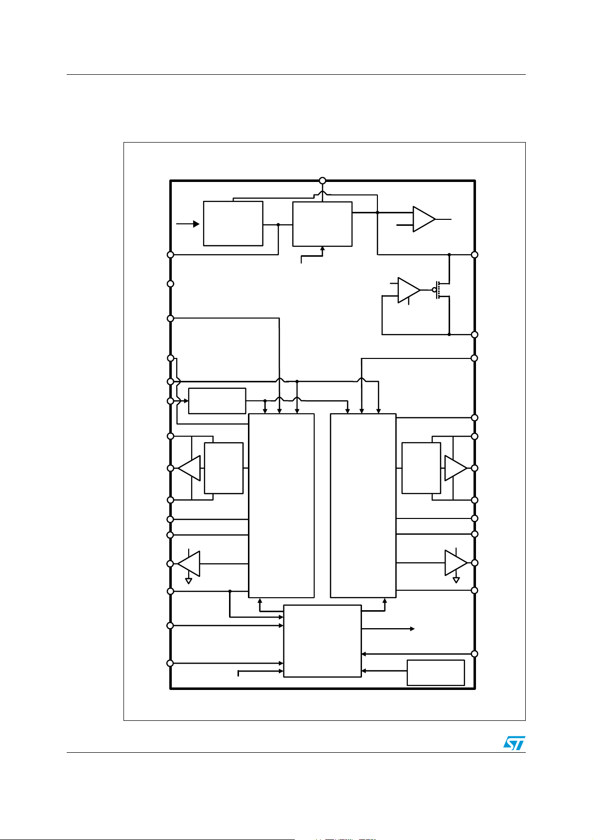
1 Block diagram
Figure 1. Functional block diagram
IN
REF
C
FB2
OUT2
SKIP
FSEL
BOOT2
HGATE2
PHASE2
COMP2
V
CC
FREQUENCY
SELECTOR
LDO5
REFERENCE
GENERATOR
LEVEL
SHIFTER
REF
LDO5 ENABLE
OUT2
SMPS
CONTROLLER
5V
LINEAR
REGULATOR
CONTROLLER
4.8V
OUT1
SMPS
4V
+
-
UVLO
SHIFTER
+
-
LEVEL
UVLO
LDO5
5SW
FB1
OUT1
BOOT1
HGATE1
PHASE1
CSENSE1
COMP1
LDO5
LGATE2
SHDN
EN2
UVLO
STARTUP
CONTROLLER
TERMIC
FAULT
LDO5 ENABLE
TERMIC
CONTROLLER
LGATE1
PGOOD1
EN1
4/48
Page 5
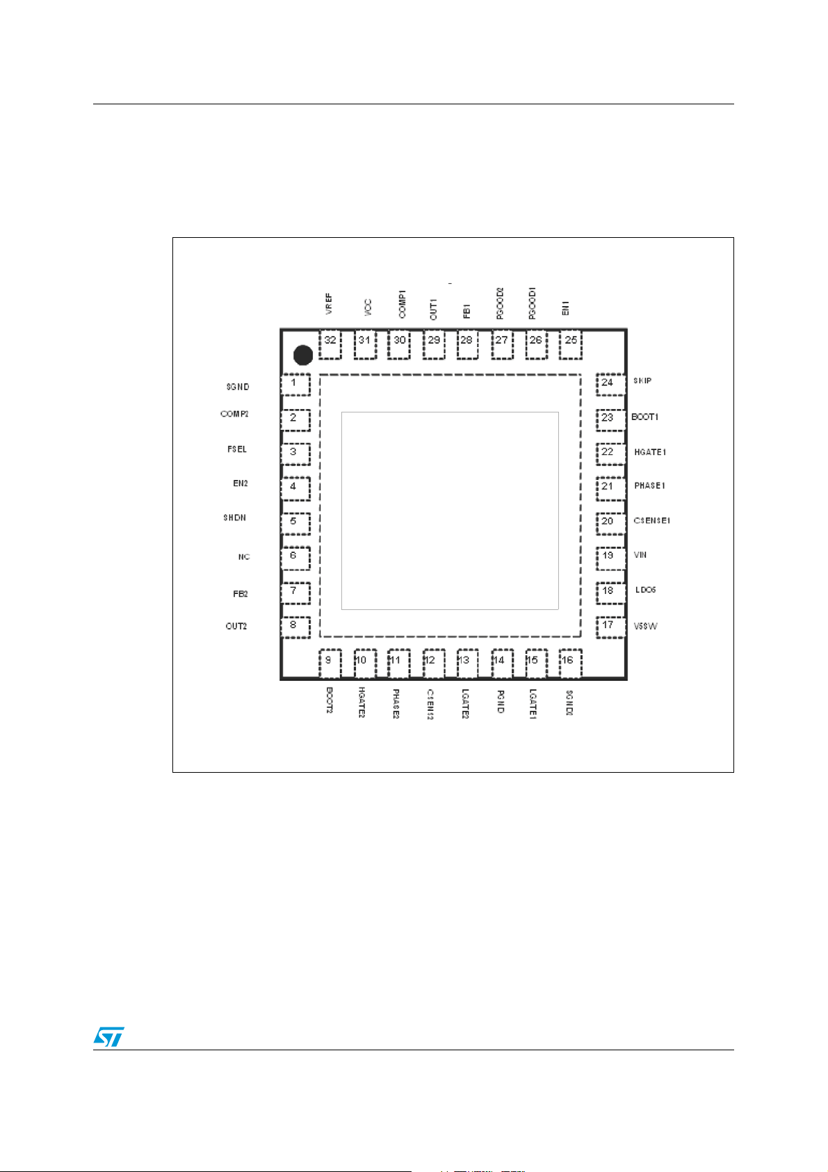
PM6680A Pin settings
2 Pin settings
2.1 Connections
Figure 2. Pin connection (through top view)
1
PM6680A
5/48
Page 6
Pin settings PM6680A
2.2 Functions
Table 2. Pin functions
N° Pin Function
Signal ground. Reference for internal logic circuitry. It must be connected to the
1 SGND1
2 COMP2 DC voltage error compensation pin for the switching section 2
3 FSEL
4EN2
5 SHDN
signal ground plan of the power supply. The signal ground plan and the power
ground plan must be connected together in one point near the PGND pin.
Frequency selection pin. It provides a selectable switching frequency, allowing three
different values of switching frequencies for the switching sections.
Enable input for the switching section 2.
• The section 2 is enabled applying a voltage greater than 2.4 V to this pin.
• The section 2 is disabled applying a voltage lower than 0.8 V.
When the section is disabled the High Side gate driver goes low and Low Side gate
driver goes high. If both EN1 and EN2 pins are low and SHDN pin is high the device
enters in standby mode.
Shutdown control input.
• The device switch off if the SHDN voltage is lower than the device off thershold
(Shutdown mode)
• The device switch on if the SHDN voltage is greater than the device on threshold.
The SHDN pin can be connected to the battery through a voltage divider to program
an undervoltage lockout. In shutdown mode, the gate drivers of the two switching
sections are in high impedance (high-Z).
6 NC Not connected.
7FB2
8OUT2
9BOOT2
Feedback input for the switching section 2 This pin is connected to a resistive
voltage-divider from OUT2 to PGND to adjust the output voltage from 0.9 V to 3.3 V.
Output voltage sense for the switching section 2.This pin must be directly connected
to the output votage of the switching section.
Bootstrap capacitor connection for the switching section 2. It supplies the high-side
gate driver.
10 HGATE2 High-side gate driver ouput for section 2. This is the floating gate driver output.
11 PHASE2
Switch node connection and return path for the high side driver for the section 2.It is
also used as negative current sense input.
Positive current sense input for the switching section 2. This pin must be connected
12 CSENSE2
through a resistor to the drain of the synchronous rectifier (R
sensing) to obtain
DSON
a positive current limit threshold for the power supply controller.
13 LGATE2 Low-side gate driver output for the section 2.
14 PGND
Power ground. This pin must be connected to the power ground plan of the power
supply.
15 LGATE1 Low-side gate driver output for the section 1.
16 SGND2
Signal ground for analog circuitry. It must be connected to the signal ground plan of
the power supply.
6/48
Page 7

PM6680A Pin settings
Table 2. Pin functions (continued)
N° Pin Function
Internal 5 V regulator bypass connection.
• If V5SW is connected to OUT5 (or to an external 5 V supply) and V5SW is greater
17 V5SW
than 4.9 V, the LDO5 regulator shuts down and the LDO5 pin is directly connected to
OUT5 through a 3 Ω (max) switch.
If V5SW is connected to GND, the LDO5 linear regulator is always on.
18 LDO5
19 VIN
20 CSENSE1
21 PHASE1
22 HGATE1 High-side gate driver ouput for section 1. This is the floating gate driver output.
23 BOOT1
24 SKIP
25 EN1
26 PGOOD1
27 PGOOD2
28 FB1
29 OUT1
5V internal regulator output. It can provide up to 100 mA peak current. LDO5 pin
supplies embedded low side gate drivers and an external load.
Device supply voltage input and battery voltage sense. A bypass filter
(4 Ω and 4.7 µF) between the battery and this pin is recommended.
Positive current sense input for the switching section 1. This pin must be connected
through a resistor to the drain of the synchronous rectifier (R
a positive current limit threshold for the power supply controller.
Switch node connection and return path for the high side driver for the section 1.It is
also used as negative current sense input.
Bootstrap capacitor connection for the switching section 1. It supplies the high-side
gate driver.
Pulse skipping mode control input.
• If the pin is connected to LDO5 the PWM mode is enabled.
• If the pin is connected to GND, the pulse skip mode is enabled.
• If the pin is connected to VREF the pulse skip mode is enabled but the switching
frequency is kept higher than 33 kHz (No-audible puse skip mode).
Enable input for the switching section 1.
• The section 1 is enabled applying a voltage greater than 2.4 V to this pin.
• The section 1 is disabled applying a voltage lower than 0.8 V.
When the section is disabled the High Side gate driver goes low and Low Side gate
driver goes high.
Power Good ouput signal for the section 1. This pin is an open drain ouput and when
the ouput of the switching section 1 is out of +/- 10 % of its nominal value.It is pulled
down.
Power Good ouput signal for the section 2. This pin is an open drain ouput and when
the ouput of the switching section 2 is out of +/- 10 % of its nominal value.It is pulled
down.
Feedback input for the switching section 1. This pin is connected to a resistive
voltage-divider from OUT1 to PGND to adjust the output voltage from 0.9 V to 5.5 V.
Output voltage sense for the switching section 1.This pin must be directly connected
to the output votage of the switching section.
sensing) to obtain
DSON
30 COMP1 DC voltage error compensation pin for the switching section 1.
31 VCC
32 VREF
Device supply voltage pin. It supplies all the internal analog circuitry except the gate
drivers (see LDO5). Connect this pin to LDO5.
Internal 1.237 V high accuracy voltage reference. It can deliver 50 µA. Bypass to
SGND with a 100 nF capacitor to reduce noise.
7/48
Page 8

Electrical data PM6680A
3 Electrical data
3.1 Maximum rating
Table 3. Absolute maximum ratings
Parameter Value Unit
V5SW, LDO5 to PGND -0.3 to 6 V
VIN to PGND -0.3 to 36 V
HGATEx and BOOTx, to PHASEx -0.3 to 6 V
(1)
PHASEx to PGND -0.6
CSENSEx , to PGND -0.6 to 42 V
CSENSEx to BOOTx -6 to 0.3 V
LGATEx to PGND -0.3
FBx, COMPx, SKIP, , FSEL,,VREF to SGND1,SGND2 -0.3 to Vcc+0.3 V
PGND to SGND1,SGND2 -0.3 to 0.3 V
to36
(2)
to LDO5 +0.3
V
V
SHDN,PGOODx, OUTx, VCC, ENx to SGND1,SGND2 -0.3 to 6 V
Power Dissipation at T
Maximum withstanding Voltage range test condition:
CDF-AEC-Q100-002- “Human Body Model” acceptance
criteria: “Normal Performance”
1. PHASE to PGND up to -2.5 V for t < 10 ns
2. LGATEx to PGND up to -1 V for t < 40 ns
3.2 Thermal data
Table 4. Thermal data
Symbol Parameter Value Unit
R
T
thJA
STG
T
J
Thermal resistance junction to ambient 35 °C/W
Storage temperature range -40 to 150 °C
Junction operating temperature range -40 to 125 °C
= 25ºC 2.8 W
A
VIN ±1000
Other pins ±2000
V
8/48
Page 9
PM6680A Electrical characteristics
4 Electrical characteristics
Table 5. Electrical characteristics
T
= -40 °C to 125 °C, unless otherwise specified. All parameters at operating temperature
A
extremes are guaranteed by design and statistical analysis (not production tested).
Symbol Parameter Test condition Min Typ Max Unit
Supply section
VIN Input voltage range Vout = Vref, LDO5 in regulation 5.5 36 V
V
CC
V
V5SW
V
V5SW
R
DS(on)
Pin
Ish
Isb
Shutdown section
IC supply voltage 4.5 5.5 V
Turn-ON voltage threshold 4.8 4.9 V
Turn-OFF voltage
threshold
4.6 4.75 V
Hysteresis 20 50 mV
Maximum operating range 5.5 V
LDO5 Internal bootstrap
switch resistance
V5SW > 4.9 V 1.8 3 Ω
OUTx,OUTx
discharge-Mode
18 25 Ω
On-resistance
OUTx, OUTx
discharge-Mode
Synchronous rectifier
0.20.360.6 V
Tu r n- o n l e v el
Operating power
consumption
Operating current sunk by
V
IN
Operating current sunk by
V
IN
FBx > V
V5WS to 5V
SHDN connected to GND, 20 30 µA
ENx to GND, V5SW to GND 190 250 µA
, Vref in regulation,
REF
4mW
V
SHDN
Device OFF threshold 0.8 0.85 0.9 V
Soft start section
Soft start ramp time 2 3.5 ms
Current limit and zero crossing comparator
Device ON threshold 1.2 1.5 1.7 V
I
CSENSE
Input bias current limit
(1)
Comparator offset V
Zero crossing comparator
offset
Fixed negative current
limit threshold
1. TA = -25 °C to 125 °C
V
V
CSENSE
- V
PGND
- V
PGND
90 100 110 µA
- V
PGND
PHASE
PHASE
-6 6 mV
-1 11 mV
-120 mV
9/48
Page 10
Electrical characteristics PM6680A
Table 5. Electrical characteristics (continued)
(T
= -40 °C to 125 °C, unless otherwise specified. All parameters at operating temperature
A
extremes are guaranteed by design and statistical analysis (not production tested).
Symbol Parameter Test condition Min Typ Max Unit
Minimum on time
FSEL to GND
On time pulse width@Vin = 24 V
FSEL to VREF
FSEL to LDO5
Minimum off time
TOFFMIN @ Vin = 24 V 350 500 ns
Volt a g e re f e ren c e
Voltage accuracy 4V < VLDO5 < 5.5 V 1.224 1.236 1.249 V
VREF
Load regulation -100 µA < IREF < 100 µA -4 4 mV
Undervoltage lockout fault
threshold
Falling edge of REF 0.95 mV
PWM comparator
FB Voltage accuracy -909 900 909 mV
FB Input bias current 0.1 µA
COMP Over voltage clamp
Normal mode 250
COMP Under voltage clamp -150
OUT1=3.3 V 595 700 805
OUT2=1.8 V 190 225 260
OUT1=3.3 V 400 470 545
OUT2=1.8 V 145 170 200
OUT1=3.3 V 300 355 410
OUT2=1.8 V 105 125 145
ns
mVPulse skip mode 60
Line regulation
Both SMPS, 6V < V
< 36V
IN
1%
(2)
LDO5 linear regulation
< 36 V,
IN
< 36 V,
IN
4.9 5.0 5.1 V
0.004 %/V
VLDO5
LDO5 linear output voltage
LDO5 line regulation
6 V < V
0 < ILDO5 < 50 mA
6 V < V
ILDO5 = 20 mA ,
ILDO5 LDO5 current limit VLDO5 > UVLO 270 330 400 mA
ULVO
2. By demoboard test
Under voltage lockout of
LDO5
3.94 4 4.13 V
10/48
Page 11
PM6680A Electrical characteristics
Table 5. Electrical characteristics (continued)
(T
= -40 °C to 125 °C, unless otherwise specified. All parameters at operating temperature
A
extremes are guaranteed by design and statistical analysis (not production tested).
Symbol Parameter Test condition Min Typ Max Unit
High and low gate drivers
HGATE
driver on-resistence
LGATE
driver on-resistance
PGOOD pins UVP/OVP protections
OVP Over voltage threshold
UVP Under voltage threshold 65 68 71 %
Upper threshold
PGOOD1,2
(VFB-VREF)
Lower threshold
(VFB-VREF)
IPGOOD1,2
VPGOOD1,2
PGOOD leakage current VPGOOD1,2 forced to 5.5 V 1 µA
Output low voltage ISink = 4 mA 150 250 mV
HGATEx high state (pullup) 2.0 3 Ω
HGATEx low state (pulldown) 1.6 2.7 Ω
LGATEx high state (pullup) 1.4 2.1 Ω
LGATEx low state (pulldown) 0.8 1.2 Ω
Both SMPS sections with
respect to VREF
112 116 120 %
107 110 113 %
88 91 94 %
Thermal shutdown
T
SDN
Shutdown temperature 150 °C
Power management pins
EN1,2
SMPS disabled level 0.8
SMPS enabled level 2.4
FSEL Frequency selection range
Pulse skip mode
SKIP
PWM mode
Ultrasonic mode
Input leakage current
Low level
Middle level
High level
(3)
(3)
(3)
(3)
(3)
(3)
1.0
VLDO5-
0.8
1.0
VLDO5-
0.5
VLDO5-
1.5
0.5
VLDO5-
1.5
0.8
VEN1,2 = 0
to 5 V
VSKIP = 0
to 5 V
VSHDN = 0 to 5 V 1
VFSEL = 0 to 5 V 1
V
V
V
1
1
µA
3. By design
11/48
Page 12
Typical operating characteristics PM6680A
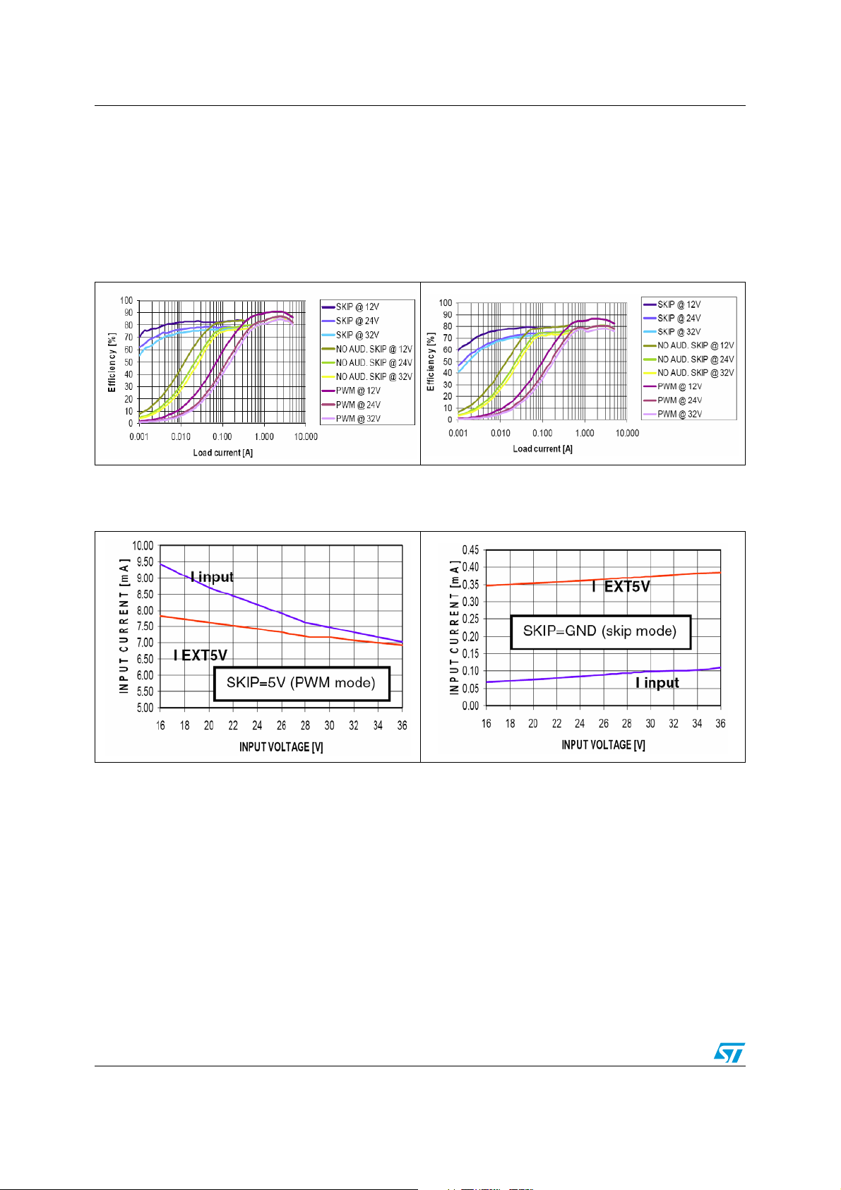
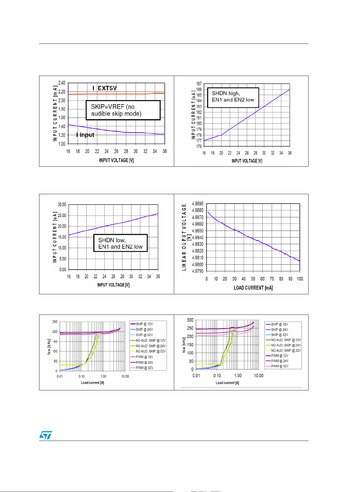
5 Typical operating characteristics
FSEL=GND(200/300 kHz), SKIP=GND(skip mode), V5SW=EXT5V (external 5 V power
supply connected), input voltage VIN = 24 V, SHDN, EN1 and EN2 high, OUT1 = 3.3 V,
OUT2 = 1.8 V, no load unless specified)
Figure 3. OUT1 = 3.3 V efficiency Figure 4. OUT2 = 1.8 V efficiency
Figure 5. PWM no load battery current vs
input voltage
Figure 6. Skip no load battery current vs
input voltage
12/48
Page 13
PM6680A Typical operating characteristics
Figure 7. No-audible skip no load battery
current vs input voltage
Figure 9. Shutdown mode input battery
current vs input voltage
Figure 8. Standby mode input battery current
vs input voltage
Figure 10. LDO5 vs output current
Figure 11. OUT1 = 3.3 V switching frequency Figure 12. OUT2 = 1.8 V switching frequency
13/48
Page 14

Typical operating characteristics PM6680A
Figure 13. OUT1 = 3.3 V load regulation Figure 14. OUT2 = 1.8 V load regulation
Figure 15. Voltage reference vs load current Figure 16. OUT1, OUT2 and LDO5 Power-Up
Figure 17. OUT1 = 3.3V load transient 0→2A Figure 18. OUT2 = 1.8V load transient 0→2A
14/48
Page 15

PM6680A Typical operating characteristics
Figure 19. 3.3 V soft start (1Ω load) Figure 20. 1.8 V soft start (0.6Ω load)
Figure 21. OUT1 = 3.3 V soft end (no load) Figure 22. OUT2 = 1.8 V soft end (no load)
Figure 23. OUT1 = 3.3 V soft end (0.8 load) Figure 24. OUT2 = 1.8 V soft end (0.6 load)
15/48
Page 16

Typical operating characteristics PM6680A
Figure 25. 3.3 V no-audible skip mode Figure 26. 1.8 V no-audible skip mode
16/48
Page 17

PM6680A Application schematic
6 Application schematic
Figure 27. Simplified application schematic
J10
C17
12
S12
6
NC
PGOOD126PGOOD227SHDN
R12
V+
C16
PGND
PGND
R29
R30
SGND
12
S13
FB1
28
7
FB1
FB2
5
R13
J6
V+
C18
VIN
R28
+
PGOOD1J7PGOOD2
SGND
LDO_ADJ
R31
R32
R33
SGND
C28
SGND
1
S1
2
C27
1uF
LDO_FB
SGND
FSEL
3
SKIP
24
VREF
32
EN1
25
EN2
4
SGND
R17
FB1
R27
SGND
V+
SGND
3
R15V+R14
V+
R16C23
SGND
S3
4
31
2
4
31
2
5
6
7
8
S2
SGNDSGND
SGND
S10
SGND
SGND
CREF
4
3
2
1
SGND
J11
EXT5V
4
31
2
V5SW
OUT1+
SGND
S11
J1
OUT2+
J9
OUT2-
S8
3
2
+VIN
-VIN
J5
J2
VIN
R26
J3
LDO5V+
V+
D1
PGND
CIN
+
PGND
R5
C13
C2
C1
C26
+
C19
RLD5V
C21
+
C20
R9
BOOT2
BOOT1
V+
VIN
R3
PGND
PGND
8
7
6
51
SGND
SGND
BOOT2
R11
SGND
SGND
U1
19
SGND
18
V+
31
C22
SGND
R10
C6
BOOT1
51
6
7
C4
C3
8
PGND
PGND
R4
R6
C14
1
C8
+
C7
L1
R20
L2
1 2
3
2
HGATE210PHASE2
PM6680A
2
3
1 2
R18
M3
8
7
6
51
4
R21
13
11
LGATE2
LGATE1
15
R23
4
51
6
7
8
M4
S9
3
1
OUT1+
+
C24
C9
D3
3
2
R7
12
CSENSE2
R8
2
3
C10
R19
D2
C12
+
C11
+
C25
2
S4
M1
4
C5
9
BOOT2
VIN
LDO5
VCC
BOOT123HGATE122PHASE121CSENSE120V5SW17OUT129COMP1
R22
4
M2
S5
OUT1+
J4
PGND
PGND14SGND
V5SW
R25
PGND
C15
SGND
2
8
1
OUT2
COMP2
SGND
30
16
OUT1
LDO_FB
R24
PGND
J8
OUT1-
17/48
Page 18

Device description PM6680A
7 Device description
The PM6680A is a dual step-down controller dedicated to provide logic voltages for
industrial automation applications.
It is based on a Constant On Time control architecture. This type of control offers a very fast
load transient response with a minimum external component count. A typical application
circuit is shown in Figure 3.
The PM6680A regulates two adjustable output voltages: OUT1 and OUT2. The switching
frequency of the two sections can be adjusted to 200/300 kHz, 300/400 kHz or 400/500 kHz
respectively. In order to maximize the efficiency at light load condition, a pulse skipping
mode can be selected.
The PM6680A includes also a 5 V linear regulator (LDO5) that can power the switching
drivers. If the output OUT1 regulates 5 V, in order to maximize the efficiency in higher
consumption status, the linear regulator can be turned off and their outputs can be supplied
directly from the switching outputs. The PM6680A provides protection versus overvoltage,
undervoltage and over temperature as well as power good signals for monitoring purposes.
An external 1.237 V reference is available.
7.1 Constant on time PWM control
If the SKIP pin is tied to 5 V, the device works in PWM mode. Each power section has an
independent on time control.The PM6680A employees a pseudo-fixed switching frequency,
Constant On Time (COT) controller as core of the switched mode section. Each power
section has an independent COT control.
The COT controller is based on a relatively simple algorithm and uses the ripple voltage due
to the output capacitor's ESR to trigger the fixed on-time one-shot generator. In this way, the
output capacitor's ESR acts as a current sense resistor providing the appropriate ramp
signal to the PWM comparator. On-time one-shot duration is directly proportional to the
output voltage, sensed at the OUT1/OUT2 pins, and inversely proportional to the input
voltage, sensed at the VIN pin, as follows:
Equation 1
T
K
ON
This leads to a nearly constant switching frequency, regardless of input and output voltages.
When the output voltage goes lower than the regulated voltage Vreg, the on-time one shot
generator directly drives the high side MOSFET for a fixed on time allowing the inductor
current to increase; after the on time, an off time phase, in which the low side MOSFET is
turned on, follows. Figure 28 shows the inductor current and the output voltage waveforms
in PWM mode.
V
--------------
⋅=
OUT
V
IN
18/48
Page 19

PM6680A Device description
Figure 28. Constant ON time PWM control
The duty cycle of the buck converter in steady state is:
Equation 2
V
OUT
D
--------------=
V
IN
The PWM control works at a nearly fixed frequency f
SW
:
Equation 3
V
OUT
--------------
V
IN
------------------------------ -
f
SW
V
--------------
K
×
on
OUT
V
IN
1K⁄
==
on
As mentioned the steady state switching frequency is theoretically independent from input
voltage and from output voltage.
Actually the frequency depends on parasitic voltage drops that are present during the
charging path(high side switch resistance, inductor resistance(DCR)) and discharging
path(low side switch resistance, DCR).
As a result the switching frequency increases as a function of the load current.
Standard switching frequency values can be selected for both sections by pin FSEL as
shown in the following table:
Table 6. FSEL pin selection: typical switching frequency
Fsw@OUT1 = 3.3 V (kHz) Fsw@OUT2 = 1.8 V (kHz)
FSEL = GND 195 335
FSEL = VREF 295 440
FSEL = LDO5 390 600
19/48
Page 20

Device description PM6680A
7.2 Constant on time architecture
Figure 29 shows the simplified block diagram of a constant on time controller. A minimum
off-time constrain (350 ns typ.) is introduced to allow inductor valley current sensing on
synchronous switch. A minimum on-time (130 ns) is also introduced to assure the start-up
switching sequence.
PM6680A has a one-shot generator for each power section that turns on the high side
MOSFET when the following conditions are satisfied simultaneously: the PWM comparator
is high, the synchronous rectifier current is below the current limit threshold, and the
minimum off-time has timed out.
Once the on-time has timed out, the high side switch is turned off, while the synchronous
switch is turned on according to the anti-cross conduction circuitry management.
When the negative input voltage at the PWM comparator (Figure 29), which is a scaleddown replica of the output voltage (see the external R1/R2 divider in Figure 29), reaches the
valley limit (determined by internal reference Vr = 0.9 V), the low-side MOSFET is turned off
according to the anti-cross conduction logic once again, and a new cycle begins.
Figure 29. Constant on-time block diagram
In steady state the FB pin voltage is about Vr and the regulated output voltage depends on
the external divider:
Equation 4
OUT Vr 1
20/48
R
2
⎛⎞
------ -+
×=
⎝⎠
R
1
Page 21

PM6680A Device description
7.3 Output ripple compensation and loop stability
In a classic constant on time control, the system regulates the valley value of the output
voltage and not the average value, as shown in Figure 28 In this condition, the output
voltage ripple is source of a DC static error.
To compensate this error, an integrator network can be introduced in the control loop, by
connecting the output voltage to the COMP1/COMP2 (for the OUT1 and OUT2 sections
respectively) pin through a capacitor C
as in Figure 30.
INT
Figure 30.
Circuitry for output ripple compensation
The integrator amplifier generates a current, proportional to the DC errors between the FB
voltage and Vr, which decreases the output voltage in order to compensate the total static
error, including the voltage drop on PCB traces. In addition, C
provides an AC path for the
INT
output ripple. In steady state, the voltage on COMP1/COMP2 pin is the sum of the reference
voltage Vr and the output ripple (see Figure 30). In fact when the voltage on the COMP pin
reaches Vr, a fixed Ton begins and the output increases.
For example, we consider Vout = 5 V with an output ripple of ∆V = 50 mV. Considering C
>> C
FILT
, the C
DC voltage drop VC
INT
is about 5 V -Vr + 25 mV = 4.125 V. C
INT
INT
INT
assures
an AC path for the output voltage ripple. Then the COMP pin ripple is a replica of the output
ripple, with a DC value of Vr + 25 mV = 925 mV.
For more details about the output ripple compensation network, see the Chapter 9.6:
Closing the integrator loop on page 35 in the Design guidelines.
21/48
Page 22

Device description PM6680A
7.4 Pulse skip mode
If the SKIP pin is tied to ground, the device works in skip mode.
At light loads a zero-crossing comparator truncates the low-side switch on-time when the
inductor current becomes negative. In this condition the section works in discontinuous
conduction mode. The threshold between continuous and discontinuous conduction mode
is:
Equation 5
–
V
INVOUT
ILOAD SKIP()
For higher loads the inductor current doesn’t cross the zero and the device works in the
same way as in PWM mode and the frequency is fixed to the nominal value.
----------------------------- -
2L×
×=
T
ON
Figure 31.
PWM and pulse skip mode inductor current
Figure 31 shows inductor current waveforms in PWM and SKIP mode. In order to keep
average inductor current equal to load current, in SKIP mode some switching cycles are
skipped. When the output ripple reaches the regulated voltage Vreg, a new cycle begins.
The off cycle duration and the switching frequency depend on the load condition.
As a result of the control technique, losses are reduced at light loads, improving the system
efficiency.
22/48
Page 23
PM6680A Device description
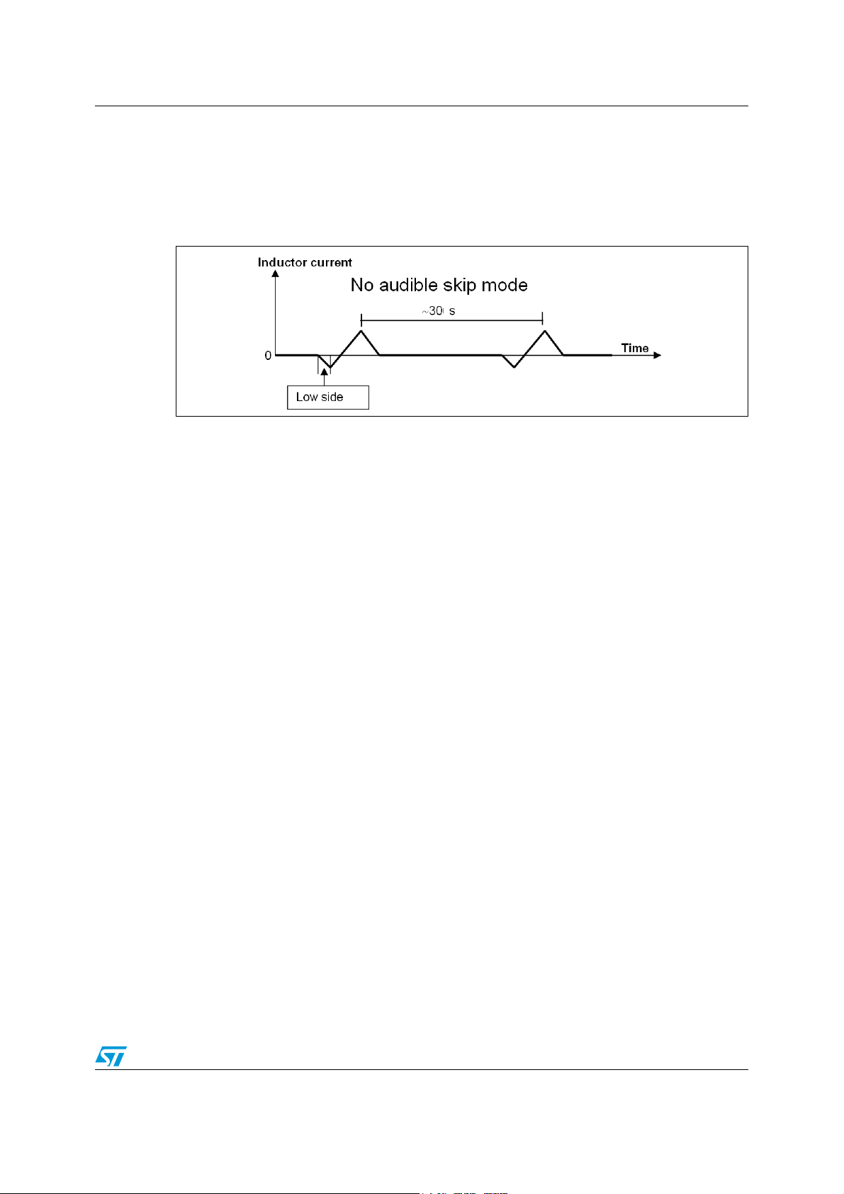
7.5 No-audible skip mode
If SKIP pin is tied to V
33 kHz is enabled. At light load condition, If there is not a new switching cycle within a 30 µs
(typ.) period, a no-audible skip mode cycle begins.
Figure 32. No audible skip mode
The low side switch is turned on until the output voltage crosses about Vreg + 1 %. Then the
high side MOSFET is turned on for a fixed on time period. Afterwards the low side switch is
enabled until the inductor current reaches the zero-crossing threshold. This keeps the
switching frequency higher than 33 kHz. As a consequence of the control, the regulated
voltage can be slightly higher than Vreg (up to 1 % ).
If, due to the load, the frequency is higher than 33 kHz, the device works like in skip mode.
No-audible skip mode reduces audio frequency noise that may occur in pulse skip mode at
very light loads, keeping the efficiency higher than in PWM mode.
, a no-audible skip mode with a minimum switching frequency of
REF
µ
23/48
Page 24
Device description PM6680A
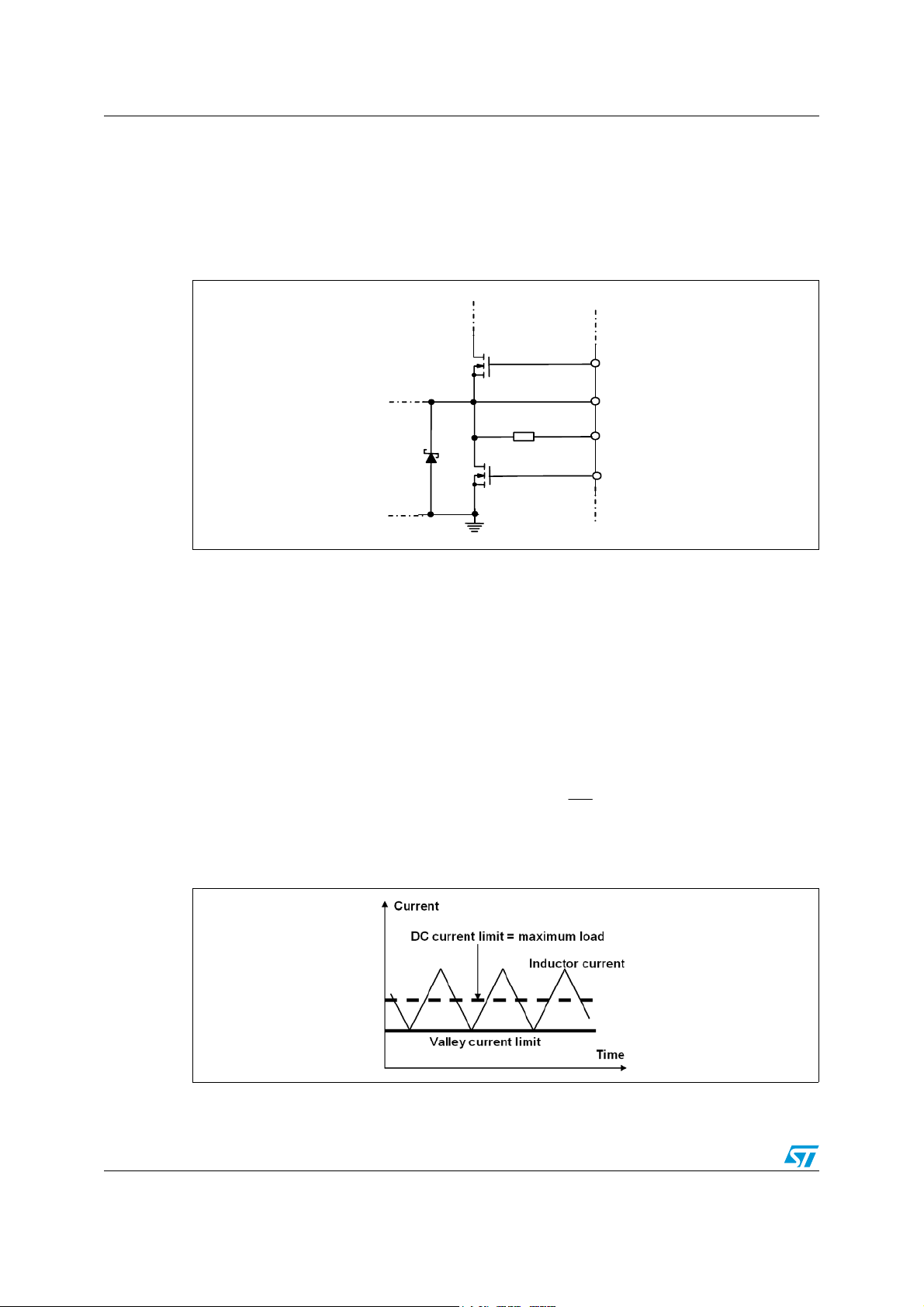
7.6 Current limit
The current-limit circuit employs a "valley" current-sensing algorithm. During the conduction
time of the low side MOSFET the current flowing through it is sensed. The current-sensing
element is the low side MOSFET on-resistance (Figure 33).
Figure 33. Rsense sensing technique
HS
Rcsense
LS
RDS
HGATE
PHASE
CSENSE
LGATE
on
An internal 100 µA current source is connected to CSENSE pin and determines a voltage
drop on RCSENSE. If the voltage across the sensing element is greater than this voltage
drop, the controller doesn't initiate a new cycle. A new cycle starts only when the sensed
current goes below the current limit.
Since the current limit circuit is a valley current limit, the actual peak current limit is greater
than the current limit threshold by an amount equal to the inductor ripple current.
Moreover the maximum DC load is equal to the valley current limit plus half of the inductor
ripple current:
Equation 6
∆
I
L
+=
I(max)I
LvalleyLOAD
2
The output current limit depends on the current ripple, as shown in Figure 34:
Figure 34. Current waveforms in current limit conditions
24/48
Page 25

PM6680A Device description
Being fixed the valley threshold, the greater the current ripple is, greater the DC output
current is The valley current limit can be set with resistor RCSENSE:
Equation 7
R
CSENSE
R
---------------------------------------------=
×
DS on()ILvalley
Icsense
Where I
CSENSE
= 100 µA, RDSon is the drain-source on resistance of the low side switch.
Consider the temperature effect and the worst case value in RDSon calculation.
The accuracy of the valley current threshold detection depends on the offset of the internal
comparator (∆V
) and on the accuracy of the current generator (∆I
OFF
CSENSE
)
Equation 8
∆
I
I
Lvalley
Lvalley
⎡
∆
I
CSENSE
=
I
CSENSE
+
∆
V
⎢
⎣
OFF
×
IR
CSENSECSENSE
×
100
⎤
R
∆
CSENSE
+
⎥
R
CSENSE
⎦
R
∆
SNS
+
R
SNS
Where RSNS is the sensing element(RDSon)
PM6680A provides also a fixed negative peak current limit to prevent an excessive reverse
inductor current when the switching section sinks current from the load in PWM mode. This
negative current limit threshold is measured between PHASE and SGND pins, comparing
the magnitude drop on the PHASE node during the conduction time of the low side
MOSFET with an internal fixed voltage of 120 mV.
The negative valley-current limit I
(if the device works in PWM mode) is given by:
NEG
Equation 9
mV
NEG
=
120
R
DSon
I
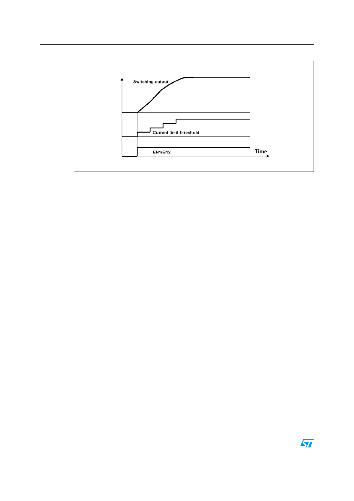
7.7 Soft start and soft end
Each switching section is enabled separately by asserting high EN1/EN2 pins respectively.
In order to realize the soft start, at the startup the overcurrent threshold is set 25 % of the
nominal value and the undervoltage protection (see related sections) is disabled. The
controller starts charging the output capacitor working in current limit. The overcurrent
threshold is increased from 25 % to 100 % of the nominal value with steps of 25 % every
700 µs (typ.). After 2.8 ms (typ.) the undervoltage protection is enabled. The soft start time is
not programmable. A minimum capacitor C
overshoot on the output:
Equation 10
is required to ensure a soft start without any
INT
A6
C ×
≥
INT
µ
I
Lvalley
+
4
25/48
C
out
I
∆
L
2
Page 26
Device description PM6680A
Figure 35. Soft start waveforms
When a switching section is turned off (EN1/EN2 pins low), the controller enters in soft end
mode.The output capacitor is discharged through an internal 18 Ω p-MOSFET switch; when
the output voltage reaches 0.3 V, the low-side MOSFET turns on, keeping the output to
ground. The soft end time also depends on load condition.
7.8 Gate drivers
The integrated high-current drivers allow to use different power MOSFETs. The high side
driver MOSFET uses a bootstrap circuit which is indirectly supplied by LDO5 output. The
BOOT and PHASE pins work respectively as supply and return rails for the HS driver.
The low side driver uses the internal LDO5 output for the supply rail and PGND pin as return
rail.
An important feature of the gate drivers is the adaptive anti-cross conduction protection,
which prevents high side and low side MOSFETs from being on at the same time. When the
high side MOSFET is turned off the voltage at the phase node begins to fall. The low side
MOSFET is turned on when the voltage at the phase node reaches an internal threshold.
When the low side MOSFET is turned off, the high side remains off until the LGATE pin
voltage goes approximatively under 1 V.
The power dissipation of the drivers is a function of the total gate charge of the external
power MOSFETs and the switching frequency, as shown in the following equation:
Equation 11
Where V
is the 5 V driver supply.
driver
P
driverVdriverQg
× fSW×=
26/48
Page 27

PM6680A Device description
7.9 Reference voltage and bandgap
The 1.237 V (typ.) internal bandgap voltage is accurate to ±1 % over the temperature range.
It is externally available (VREF pin) and can supply up to ± 100 µA and can be used as a
voltage threshold for the multifunction pins FSEL and SKIP to select the appropriate working
mode. Bypass VREF to ground with a 100 nF minimum capacitor.
If VREF goes below 0.87 V (typ.) , the system detects a fault condition and all the circuitry is
turned off. A toggle on the input voltage (power on reset) or a toggle on SHDN pin is
necessary to restart the device.
An internal divider of the bandgap provides a voltage reference Vr of 0.9 V. This voltage is
used as reference for the linear and the switching regulators outputs. The overvoltage
protection, the undervoltage protection and the power good signals are referred to Vr.
7.10 Internal linear regulator
The PM6680A has an internal linear regulator providing 5 V (LDO5) at ± 2 % accuracy. High
side drivers, low side drivers and most of internal circuitry are supplied by LDO5 output
through VCC pin (an external RC filter may be applied between LDO5 and VCC). The linear
regulator can provide an average output current of 50 mA and a peak output current of 100
mA. Bypass LDO5 output with a minimum 1µF ceramic capacitor and a 4,7 µF tantalum
capacitor ( ESR
and all the circuitry is turned off. A power on reset or a toggle on SHDN pin is necessary to
restart the device.
≥ 2 Ω). If the 5 V output goes below 4 V, the system detects a fault condition
V5SW pin allows to keep the 5 V linear regulator always active or to enable the internal
bootstrap-switchover function: if the 5 V switching output is connected to V5SW, when the
voltage on V5SW pin is above 4.8 V, an internal 3.0
Ω max p-channel MOSFET switch
connects V5SW pin to LDO5 pin and simultaneously LDO5 shuts down. This configuration
allows to achieve higher efficiency. V5SW can be connected also to an external 5 V supply.
LDO5 regulator turns off and LDO5 is supplied externally. If V5SW is connected to ground,
the internal 5 V regulator is always on and supplies LDO5 output
Table 7. V5SW multifunction pin
V5SW Description
GND The 5 V linear regulator is always turned on and supplies LDO5 output.
Switching 5 V
output
External 5 V
supply
The 5 V linear regulator is turned off when the voltage on V5SW is above 4.8 V and
the LDO5 output is supplied by the switching 5 V output.
The 5 V linear regulator is turned off when the voltage on V5SW is above 4.8 V and
LDO5 output is supplied by the external 5 V.
27/48
Page 28

Device description PM6680A
7.11 Power up sequencing and operative modes
Let us consider SHDN, EN1 and EN2 low at the beginning. An external voltage is applied as
input voltage. The device is in shutdown mode.
When the SHDN pin voltage is above the shutdown device on threshold (1.5 V typ.), the
controller begins the power-up sequence. All the latched faults are cleared. LDO5
undervoltage control is blanked for 4 ms and the internal regulator LDO5 turns on. If the
LDO5 output is above the UVLO threshold after this time, the device enters in standby
mode. The switching outputs are kept to ground by turning on the low side MOSFETs.
When EN1 and EN2 pins are forced high the switching sections begin their soft start
sequence.
Table 8. Operatives modes
Mode Conditions Description
Run
Standby
Shutdown SHDN is low All circuits off.
SHDN is high,
EN1/EN2 pins are high
Both EN1/EN2 pins are low
and SHDN pin is high
Switching regulators are enabled; internal linear
regulators outputs are enabled.
Internal Linear regulators active (LDO5 is always on).
In Standby mode LGATE1/LGATE2 pins are forced
high while HGATE1/HGATE2 pins are forced low.
28/48
Page 29
PM6680A Monitoring and protections
8 Monitoring and protections
Power good signals
The PM6680A provides two independent power good signals: one for each switching
section (PGOOD1/PGOOD2).
PGOOD1/PGOOD2 signals are low if the output voltage is out of ± 10 % of the designed set
point or during the soft-start, standby and shutdown mode.
Thermal protection
The PM6680A has a thermal protection to preserve the device from overheating. The
thermal shutdown occurs when the die temperature goes above +150 °C. In this case all
internal circutry is turned off and the power sections are turned off after the discharge mode.
A power on reset or a toggle on the SHDN pin is necessary to restart the device.
Overvoltage protection
When the switching output voltage is about 115 % of its nominal value, a latched
overvoltage protection occurs. In this case, the synchronous rectifier immediately turns on
while the high-side MOSFET turns off. The output capacitor is rapidly discharged and the
load is preserved from being damaged. The overvoltge protection is also active during the
soft start. Once an overvoltage protection has been detected, a toggle on SHDN, EN1/EN2
pins or a power on reset is necessary to exit from the latched state.
Undervoltage protection
When the switching output voltage is below 70 % of its nominal value, a latched
undervoltage protection occurs. In this case the switching section is immediately disabled
and both switches are open. The controller enters in soft end mode and the output is
eventually kept to ground, turning low side MOSFET on. The undervoltage circuit protection
is enabled only at the end of the soft-start. Once an overvoltage protection has been
detected, a toggle on SHDN, EN1/EN2 pin or a power on reset is necessary to clear the
undervoltage fault and starts with a new soft-start phase.
Table 9. Protections and operatives modes
Mode Conditions Description
Overvoltage
protection
Undervoltage
protection
Thermal
shutdown
OUT1/OUT2 > 115% of the
nominal value
OUT1/OUT2 < 70 % of the
nominal value
> +150 °C
T
J
LGATE1/LGATE2 pin is forced high, LDO5 remains
active. Exit by a power on reset or toggling SHDN or
EN1/EN2
LGATE1/LGATE2 is forced high after the soft end
mode, LDO5 remains active. Exit by a power on reset
or toggling SHDN or EN1/EN2
All circuitry off. Exit by a POR on VIN or toggling
SHDN.
29/48
Page 30

Design guidelines PM6680A
9 Design guidelines
The design of a switching section starts from two parameters:
● Input voltage range: in notebook applications it varies from the minimum battery
voltage, VINmin to the AC adapter voltage, V
● Maximum load current: it is the maximum required output current, I
9.1 Switching frequency
It's possible to set 3 different working frequency ranges for the two sections with FSEL pin
(
Ta bl e 6 ).
Switching frequency mainly influences two parameters:
● Inductor size: for a given saturation current and RMS current, greater frequency allows
to use lower inductor values, which means smaller size.
● Efficiency: switching losses are proportional to frequency. High frequency generally
involves low efficiency.
INmax
.
LOAD(max)
.
9.2 Inductor selection
Once that switching frequency is defined, inductor selection depends on the desired
inductor ripple current and load transient performance.
Low inductance means great ripple current and could generate great output noise. On the
other hand, low inductor values involve fast load transient response.
A good compromise between the transient response time, the efficiency, the cost and the
size is to choose the inductor value in order to maintain the inductor ripple current ∆I
between 20 % and 50 % of the maximum output current I
occurs at the maximum input voltage. With this considerations, the inductor value can be
calculated with the following relationship:
Equation 12
where fsw is the switching frequency, VIN is the input voltage, V
∆I
is the selected inductor ripple current.
L
In order to prevent overtemperature working conditions, inductor must be able to provide an
RMS current greater than the maximum RMS inductor current I
Equation 13
VV
−
L ×
=
OUTIN
If
∆×
Lsw
V
OUT
V
LOAD(max)
IN
. The maximum ∆IL
is the output voltage and
OUT
:
LRMS
L
LOADLRMS
Where ∆I
30/48
is the maximum ripple current:
L(max)
(max))I(
2
12
∆
2
L
(max))I(I
+=
Page 31

PM6680A Design guidelines
∆×=
Equation 14
VV
sw
−
Lf
×
(max)I ×
L
=∆
V
OUTmaxIN
OUT
V
maxIN
If hard saturation inductors are used, the inductor saturation current should be much greater
than the maximum inductor peak current Ipeak:
Equation 15
(max)I
∆
LOAD
(max)IIpeak
L
+=
2
Using soft saturation inductors it's possible to choose inductors with saturation current limit
nearly to Ipeak.
Below there is a list of some inductor manufacturers.
Table 10. Inductor manufacturer
Manufacturer Series
COILCRAFT MSS1038 1.5 to 22 2.85 to 7.85 2.9 to 8.30
COILCRAFT MSS7341 3.3 to 22 1.7 to 3.95 1.3 to 3.5
Inductor value
(uH)
RMS current
(A)
Saturation current
(A)
WURTH TPC 1 to 22 µH 2.7 to 8 2.6 to 9.5
9.3 Output capacitor
The selection of the output capacitor is based on the ESR value Rout and the voltage rating
rather than on the capacitor value Cout.
The output capacitor has to satisfy the output voltage ripple requirements. Lower inductor
value can reduce the size of the choke but increases the inductor current ripple ∆IL.
Since the voltage ripple V
Equation 16
A low ESR capacitor is required to reduce the output voltage ripple. Switching sections can
work correctly even with 20 mV output ripple.
However, to reduce jitter noise between the two switching sections it's preferable to work
with an output voltage ripple greater than 30 mV. If lower output ripple is required, a further
compensation network is needed (see Closing the integrator loop paragraph).
Finally the output capacitor choice deeply impacts on the load transient response (see Load
transient response paragraph). Below there is a list of some capacitor manufacturers.
RIPPLEout
is given by:
IRV
LoutRIPPLEout
31/48
Page 32

Design guidelines PM6680A
Table 11. Output capacitor manufacturer
Manufacturer Series
SANYO
PANASONIC SPCAP UD, UE 100 to 470 2 to 6.3 7 to 18
POSCAP TPB, TPD,
TPE
9.4 Input capacitors selection
In a buck topology converter the current that flows into the input capacitor is a pulsed current
with zero average value. The input RMS current of the two switching sections can be roughly
estimated as follows:
Equation 17
Where D1, D2 are the duty cycles and I1, I2 are the maximum load currents of the two
sections.
Input capacitor should be chosen with an RMS rated current higher than the maximum RMS
current given by both sections.
Capacitor value
(uF)
100 to 470 2.5 to 6.3 12 to 65
2
11CinRMS
Rated voltage (V) ESR max (mΩ)
2
221
)D1(ID)D1(IDI
−××+−××=
2
Tantalum capacitors are good in term of low ESR and small size, but they occasionally can
burn out if subjected to very high current during the charge. Ceramic capacitors have
usually a higher RMS current rating with smaller size and they remain the best choice.
Below there is a list of some ceramic capacitor manufacturers.
Table 12. Input capacitor manufacturer
Manufacturer Series Capacitor value (uF) Rated voltage (V)
TAYIO YUDEN UMK325BJ106KM-T 10 50
TAYIO YUDEN GMK325BJ106MN 10 35
32/48
Page 33

PM6680A Design guidelines
=
9.5 Power MOSFETS
Logic-level MOSFETs are recommended, since low side and high side gate drivers are
powered by LDO5. Their breakdown voltage VBR
must be higher than V
DSS
In notebook applications, power management efficiency is a high level requirement. The
power dissipation on the power switches becomes an important factor in switching
selections. Losses of high-side and low-side MOSFETs depend on their working conditions.
The power dissipation of the high-side MOSFET is given by:
Equation 18
PPP +=
switchingconductionDHighSide
Maximum conduction losses are approximately:
Equation 19
INmax
.
V
RP ××=
DSonconduction
OUT
V
LOAD
minIN
2
(max)I
where RDSon is the drain-source on resistance of the high side MOSFET.
Switching losses are approximately:
Equation 20
∆
I
L
+×
2
××
ft)
swoff
2
phases of the MOSFET.
P
switching
where ton and t
∆
I
=
LOADIN
are the switching times of the turn on and turn
off
2
2
L
−×
(max)I(V
××
ft)
+
(max)I(V
LOADINswon
off
As general rule, high side MOSFETs with low gate charge are recommended, in order to
minimize driver losses.
Below there is a list of possible choices for the high side MOSFET.
Table 13. High side MOSFET manufacturer
Manufacturer Type Gate charge (nC) Rated reverse voltage (V)
ST STS5NF60L 25 60
The power dissipation of the low side MOSFET is given by:
Equation 21
PP
conductionDLowSide
Maximum conduction losses occur at the maximum input voltage:
33/48
Page 34

Design guidelines PM6680A
Equation 22
DSonconduction
Choose a synchronous rectifier with low R
⎛
⎜
1RP ×
−×=
⎜
⎝
. When high side MOSFET turns on, the fast
DSon
⎞
V
OUT
⎟
LOAD
⎟
V
maxIN
⎠
2
(max)I
variation of the phase node voltage can bring up even the low side gate through its gatedrain capacitance C
that minimizes the ratio C
, causing cross-conduction problems. Choose a low side MOSFET
RSS
RSS/CGS
(C
GS
= C
ISS
- C
RSS
).
Below there is a list of some possible low side MOSFETs.
Table 10. Low side MOSFET manufacturer
C
RSS
Manufacturer Type R
ST STS7NF60L [VC11] 19 0.0625 60
DSon
(mΩ)
--------------
C
GS
Rated reverse voltage
(V)
Dual n-channel MOSFETs can be used in applications with a maximum output current of
about 3 A. Below there is a list of some MOSFET manufacturers.
Table 14. Dual MOSFET manufacturer
Manufacturer Type R
ST STS4DNF60L 50 15 60
DSon
(mΩ)
Gate charge
(nC)
Rated reverse voltage
(V)
A rectifier across the low side MOSFET is recommended. The rectifier works as a voltage
clamp across the synchronous rectifier and reduces the negative inductor swing during the
dead time between turning the high-side MOSFET off and the synchronous rectifier on. It
can increase the efficiency of the switching section, since it reduces the low side switch
losses. A shottky diode is suitable for its low forward voltage drop (0.3 V). The diode reverse
voltage must be greater than the maximum input voltage V
. A minimum recovery
INmax
reverse charge is preferable. Below there is a list of some shottky diode manufacturers.
Table 15. Schottky diode manufacturer
Manufacturer Series
ST STPS1L40M 0.5 40 21
Forward voltage
(V)
Rated reverse
voltage (V)
Reverse current
(uA)
34/48
Page 35

PM6680A Design guidelines
g
g
r
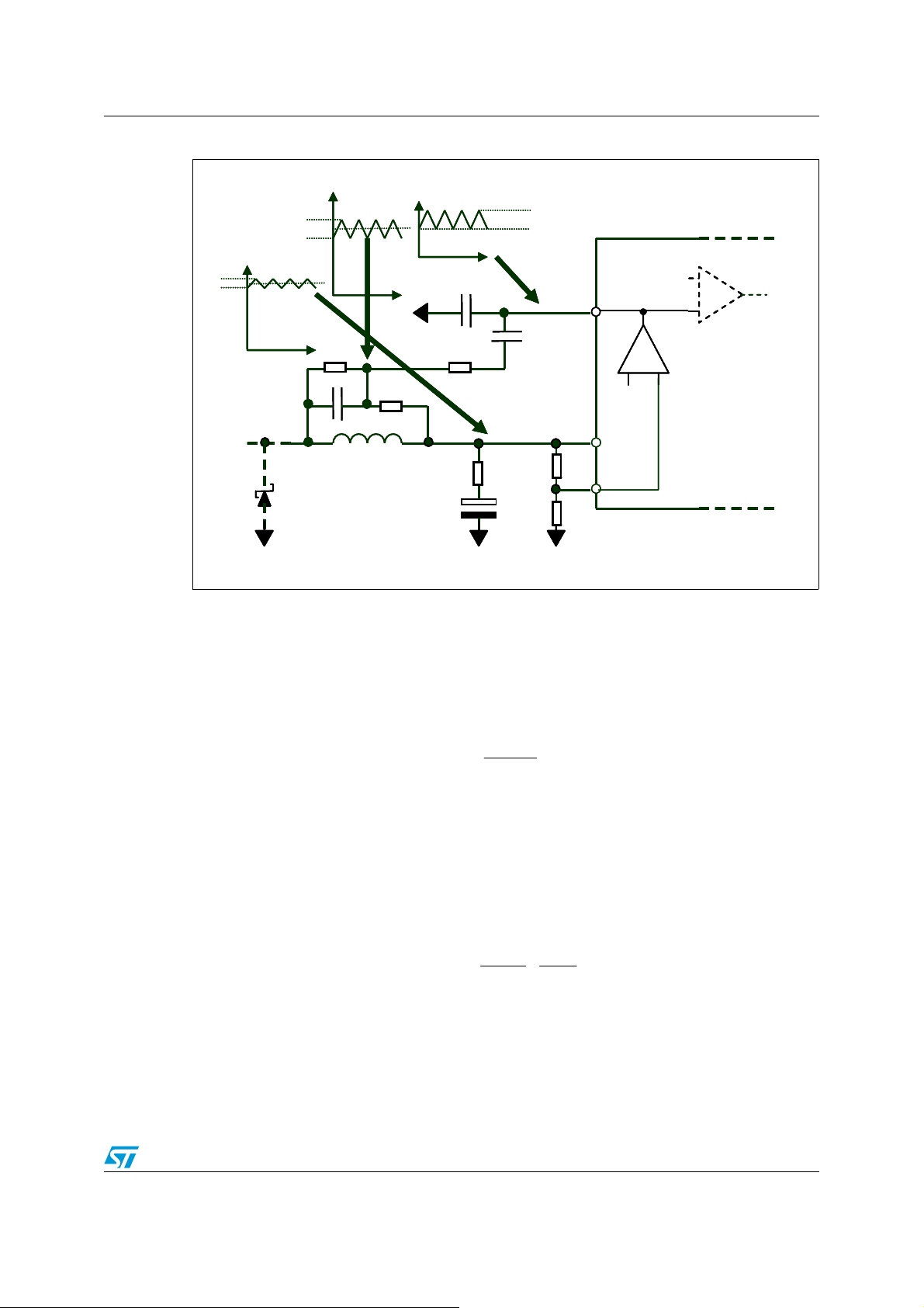
9.6 Closing the integrator loop
The design of external feedback network depends on the output voltage ripple. If the ripple
is higher than approximately 30 mV, the feedback network (
keep the loop stable.
Figure 36. Circuitry for output ripple compensation
Figure 36) is usually enough to
V
COMP PIN
VOLTAGE
∆
?V
t
D
D
∆
?V
Vr
t
T
C
FFIILLT
C
C
IINNT
C
R
IINNT
R
L
L
T
R
OOUUT
R
T
C
OOUUT
C
CCOOMMP
T
C
V
IINNT
C
V
T
OOUUT
2
R
2
R
1
R
1
R
T
P
T
B
FFB
I=gm(V1-Vr)
m
m
+
+
-
PPWWMM
CCoommppaarraattoor
OUTPUT
VOLTAGE
The stability of the system depends firstly on the output capacitor zero frequency.
The following condition should be satisfied:
r
Equation 23
fkf
=×>
Zoutsw
k
RC2
××π
outout
where k is a design parameter greater than 3 and Rout is the ESR of the output capacitor. It
determinates the minimum integrator capacitor value C
INT
:
Equation 24
g
>
C ×
INT
2
m
f
⎛
sw
−×π
f
⎜
⎜
⎝
Zout
k
Vr
V
⎞
OUT
⎟
⎟
⎠
where gm = 50 µs is the integrator transconductance.
35/48
Page 36

Design guidelines PM6680A
In order to ensure stability it must be also verified that:
Equation 25
g
C ×
INT
m
>
f2
×π
Vr
V
OUTZout
In order to reduce ground noise due to load transient on the other section, it is
recommended to add a resistor R
low pass filter (see figure 13). The cutoff frequency f
and a capacitor C
INT
that, together with C
filt
must be much greater (10 or more
CUT
, realize a
INT
times) than the switching frequency of the section:
Equation 26
f2
CUT
1
×
CC
××π
filtINT
+
CC
filtINT
Due to the capacitive divider (C
R
INT
=
INT
, C
), the ripple voltage at the COMP pin is given by:
filt
Equation 27
C
INT
×=
CC
+
RIPPLEout
filtINT
qV
×=
Where V
RIPPLEout
VV
RIPPLEoutRIPPLE
INT
is the output ripple and q is the attenuation factor of the output ripple.
If the ripple is very small (lower than approximately 30 mV), a further compensation network,
named virtual ESR network, is needed. This additional part generates a triangular ripple
that is added to the ESR output voltage ripple at the input of the integrator network. The
complete control schematic is represented in
Figure 37.
36/48
Page 37
PM6680A Design guidelines
Figure 37. Virtual ESR network
COMP pin
R
R
R
COMP pin
voltage
voltage
t
t
R
R
R
R
C
C
C
C
C
C
C
C
INT
INT
R
R
INT
INT
R
R
OUT
OUT
OUT
OUT
OUT
OUT
OUT
OUT
Vr
Vr
FILT
FILT
FILT
FILT
∆V1
∆V1
t
t
Vr
Vr
Vr
Vr
+
V1
V1
V1
V1
+
-
-
PWM
PWM
PWM
PWM
Comparator
Comparator
Comparator
Comparator
COMP
COMP
COMP
COMP
gm
gm
gm
Vr
Vr
Vr
Vr
gm
-
-+
+
C
C
INT
INT
INT
INT
C
C
OU
OU
OU
OU
T
T
T
T
2
2
2
R
R
R
2
2
2
R
R
R
FB
FB
FB
FB
1
1
1
R
R
R
1
1
1
R
R
R
∆V
∆V
Output
Output
voltage
voltage
D
D
D
D
∆V1
∆V1
t
t
T node
T node
voltage
voltage
R1
R1
R1
R1
C
CCR
C
T
T
L
L
L
L
The T node voltage is the sum of the output voltage and the triangular waveform generated
by the virtual ESR network. In fact the virtual ESR network behaves like a further equivalent
ESR.
A good trade-off is to design the network in order to achieve an R
given by:
ESR
Equation 28
V
=
RIPPLE
∆
I
L
RIPPLE
R
out
is the overall ripple of the T node
R −
ESR
where ∆IL is the inductor current ripple and V
voltage. It should be chosen higher than approximately 30 mV.
The new closed loop gain depends on C
In order to ensure stability it must be verified
INT.
that:
Equation 29
g
C ×
INT
m
>
×π
Vr
V
f2
OUTZ
Where:
37/48
Page 38

Design guidelines PM6680A
Equation 30
1
RC2
××π
TOTout
and the equivalent ESR given
out
where R
f
=
Z
is the sum of the ESR of the output capacitor R
TOT
by the virtual ESR network RESR.
Moreover C
must meet the following condition:
INT
Equation 31
fkf
=×>
Zsw
k
RC2
××π
TOTout
Where k is a free design parameter greater than 3 and determines the minimum integrator
capacitor value C
INT
:
Equation 32
g
C ×
>
INT
m
f
⎛
sw
2
−×π
⎜
⎜
k
⎝
Vr
V
⎞
OUT
f
⎟
Z
⎟
⎠
C must be selected as shown:
Equation 33
C5C×>
INT
R must be chosen in order to have enough ripple voltage on integrator input:
Equation 34
R
L
=
ESR
CR
×
R1 can be selected as follows:
Equation 35
⎛
⎜
×
R
⎜
⎝
=
1R
−
R
⎞
1
⎟
⎟
×π×
fC
Z
⎠
1
×π×
fC
Z
Example:
OUT1=1.5 V, f
We design R
R
= 1 kΩ by eq.27, 28. C = 5.6 nF by Eq.34. Then R = 36 kΩ (eq.34) and R1 = 3 kΩ
INT
= 290 kHz, L = 2.5 µH, Cout = 330 µF with Rout < 12 mΩ.
SW
= 12 mΩ. We choose C
ESR
= 1 nF by equations 30, 33 and Cfilt = 47 pF,
INT
(eq.35).
38/48
Page 39

PM6680A Design guidelines
V
V
p
p
V
V
9.7 Other parts design
● VIN filter
A VIN pin low pass filter is suggested to reduce switching noise. The low pass filter is
shown in the next figure:
Figure 38. VIN pin filter
R
R
N
Input
voltage
C
C
0
11000
Typical components values are: R = 3.9 Ω and C = 4.7 µF.
● VCC filter
A VCC low pass filter helps to reject switching commutations noise:
IIN
F
F
Figure 39. Inductor current waveforms
5
LLDDOO5
R
R
C
CCC
C
C
Typical components values are: R = 47 Ω and C = 1µF.
● VREF capacitor
A 10nF to 100nF ceramic capacitor on VREF pin must be added to ensure noise
rejection.
● LDO5 output capacitors
Bypass the output of each linear regulator with 1 µF ceramic capacitor closer to the
LDO pin and a 4.7µF tantalum capacitor (ESR = 2 Ω). In most applicative conditions a
4.7 µF ceramic output capacitor can be enough to ensure stability.
● Bootstrap circuit
The external bootstrap circuit is represented in the next figure:
39/48
Page 40

Design guidelines PM6680A
A
A
Figure 40. Bootstrap circuit
D
D
R
T
BBOOOOT
R
BBOOOOT
C
T
BBOOOOT
L
L
C
PPH
LLDDOO5
H
T
SSE
5
E
The bootstrap circuit capacitor value C
side MOSFET during turn on phase. A typical value is 100 nF.
The bootstrap diode D must charge the capacitor during the off time phases. The maximum
rated voltage must be higher than V
A resistor R
on the BOOT pin could be added in order to reduce noise when the phase
BOOT
node rises up, working like a gate resistor for the turn on phase of the high side MOSFET.
9.8 Design example
The following design example considers an input voltage from 16 V to 32 V(the typical value
is 24 V). The two switching outputs are OUT1 = 3.3 V and OUT2 = 1.8 V and must deliver a
maximum current of 2.5 A. The selected switching frequencies are about 290 kHz for OUT1
section and about 440 kHz for OUT2 section (see
1. Inductor selection
OUT1: ILOAD = 2.5 A, 45 % ripple current.
Equation 36
We choose standard value L= 8.2 µH.
BOOT
INmax
must provide the total gate charge to the high
.
Ta bl e 6 ).
∆I
I
LRMS
I
peak
= 1.16 A @VIN = 24 V.
L(max)
= 2.523 A
= 2.5 A + 0.58 A = 3.83 A
OUT2:ILOAD=2.5 A, 35 % ripple current.
40/48
Page 41

PM6680A Design guidelines
Equation 37
We choose standard value L=4.7 µH.
∆I
I
LRMS
I
peak
= 0.886 A @VIN =24 V.
L(max)
= 2.523 A
= 2.5 A + 0.58 A = 3.83 A
2. Output capacitor selection
We would like to have an output ripple smaller than 25 mV.
OUT1: POSCAP 4TPE150MI
OUT2: POSCAP 6TPE220M
3. Power MOSFETs
OUT1:High side: STS5NF60L
Low side: STS7NF60L
OUT2:High side: STS5NF60L
Low side: STS7NF60L
4. Current limit
OUT1:
Equation 38
A
Equation 39
(Let's assume the maximum temperature Tmax = 75 °C in R
choose standard value R
CSENSE
= 560 Ω.
OUT2:
Equation 40
41/48
calculation). We
DSon
Page 42

Design guidelines PM6680A
Equation 41
(Let's assume Tmax=75 °C in R
R
CSENSE
= 560 Ω.
calculation). We choose standard value
DSon
5. Input capacitor
Maximum input capacitor RMS current is about 1.084 A. Then I
CINRMS
> 1.084 A
We put two 10 µF ceramic capacitors with Irms = 1.5 A.
6. Synchronous rectifier
OUT1: Shottky diode STPS1L40M
OUT2: Shottky diode STPS1L40M
7. Integrator loop
(Refer to figure 14)
OUT1: The ripple is smaller than 40 mV, then the virtual ESR network is required.
C
= 1.5 nF; C
INT
= 47 pF; R
filt
= 1.1 kΩ
INT
OUT2: The ripple is smaller than 40 mV, then the virtual ESR network is required.
C
=1.5 nF; C
INT
=47 pF; R
filt
= 820 Ω
INT
8. Output feedback divider
(Refer to figure 6)
OUT1: R1 = 10 kΩ; R2 = 27 kΩ
OUT2: R1 = 10 kΩ; R2 = 10 kΩ
9. Layout guidelines
The layout is very important in terms of efficiency, stability and noise of the system. It is
possible to refer to the PM6680A demoboard for a complete layout example.
For good PC board layout follows these guidelines:
● Place on the top side all the power components (inductors, input and output capacitors,
MOSFETs and diodes). Refer them to a power ground plan, PGND. If possible, reserve
a layer to PGND plan. The PGND plan is the same for both the switching sections.
● AC current paths layout is very critical (seeFigure 41). The first priority is to minimize
their length. Trace the LS MOSFET connection to PGND plan as short as possible.
Place the synchronous diode D near the LS MOSFET. Connect the LS MOSFET drain
to the switching node with a short trace.
● Place input capacitors near HS MOSFET drain. It is recommended to use the same
input voltage plan for both the switching sections, in order to put together all input
capacitors.
● Place all the sensitive analog signals (feedbacks, voltage reference, current sense
paths) on the bottom side of the board or in an inner layer. Isolate them from the power
top side with a signal ground layer, SGND. Connect the SGND and PGND plans only in
one point (a multiple vias connection is preferable to a 0 ohm resistor connection) near
the PGND device pin. Place the device on the top or on the bottom size and connect
the exposed pad and the SGND pins to the SGND plan (see
Figure 41).
42/48
Page 43
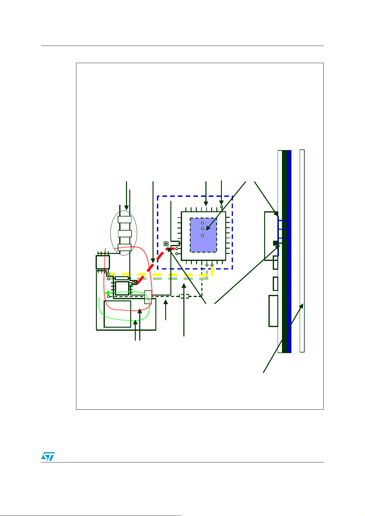
PM6680A Design guidelines
Figure 41. Current paths, ground connection and driver traces layout
SGND connection to SGND
plan
SGND connection to SGND
Device (top layer)
(inner layer)
(inner layer)
Device (top layer)
Low side gate trace (bottom layer)
Place input capacitors together
Place input capacitors together
Low side gate trace (bottom layer)
SGND plan
SGND plan
plan
Exposed pad connection to SGND
Exposed pad connection to SGND
HS
HS
Phase
Phase
SGND1
SGND1
SGND1
SGND1
PGND
PGND
PGND
IN
IN
C
C
PGND plan (top layer)
PGND plan (top layer)
D
D
LS
LS
+C
+C
OUT
L
L
OUT
Reduce the AC current
paths
Reduce the AC current
paths
PGND
LGATE1
LGATE1
LGATE5
LGATE5
SGND2
SGND2
SGND2
SGND2
CSENSE1
PHASE1
HGATE 1
CSENSE1
PHASE1
HGATE 1
CSENSE5
PHASE5
HGATE 5
CSENSE5
PHASE5
HGATE 5
Very close HGATE and PHASE
traces (inner or bottom layers)
Very close HGATE and PHASE
CSENSE dedicated trace (bottom
CSENSE dedicated trace (bottom
traces (inner or bottom layers)
layer)
layer)
Multiple vias between SGND plan and PGND
plan
Multiple vias between SGND plan and PGND
plan
PM6680
PM6680
Signal traces
Signal traces
PGND
PGND
HS
HS
LS
LS
L
L
Top layer
Top layer
PGND plan
PGND plan
SGND plan
SGND plan
Bottom layer
Bottom layer
43/48
Page 44

Design guidelines PM6680A
● As general rule, make the high side and low side drivers traces wide and short. The
high side driver is powered by the bootstrap circuit. It's very important to place
capacitor CBOOT and diode DBOOT as near as possible to the HGATE pin (for
example on the layer opposite to the device). Route HGATE and PHASE traces as near
as possible in order to minimize the area between them.
● The Low side gate driver is powered by the 5 V linear regulator output. Placing PGND
and LGATE pins near the low side MOSFETs reduces the length of the traces and the
crosstalk noise between the two sections.
● The linear regulator output LDO5 is referred to SGND as long as the reference voltage
Vref. Place their output filtering capacitors as near as possible to the device.
● Place input filtering capacitors near VCC and VIN pins.
● It would be better if the feedback networks connected to COMP, FB and OUT pins are
"referred" to SGND in the same point as reference voltage Vref. To avoid capacitive
coupling place these traces as far as possible from the gate drivers and phase
(switching) paths.
● Place the current sense traces on the bottom side. Using It is recommended to use a
dedicated connection between the switching node and the current limit resistor
R
CSENSE
.
44/48
Page 45

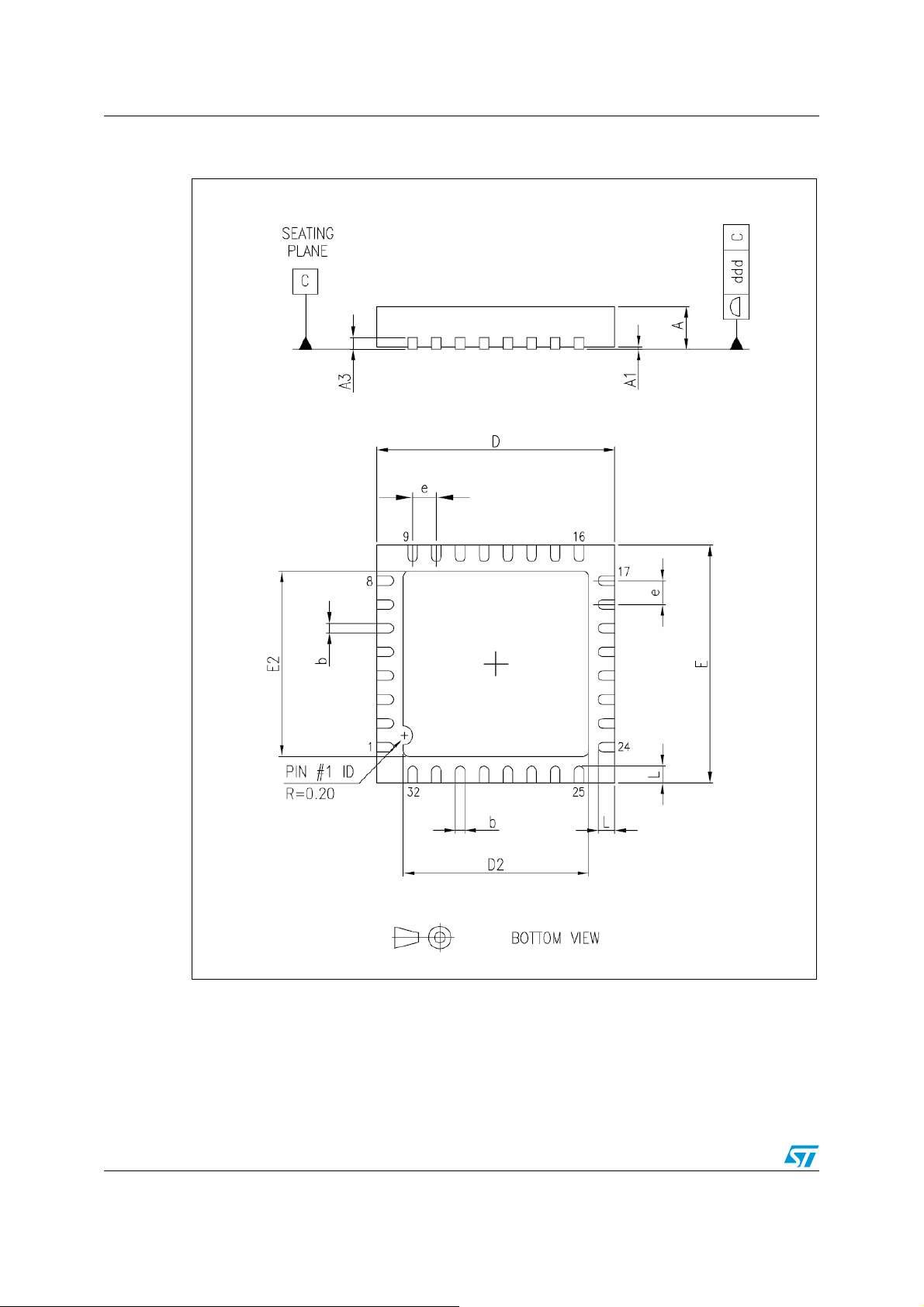
PM6680A Package mechanical data
10 Package mechanical data
In order to meet environmental requirements, ST offers these devices in ECOPACK®
packages. These packages have a Lead-free second level interconnect. The category of
second Level Interconnect is marked on the package and on the inner box label, in
compliance with JEDEC Standard JESD97. The maximum ratings related to soldering
conditions are also marked on the inner box label. ECOPACK is an ST trademark.
ECOPACK specifications are available at: www.st.com.
Table 16. VFQFPN 5x5 mechanical data (mm)
Dim Min Typ Max
A 0.80 0.90 1.00
A1 0 0.02 0.05
A3 0.20
b 0.18 0.25 0.30
D 4.85 5.00 5.15
D2 See exposed pad variations
E 4.85 5.00 5.15
E2 See exposed pad variations
e 0.50
L 0.30 0.40 0.50
ddd 0.05
1. Dimensions D2 & E2 are not in accordance with JEDEC.
Table 17. Exposed pad variations
(1)
(1)
D2 E2
Min Typ Max Min Typ Max
2.90 3.10 3.20 2.90 3.10 3.20
Note: 1 VFQFPN stands for Thermally Enhanced Very thin Fine pitch Quad Flat Package No lead.
Very thin: A=1.00 mm Max.
2 Dimensions D2 & E2 are not in accordance with JEDEC.
45/48
Page 46
Package mechanical data PM6680A
Figure 42. Package dimensions
46/48
Page 47

PM6680A Revision history
11 Revision history
Table 18. Document revision history
Date Revision Changes
12-Oct-2006 1 Initial release.
17-Dec-2007 2
Added Section 5: Typical operating characteristics on page 12 and
Section 9: Design guidelines on page 30
47/48
Page 48

PM6680A
Please Read Carefully:
Information in this document is provided solely in connection with ST products. STMicroelectronics NV and its subsidiaries (“ST”) reserve the
right to make changes, corrections, modifications or improvements, to this document, and the products and services described herein at any
time, without notice.
All ST products are sold pursuant to ST’s terms and conditions of sale.
Purchasers are solely responsible for the choice, selection and use of the ST products and services described herein, and ST assumes no
liability whatsoever relating to the choice, selection or use of the ST products and services described herein.
No license, express or implied, by estoppel or otherwise, to any intellectual property rights is granted under this document. If any part of this
document refers to any third party products or services it shall not be deemed a license grant by ST for the use of such third party products
or services, or any intellectual property contained therein or considered as a warranty covering the use in any manner whatsoever of such
third party products or services or any intellectual property contained therein.
UNLESS OTHERWISE SET FORTH IN ST’S TERMS AND CONDITIONS OF SALE ST DISCLAIMS ANY EXPRESS OR IMPLIED
WARRANTY WITH RESPECT TO THE USE AND/OR SALE OF ST PRODUCTS INCLUDING WITHOUT LIMITATION IMPLIED
WARRANTIES OF MERCHANTABILITY, FITNESS FOR A PARTICULAR PURPOSE (AND THEIR EQUIVALENTS UNDER THE LAWS
OF ANY JURISDICTION), OR INFRINGEMENT OF ANY PATENT, COPYRIGHT OR OTHER INTELLECTUAL PROPERTY RIGHT.
UNLESS EXPRESSLY APPROVED IN WRITING BY AN AUTHORIZED ST REPRESENTATIVE, ST PRODUCTS ARE NOT
RECOMMENDED, AUTHORIZED OR WARRANTED FOR USE IN MILITARY, AIR CRAFT, SPACE, LIFE SAVING, OR LIFE SUSTAINING
APPLICATIONS, NOR IN PRODUCTS OR SYSTEMS WHERE FAILURE OR MALFUNCTION MAY RESULT IN PERSONAL INJURY,
DEATH, OR SEVERE PROPERTY OR ENVIRONMENTAL DAMAGE. ST PRODUCTS WHICH ARE NOT SPECIFIED AS "AUTOMOTIVE
GRADE" MAY ONLY BE USED IN AUTOMOTIVE APPLICATIONS AT USER’S OWN RISK.
Resale of ST products with provisions different from the statements and/or technical features set forth in this document shall immediately void
any warranty granted by ST for the ST product or service described herein and shall not create or extend in any manner whatsoever, any
liability of ST.
ST and the ST logo are trademarks or registered trademarks of ST in various countries.
Information in this document supersedes and replaces all information previously supplied.
The ST logo is a registered trademark of STMicroelectronics. All other names are the property of their respective owners.
© 2007 STMicroelectronics - All rights reserved
STMicroelectronics group of companies
Australia - Belgium - Brazil - Canada - China - Czech Republic - Finland - France - Germany - Hong Kong - India - Israel - Italy - Japan -
Malaysia - Malta - Morocco - Singapore - Spain - Sweden - Switzerland - United Kingdom - United States of America
www.st.com
48/48
 Loading...