

No Rsense dual step-down controller with adjustable voltages
Features
■ 6 V to 28 V input voltage range
■ Adjustable output voltages
■ 5 V always voltage available deliver 100 mA
peak current
■ 1.237 V ± 1% reference voltage available
■ Lossless
MOSFETs R
■ Negative current limit
■ Soft-start internally fixed at 2ms
■ Soft output discharge
■ Latched OVP and UVP
■ Selectable pulse skipping at light loads
■ Selectable minimum frequency (33 kHz) in
pulse skip mode
■ 4 mW maximum quiescent power
■ Independent power good signals
■ Output voltage ripple compensation
Applications
■ Notebook computers
■ Tablet PC or slates
■ Mobile system power supply
■ 3-4 cells Li+ battery powered devices
current sensing using low side
DS(on)
PM6680
for notebook system power
VFQFPN-32 5X5
Description
PM6680 is a dual step-down controller
specifically designed to provide extremely high
efficiency conversion, with lossless current
sensing technique. The constant on-time
architecture assures fast load transient response
and the embedded voltage feed-forward provides
nearly constant switching frequency operation. An
embedded integrator control loop compensates
the DC voltage error due to the output ripple.
Pulse skipping technique increases efficiency at
very light load. Moreover a minimum switching
frequency of 33kHz is selectable to avoid audio
noise issues. The PM6680 provides a selectable
switching frequency, allowing three different
values of switching frequencies for the two
switching sections. The output voltages OUT1
and OUT2 can be adjusted from 0.9 V to 5.5 V
and from 0.9 V to 3.3 V respectively.
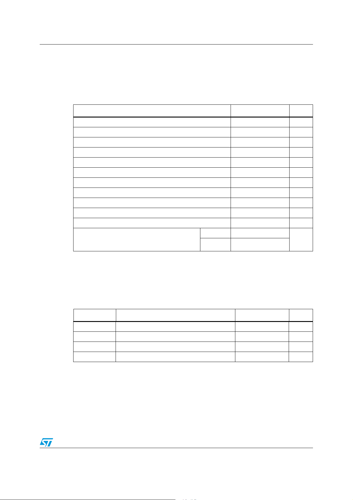
Table 1. Device summary
Order codes Package Packaging
PM6680
VFQFPN-32 5mm x 5mm (Exposed pad)
PM6680TR Tape and reel
January 2008 Rev 7 1/49
Tr ay
www.st.com
49

Contents PM6680
Contents
1 Simplified application schematic . . . . . . . . . . . . . . . . . . . . . . . . . . . . . . . 4
2 Electrical data . . . . . . . . . . . . . . . . . . . . . . . . . . . . . . . . . . . . . . . . . . . . . . 5
2.1 Maximum rating . . . . . . . . . . . . . . . . . . . . . . . . . . . . . . . . . . . . . . . . . . . . . 5
2.2 Thermal data . . . . . . . . . . . . . . . . . . . . . . . . . . . . . . . . . . . . . . . . . . . . . . . 5
3 Pin settings . . . . . . . . . . . . . . . . . . . . . . . . . . . . . . . . . . . . . . . . . . . . . . . . 6
3.1 Connections . . . . . . . . . . . . . . . . . . . . . . . . . . . . . . . . . . . . . . . . . . . . . . . . 6
3.2 Functions . . . . . . . . . . . . . . . . . . . . . . . . . . . . . . . . . . . . . . . . . . . . . . . . . . 7
4 Electrical characteristics . . . . . . . . . . . . . . . . . . . . . . . . . . . . . . . . . . . . 10
5 Typical operating characteristics . . . . . . . . . . . . . . . . . . . . . . . . . . . . . 13
6 Block diagram . . . . . . . . . . . . . . . . . . . . . . . . . . . . . . . . . . . . . . . . . . . . . 18
7 Device description . . . . . . . . . . . . . . . . . . . . . . . . . . . . . . . . . . . . . . . . . 19
7.1 Constant On time PWM control . . . . . . . . . . . . . . . . . . . . . . . . . . . . . . . . 19
7.2 Constant on time architecture . . . . . . . . . . . . . . . . . . . . . . . . . . . . . . . . . 21
7.3 Output ripple compensation and loop stability . . . . . . . . . . . . . . . . . . . . . 22
7.4 Pulse skip mode . . . . . . . . . . . . . . . . . . . . . . . . . . . . . . . . . . . . . . . . . . . . 23
7.5 No-audible skip mode . . . . . . . . . . . . . . . . . . . . . . . . . . . . . . . . . . . . . . . . 23
7.6 Current limit . . . . . . . . . . . . . . . . . . . . . . . . . . . . . . . . . . . . . . . . . . . . . . . 24
7.7 Soft start and soft end . . . . . . . . . . . . . . . . . . . . . . . . . . . . . . . . . . . . . . . 26
7.8 Gate drivers . . . . . . . . . . . . . . . . . . . . . . . . . . . . . . . . . . . . . . . . . . . . . . . 27
7.9 Reference voltage and bandgap . . . . . . . . . . . . . . . . . . . . . . . . . . . . . . . 27
7.10 Internal linear regulator . . . . . . . . . . . . . . . . . . . . . . . . . . . . . . . . . . . . . . 28
7.11 Power up sequencing and operative modes . . . . . . . . . . . . . . . . . . . . . . . 28
7.12 Monitoring and protections . . . . . . . . . . . . . . . . . . . . . . . . . . . . . . . . . . . . 29
7.12.1 Power good signals . . . . . . . . . . . . . . . . . . . . . . . . . . . . . . . . . . . . . . . . 29
7.12.2 Thermal protection . . . . . . . . . . . . . . . . . . . . . . . . . . . . . . . . . . . . . . . . . 29
7.12.3 Overvoltage protection . . . . . . . . . . . . . . . . . . . . . . . . . . . . . . . . . . . . . . 29
7.12.4 Undervoltage protection . . . . . . . . . . . . . . . . . . . . . . . . . . . . . . . . . . . . . 29
2/49

PM6680 Contents
7.13 Design guidelines . . . . . . . . . . . . . . . . . . . . . . . . . . . . . . . . . . . . . . . . . . . 30
7.13.1 Switching frequency . . . . . . . . . . . . . . . . . . . . . . . . . . . . . . . . . . . . . . . . 30
7.13.2 Inductor selection . . . . . . . . . . . . . . . . . . . . . . . . . . . . . . . . . . . . . . . . . . 30
7.13.3 Output capacitor . . . . . . . . . . . . . . . . . . . . . . . . . . . . . . . . . . . . . . . . . . 31
7.13.4 Input capacitors selection . . . . . . . . . . . . . . . . . . . . . . . . . . . . . . . . . . . 32
7.13.5 Power MOSFETs . . . . . . . . . . . . . . . . . . . . . . . . . . . . . . . . . . . . . . . . . . 33
7.13.6 Closing the integrator loop . . . . . . . . . . . . . . . . . . . . . . . . . . . . . . . . . . . 35
7.13.7 Other parts design . . . . . . . . . . . . . . . . . . . . . . . . . . . . . . . . . . . . . . . . . 38
7.13.8 Design example . . . . . . . . . . . . . . . . . . . . . . . . . . . . . . . . . . . . . . . . . . . 40
8 Package mechanical data . . . . . . . . . . . . . . . . . . . . . . . . . . . . . . . . . . . . 44
9 Revision history . . . . . . . . . . . . . . . . . . . . . . . . . . . . . . . . . . . . . . . . . . . 46
3/49

List of figures PM6680
List of figures
Figure 1. Simplified application schematic . . . . . . . . . . . . . . . . . . . . . . . . . . . . . . . . . . . . . . . . . . . . . . 6
Figure 2. Pin connection (Through top view) . . . . . . . . . . . . . . . . . . . . . . . . . . . . . . . . . . . . . . . . . . . . 8
Figure 3. 1.5V output efficiency vs load current . . . . . . . . . . . . . . . . . . . . . . . . . . . . . . . . . . . . . . . . . 15
Figure 4. 1.05V output efficiency vs load current . . . . . . . . . . . . . . . . . . . . . . . . . . . . . . . . . . . . . . . . 15
Figure 5. PWM no load input battery vs input voltage . . . . . . . . . . . . . . . . . . . . . . . . . . . . . . . . . . . . 15
Figure 6. Skip no load battery current . . . . . . . . . . . . . . . . . . . . . . . . . . . . . . . . . . . . . . . . . . . . . . . . 15
Figure 7. No-audible skip no load battery current vs input voltage . . . . . . . . . . . . . . . . . . . . . . . . . . 16
Figure 8. Stand-by mode input battery current vs input voltage . . . . . . . . . . . . . . . . . . . . . . . . . . . . 16
Figure 9. Shutdown mode input battery current vs input voltage . . . . . . . . . . . . . . . . . . . . . . . . . . . . 16
Figure 10. 1.5V switching frequency vs load current . . . . . . . . . . . . . . . . . . . . . . . . . . . . . . . . . . . . . . 16
Figure 11. 1.05V switching frequency vs load current . . . . . . . . . . . . . . . . . . . . . . . . . . . . . . . . . . . . . 16
Figure 12. LDO5 vs output current. . . . . . . . . . . . . . . . . . . . . . . . . . . . . . . . . . . . . . . . . . . . . . . . . . . . 16
Figure 13. 1.5V voltage regulation vs load current . . . . . . . . . . . . . . . . . . . . . . . . . . . . . . . . . . . . . . . 17
Figure 14. 1.05V voltage regulation vs load current . . . . . . . . . . . . . . . . . . . . . . . . . . . . . . . . . . . . . . 17
Figure 15. Voltage reference vs load current. . . . . . . . . . . . . . . . . . . . . . . . . . . . . . . . . . . . . . . . . . . . 17
Figure 16. OUT1, OUT2 and LDO5 power-up . . . . . . . . . . . . . . . . . . . . . . . . . . . . . . . . . . . . . . . . . . . 17
Figure 17. 1.5V load transient . . . . . . . . . . . . . . . . . . . . . . . . . . . . . . . . . . . . . . . . . . . . . . . . . . . . . . . 17
Figure 18. 1.05V load transient . . . . . . . . . . . . . . . . . . . . . . . . . . . . . . . . . . . . . . . . . . . . . . . . . . . . . . 17
Figure 19. 1.5V soft start (0.25Ω load). . . . . . . . . . . . . . . . . . . . . . . . . . . . . . . . . . . . . . . . . . . . . . . . . 18
Figure 20. 1.05V soft start (0.175Ω load). . . . . . . . . . . . . . . . . . . . . . . . . . . . . . . . . . . . . . . . . . . . . . . 18
Figure 21. 1.5V soft end (No load) . . . . . . . . . . . . . . . . . . . . . . . . . . . . . . . . . . . . . . . . . . . . . . . . . . . . 18
Figure 22. 1.05V soft end (No load) . . . . . . . . . . . . . . . . . . . . . . . . . . . . . . . . . . . . . . . . . . . . . . . . . . . 18
Figure 23. 1.5V soft end (1Ω Load) . . . . . . . . . . . . . . . . . . . . . . . . . . . . . . . . . . . . . . . . . . . . . . . . . . . 18
Figure 24. 1.05V soft end (1Ω Load) . . . . . . . . . . . . . . . . . . . . . . . . . . . . . . . . . . . . . . . . . . . . . . . . . . 18
Figure 25. 1.5V no-audible skip mode . . . . . . . . . . . . . . . . . . . . . . . . . . . . . . . . . . . . . . . . . . . . . . . . . 19
Figure 26. 1.05V no-audible skip mode . . . . . . . . . . . . . . . . . . . . . . . . . . . . . . . . . . . . . . . . . . . . . . . . 19
Figure 27. Functional block diagram . . . . . . . . . . . . . . . . . . . . . . . . . . . . . . . . . . . . . . . . . . . . . . . . . . 20
Figure 28. Constant ON time PWM control . . . . . . . . . . . . . . . . . . . . . . . . . . . . . . . . . . . . . . . . . . . . . 22
Figure 29. Constant on-time block diagram . . . . . . . . . . . . . . . . . . . . . . . . . . . . . . . . . . . . . . . . . . . . . 23
Figure 30. Circuitry for output ripple compensation . . . . . . . . . . . . . . . . . . . . . . . . . . . . . . . . . . . . . . . 24
Figure 31. PWM and pulse skip mode inductor current . . . . . . . . . . . . . . . . . . . . . . . . . . . . . . . . . . . . 25
Figure 32. No audible skip mode . . . . . . . . . . . . . . . . . . . . . . . . . . . . . . . . . . . . . . . . . . . . . . . . . . . . . 26
Figure 33. RDSON sensing technique . . . . . . . . . . . . . . . . . . . . . . . . . . . . . . . . . . . . . . . . . . . . . . . . . 26
Figure 34. Current waveforms in current limit conditions . . . . . . . . . . . . . . . . . . . . . . . . . . . . . . . . . . . 27
Figure 35. Soft start waveforms . . . . . . . . . . . . . . . . . . . . . . . . . . . . . . . . . . . . . . . . . . . . . . . . . . . . . . 28
Figure 36. Circuitry for output ripple compensation . . . . . . . . . . . . . . . . . . . . . . . . . . . . . . . . . . . . . . . 37
Figure 37. Virtual ESR network . . . . . . . . . . . . . . . . . . . . . . . . . . . . . . . . . . . . . . . . . . . . . . . . . . . . . . 38
Figure 38. VIN pin filter . . . . . . . . . . . . . . . . . . . . . . . . . . . . . . . . . . . . . . . . . . . . . . . . . . . . . . . . . . . . 40
Figure 39. Inductor current waveforms . . . . . . . . . . . . . . . . . . . . . . . . . . . . . . . . . . . . . . . . . . . . . . . . 41
Figure 40. Bootstrap circuit . . . . . . . . . . . . . . . . . . . . . . . . . . . . . . . . . . . . . . . . . . . . . . . . . . . . . . . . . 41
Figure 41. Current paths, ground connection and driver traces layout . . . . . . . . . . . . . . . . . . . . . . . . 44
Figure 42. Package dimensions. . . . . . . . . . . . . . . . . . . . . . . . . . . . . . . . . . . . . . . . . . . . . . . . . . . . . . 47
4/49

PM6680 List of tables
List of tables
Table 1. Device summary . . . . . . . . . . . . . . . . . . . . . . . . . . . . . . . . . . . . . . . . . . . . . . . . . . . . . . . . . . 1
Table 2. Absolute maximum ratings . . . . . . . . . . . . . . . . . . . . . . . . . . . . . . . . . . . . . . . . . . . . . . . . . . 7
Table 3. Thermal data. . . . . . . . . . . . . . . . . . . . . . . . . . . . . . . . . . . . . . . . . . . . . . . . . . . . . . . . . . . . . 7
Table 4. Pin functions . . . . . . . . . . . . . . . . . . . . . . . . . . . . . . . . . . . . . . . . . . . . . . . . . . . . . . . . . . . . . 9
Table 5. Electrical characteristics . . . . . . . . . . . . . . . . . . . . . . . . . . . . . . . . . . . . . . . . . . . . . . . . . . . 12
Table 6. FSEL pin selection: typical switching frequency . . . . . . . . . . . . . . . . . . . . . . . . . . . . . . . . 22
Table 7. V5SW multifunction pin. . . . . . . . . . . . . . . . . . . . . . . . . . . . . . . . . . . . . . . . . . . . . . . . . . . . 30
Table 8. Operatives modes. . . . . . . . . . . . . . . . . . . . . . . . . . . . . . . . . . . . . . . . . . . . . . . . . . . . . . . . 30
Table 9. Protections and operatives modes . . . . . . . . . . . . . . . . . . . . . . . . . . . . . . . . . . . . . . . . . . . 31
Table 10. Inductor manufacturer. . . . . . . . . . . . . . . . . . . . . . . . . . . . . . . . . . . . . . . . . . . . . . . . . . . . . 33
Table 11. Output capacitor manufacturer . . . . . . . . . . . . . . . . . . . . . . . . . . . . . . . . . . . . . . . . . . . . . . 34
Table 12. Input capacitor manufacturer . . . . . . . . . . . . . . . . . . . . . . . . . . . . . . . . . . . . . . . . . . . . . . . 34
Table 13. High side MOSFET manufacturer. . . . . . . . . . . . . . . . . . . . . . . . . . . . . . . . . . . . . . . . . . . . 35
Table 14. Low side MOSFET manufacturer . . . . . . . . . . . . . . . . . . . . . . . . . . . . . . . . . . . . . . . . . . . . 36
Table 15. Dual MOSFET manufacturer . . . . . . . . . . . . . . . . . . . . . . . . . . . . . . . . . . . . . . . . . . . . . . . 36
Table 16. Shottky diode manufacturer . . . . . . . . . . . . . . . . . . . . . . . . . . . . . . . . . . . . . . . . . . . . . . . . 36
Table 17. VFQFPN 5x5x1.0 32L Pitch 0.50 . . . . . . . . . . . . . . . . . . . . . . . . . . . . . . . . . . . . . . . . . . . . 46
Table 18. Exposed pad variations . . . . . . . . . . . . . . . . . . . . . . . . . . . . . . . . . . . . . . . . . . . . . . . . . . . 46
Table 19. Document revision history . . . . . . . . . . . . . . . . . . . . . . . . . . . . . . . . . . . . . . . . . . . . . . . . . 48
5/49
Simplified application schematic PM6680
O
O
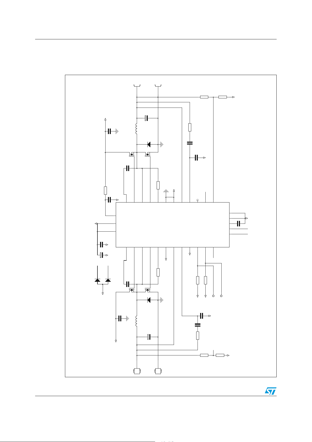
1 Simplified application schematic
Figure 1. Simplified application schematic
1
VIN
PGND
9
10
SGND
VIN
19
LDO5
V+
18
VCC
31
11
BOOT2
HGATE2
1
SGND
+
PGND
SGND
SGND
PGND
12
14
1
8
13
LGATE2
PHASE2
PGND
CSENSE2
2
OUT2
SGND
PM6680
FB1
6
28
7
NC
FB1
FB2
COMP2
FSEL
3
SKIP
VREF
EN1
EN2
SGND
24
32
4
BOOT1
SGND
+
SGND
BOOT1
BOOT2
V+
HGATE1
23
22
PGND
LGATE1
PHASE1
21
+
VIN
1
OUT1+
6/49
SGND 2
PGOOD 1
PGOOD 2
CSENSE1
V5SW
OUT1
COMP1
20
17
29
3025161526
SGND
SGND
PGND
1
OUT1-
V+
SHD N
5
27
PGOOD1
V+
PGOOD2
SGND
FB1
SGND
PM6680 Electrical data
2 Electrical data
2.1 Maximum rating
Table 2. Absolute maximum ratings
Parameter Value Unit
V5SW, LDO5 to PGND -0.3 to 6 V
VIN to PGND -0.3 to 36 V
HGATEx and BOOTx, to PHASEx -0.3 to 6 V
PHASEx to PGND -0.6
CSENSEx , to PGND -0.6 to 42 V
CSENSEx to BOOTx -6 to 0.3 V
LGATEx to PGND -0.3
FBx, COMPx, SKIP, , FSEL,VREF to SGND1,SGND2 -0.3 to Vcc +0.3 V
PGND to SGND1,SGND2 -0.3 to 0.3 V
SHDN,PGOODx, OUTx, VCC, ENx to SGND1,SGND2 -0.3 to 6 V
(1)
to36
(2)
to LDO5 +0.3
V
V
Power dissipation at TA = 25ºC 2.8 W
Maximum withstanding voltage range test condition:
CDF-AEC-Q100-002- “Human Body Model”
acceptance criteria: “Normal Performance”
1. PHASE to PGND up to -2.5 V for t<10 ns
2. LGATEx to PGND up to -1 V for t<40 ns
2.2 Thermal data
Table 3. Thermal data
Symbol Parameter Value Unit
R
thJA
T
STG
T
J
T
A
Thermal resistance junction to ambient 35 °C/W
Storage temperature range -50 to 150 °C
Junction operating temperature range -40 to 125 °C
Operating ambient temperature range -40 to 85 °C
VIN ±1000
V
Other pins ±2000
7/49
Pin settings PM6680
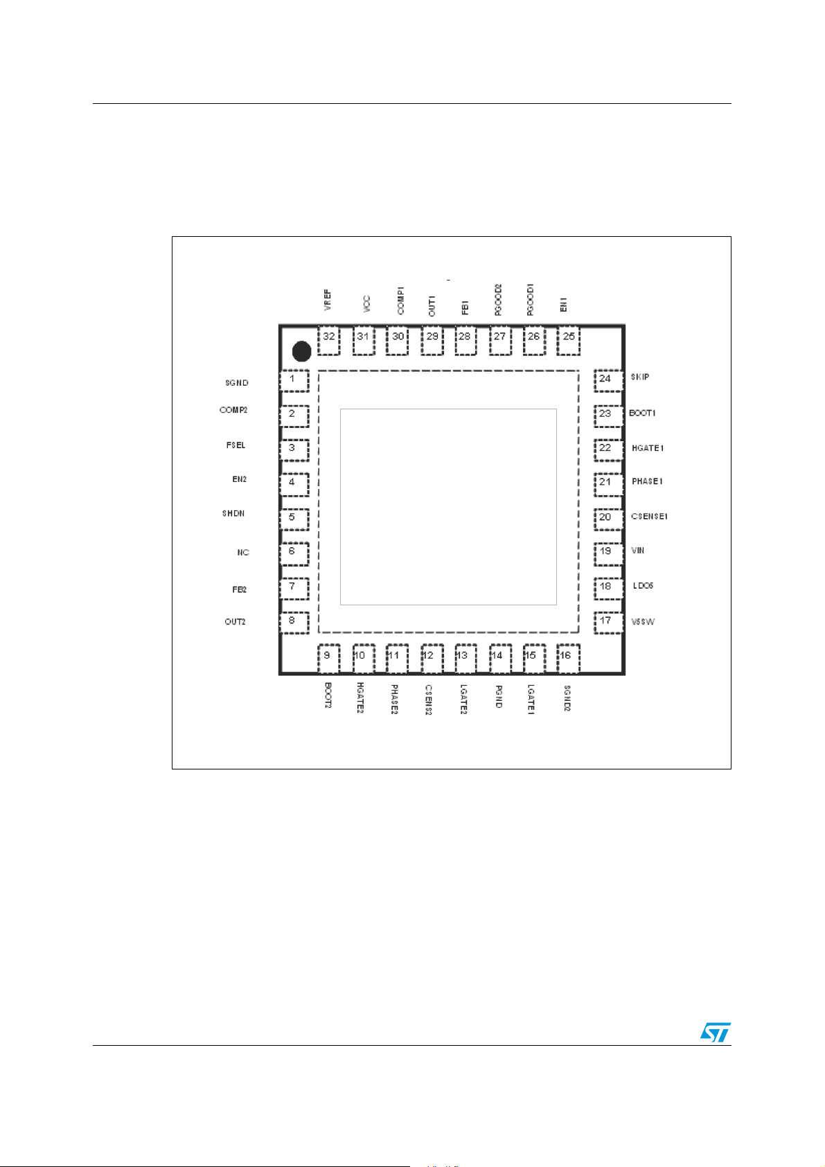
3 Pin settings
3.1 Connections
Figure 2. Pin connection (Through top view)
PM6680
8/49

PM6680 Pin settings
3.2 Functions
Table 4. Pin functions
N° Pin Function
Signal ground. Reference for internal logic circuitry. It must be connected to
1SGND1
2 COMP2 DC voltage error compensation pin for the switching section 2
3 FSEL
4EN2
5 SHDN
6 NC Not connected.
7FB2
8OUT2
9BOOT2
the signal ground plan of the power supply. The signal ground plan and the
power ground plan must be connected together in one point near the PGND
pin.
Frequency selection pin. It provides a selectable switching frequency,
allowing three different values of switching frequencies for the switching
sections.
Enable input for the switching section 2.
• The section 2 is enabled applying a voltage greater than 2.4 V to this pin.
• The section 2 is disabled applying a voltage lower than 0.8 V.
When the section is disabled the High Side gate driver goes low and Low
Side gate driver goes high. If both EN1 and EN2 pins are low and SHDN pin
is high the device enters in standby mode.
Shutdown control input.
• The device switch off if the SHDN voltage is lower than the device off
threshold (Shutdown mode)
• The device switch on if the SHDN voltage is greater than the device on
threshold.
The SHDN pin can be connected to the battery through a voltage divider to
program an undervoltage lockout. In shutdown mode, the gate drivers of the
two switching sections are in high impedance (high-Z).
Feedback input for the switching section 2 This pin is connected to a
resistive voltage-divider from OUT2 to PGND to adjust the output voltage
from 0.9 V to 3.3 V.
Output voltage sense for the switching section 2.This pin must be directly
connected to the output voltage of the switching section.
Bootstrap capacitor connection for the switching section 2. It supplies the
high-side gate driver.
10 HGATE2
11 PHASE2
12 CSENSE2
13 LGATE2 Low-side gate driver output for the section 2.
14 PGND
15 LGATE1 Low-side gate driver output for the section 1.
High-side gate driver output for section 2. This is the floating gate driver
output.
Switch node connection and return path for the high side driver for the
section 2.It is also used as negative current sense input.
Positive current sense input for the switching section 2. This pin must be
connected through a resistor to the drain of the synchronous rectifier
(R
supply controller.
Power ground. This pin must be connected to the power ground plan of the
power supply.
sensing) to obtain a positive current limit threshold for the power
DSON
9/49

Pin settings PM6680
Table 4. Pin functions (continued)
N° Pin Function
16 SGND2
17 V5SW
18 LDO5
19 VIN
20 CSENSE1
21 PHASE1
22 HGATE1
23 BOOT1
24 SKIP
25 EN1
26 PGOOD1
27 PGOOD2
28 FB1
Signal ground for analog circuitry. It must be connected to the signal ground
plan of the power supply.
Internal 5 V regulator bypass connection.
• If V5SW is connected to OUT5 (or to an external 5 V supply) and V5SW is
greater than 4.9 V, the LDO5 regulator shuts down and the LDO5 pin is
directly connected to OUT5 through a 3 Ω (max) switch.
If V5SW is connected to GND, the LDO5 linear regulator is always on.
5 V internal regulator output. It can provide up to 100mA peak current.
LDO5 pin supplies embedded low side gate drivers and an external load.
Device supply voltage input and battery voltage sense. A bypass filter (4 Ω
and 4.7 µF) between the battery and this pin is recommended.
Positive current sense input for the switching section 1. This pin must be
connected through a resistor to the drain of the synchronous rectifier
(R
supply controller.
Switch node connection and return path for the high side driver for the
section 1.It is also used as negative current sense input.
High-side gate driver output for section 1. This is the floating gate driver
output.
Bootstrap capacitor connection for the switching section 1. It supplies the
high-side gate driver.
Pulse skipping mode control input.
• If the pin is connected to LDO5 the PWM mode is enabled.
• If the pin is connected to GND, the pulse skip mode is enabled.
• If the pin is connected to VREF the pulse skip mode is enabled but the
switching frequency is kept higher than 33 kHz (No-audible pulse skip
mode).
Enable input for the switching section 1.
• The section 1 is enabled applying a voltage greater than 2.4 V to this pin.
• The section 1 is disabled applying a voltage lower than 0.8 V.
When the section is disabled the High Side gate driver goes low and Low
Side gate driver goes high.
Power Good output signal for the section 1. This pin is an open drain output
and when the output of the switching section 1 is out of +/- 10 % of its
nominal value.It is pulled down.
Power Good output signal for the section 2. This pin is an open drain output
and when the output of the switching section 2 is out of +/- 10 % of its
nominal value.It is pulled down.
Feedback input for the switching section 1. This pin is connected to a
resistive voltage-divider from OUT1 to PGND to adjust the output voltage
from 0.9 V to 5.5 V.
sensing) to obtain a positive current limit threshold for the power
DSON
10/49

PM6680 Pin settings
Table 4. Pin functions (continued)
N° Pin Function
29 OUT1
30 COMP1 DC voltage error compensation pin for the switching section 1.
31 VCC
32 VREF
Output voltage sense for the switching section 1.This pin must be directly
connected to the output voltage of the switching section.
Device Supply Voltage pin. It supplies all the internal analog circuitry except
the gate drivers (see LDO5). Connect this pin to LDO5.
Internal 1.237 V high accuracy voltage reference. It can deliver 50 uA.
Bypass to SGND with a 100 nF capacitor to reduce noise.
11/49
Electrical characteristics PM6680
4 Electrical characteristics
Table 5. Electrical characteristics
V
= 12 V, TA = 0 °C to 85 °C, unless otherwise specified
IN
(1)
Symbol Parameter Test condition Min Typ Max Unit
Supply section
VIN
Input voltage range
Vout = Vref, LDO5 in
regulation
5.5 28 V
Vcc IC supply voltage 4.5 5.5 V
Turn-on voltage threshold 4.8 4.9 V
V
V5SW
Turn-off voltage threshold 4.6 4.75 V
Hysteresis 20 50 mV
V
V5SW
Rdson
Maximum operating range 5.5 V
LDO5 internal bootstrap
switch resistance
OUTx,OUTx discharge-mode
on-resistance
V5SW > 4.9 1.8 3 Ω
18 25 Ω
OUTx,OUTx discharge-mode
synchronous rectifier
0.2 0.36 0.6 V
Turn-on level
Pin Operating power consumption
Ish Operating current sunk by V
Isb Operating current sunk by V
FBx > VREF, Vref in
regulation, V5WS to 5 V
SHDN connected to GND, 14 18 µA
IN
ENx to GND, V5SW to GND 190 250 µA
IN
4mW
Shutdown section
V
SHDN
Device off threshold 0.8 0.85 0.9 V
Soft start section
Soft start ramp time 2 3.5 ms
Current limit and zero crossing comparator
Device on threshold 1.2 1.5 1.7 V
I
CSENSE
Input bias current limit 90 100 110 µA
Comparator offset VCSENSE-VPGND -6 6 mV
Zero crossing comparator offset V
Fixed negative current limit
threshold
PGND
V
PGND
- V
- V
12/49
PHASE
PHASE
-1 11 mV
-120 mV
PM6680 Electrical characteristics
Table 5. Electrical characteristics (continued)
V
= 12 V, TA = 0 °C to 85 °C, unless otherwise specified
IN
(1)
Symbol Parameter Test condition Min Typ Max Unit
On time pulse width
OUT1=1.5 V 550 650 750
OUT2=1.05 V 230 270 315
OUT1=1.5 V 375 445 515
OUT2=1.05 V 175 210 245
OUT1=1.5 V 285 340 395
OUT2=1.05 V 125 150 175
Ton On time duration
FSEL to
GND
FSEL to
VREF
FSEL to
LDO5
OFF time
T
OFFMIN
Minimum off time 350 500 ns
Volt a g e re f e ren c e
V
REF
Voltage accuracy 4 V < V
Load regulation -100 µA< I
Undervoltage lockout fault
threshold
Falling edge of REF 0.95 mV
< 5.5 V 1.224 1.236 1.249 V
LDO5
< 100 µA -4 4 mV
REF
ns
Integrator
FB Voltage accuracy -909 900 909 mV
FB Input bias current 0.1 µA
Normal mode 250
Over voltage clamp
COMP
Under voltage clamp -150
Line regulation
Both SMPS, 6 V<Vin<28 V
(2)
0.004 %/V
LDO5 linear regulator
6 V<VIN<28 V ,
LDO5
< 50 mA
0 < I
4.9 5.0 5.1 V
6 V< VIN < 28 V,
= 20 mA
I
LDO5
> UVLO 270 330 400 mA
LDO5
,
0.004 %/V
V
I
LDO5
LDO5
LDO5 linear output voltage
LDO5 line regulation
LDO5 Current limit V
U L V O U n d e r V o l t a g e L o c k o u t o f L D O 5 3 . 9 4 4 4 . 1 3 V
mVPulse skip mode 60
13/49
Electrical characteristics PM6680
Table 5. Electrical characteristics (continued)
V
= 12 V, TA = 0 °C to 85 °C, unless otherwise specified
IN
(1)
Symbol Parameter Test condition Min Typ Max Unit
High and low gate drivers
HGATEx high state (pullup) 2.0 3 Ω
HGATE driver on-resistance
HGATEx low state
(pulldown)
1.6 2.7 Ω
LGATEx high state (pullup) 1.4 2.1 Ω
LGATE driver on-resistance
LGATEx low state (pulldown) 0.8 1.2 Ω
PGOOD pins UVP/OVP protections
OVP Over voltage threshold
UVP Under voltage threshold 65 68 71 %
Both SMPS sections with
respect to VREF.
Upper threshold
(VFB-VREF)
112 116 120 %
107 110 113 %
PGOOD1,2
I
PGOOD1,2
V
PGOOD1,2
Lower threshold
(VFB-VREF)
PGOOD leakage current V
PGOOD1,2
forced to 5.5 V 1 uA
Output low voltage ISink = 4 mA 150 250 mV
88 91 94 %
Thermal shutdown
T
SDN
Shutdown temperature 150 °C
Power management pins
SMPS disabled level 0.8
EN1,2
SMPS enabled level 2.4
Low level
FSEL Frequency selection range
High level
Pulse skip mode
SKIP
PWM mode
Input leakage current
1. TA = TJ, All parameters at operating temperature extremes are guaranteed by design and statistical analysis
(not production tested).
2. by design
3. by demoboard test
(3)
(3)
(3)
V
EN1,2
V
SKIP
V
SHDN
V
FSEL
(3)
(3)
(3)
1.0 V
V
-0.8
LDO5
1.0 V
V
-0.8
LDO5
= 0 to 5 V 1
= 0 to 5 V 1
= 0 to 5 V 1
= 0 to 5 V 1
0.5
LDO5
0.5
LDO5
-1.5
-1.5
V
VMiddle level
VUltrasonic mode
µA
14/49
PM6680 Typical operating characteristics
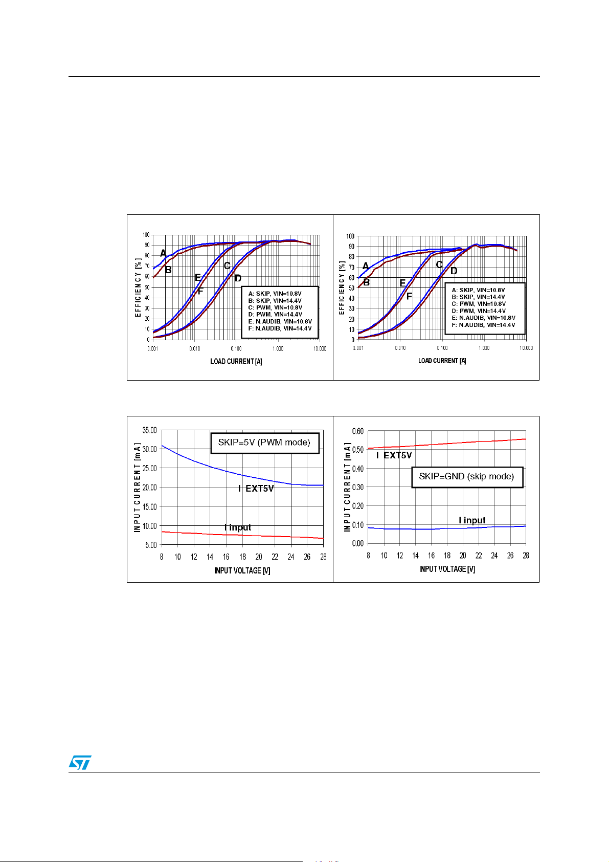
5 Typical operating characteristics
FSEL = GND (200/300 kHz), SKIP = GND (skip mode), V5SW = V5SW = EXT5V
(external 5 V power supply connected), input voltage VIN = 12 V, SHDN, EN1 and EN2 high,
OUT1 = 1.5 V, OUT2 = 1.05 V, no load unless specified)
Figure 3. 1.5 V output efficiency vs
load current
Figure 5. PWM no load input battery vs
input voltage
Figure 4. 1.05 V output efficiency vs
load current
Figure 6. Skip no load battery current
15/49
 Loading...