

Page 1
Complete DDR2/3 memory power supply controller
Features
■ Switching section (VDDQ)
– 4.5 V to 28 V input voltage range
– 0.9 V, ±1 % voltage reference
– 1.8 V (DDR2) or 1.5 V (DDR3) fixed output
voltages
– 0.9 V to 2.6 V adjustable output voltage
– 1.237 V ±1 % reference voltage available
– Very fast load transient response using
constant on-time control loop
–No R
MOSFET’s R
– Negative current limit
– Latched OVP and UVP
– Soft-start internally fixed at 3 ms
– Selectable pulse skipping at light load
– Selectable no-audible (33 kHz) pulse skip
mode
– Ceramic output capacitors supported
– Output voltage ripple compensation
■ VTT LDO and VTTREF
– 2 Apk LDO with foldback for VTT
– Remote VTT sensing
– High-Z VTT output in S3
– Ceramic output capacitors supported
– ±15 mA low noise buffered reference
Applications
■ DDR2/3 memory supply
■ Notebook computers
■ Handheld and PDAs
■ CPU and chipset I/O supplies
■ SSTL18, SSTL15 and HSTL bus termination
current sensing using low side
SENSE
DS(ON)
PM6670S
VFQFPN-24 4x4
Description
The device PM6670S is a complete DDR2/3
power supply regulator designed to meet JEDEC
specifications.
It integrates a constant on-time (COT) buck
controller, a 2 Apk sink/source low drop out
regulator and a 15 mA low noise buffered
reference.
The COT architecture assures fast transient
response supporting both electrolytic and ceramic
output capacitors. An embedded integrator
control loop compensates the DC voltage error
due to the output ripple.
The 2 Apk sink/source linear regulator provides
the memory termination voltage with fast load
transient response.
The device is fully compliant with system sleep
states S3 and S4/S5, providing LDO output high
impedance in suspend-to-RAM and tracking
discharge of all outputs in suspend-to-disk.
Table 1. Device summary
Order code Package Packaging
PM6670S
PM6670STR Tape and reel
VFQFPN-24 4x4
(Exposed pad)
Tube
February 2010 Doc ID 14432 Rev 4 1/54
www.st.com
54
Page 2

Contents PM6670S
Contents
1 Typical application circuit . . . . . . . . . . . . . . . . . . . . . . . . . . . . . . . . . . . . 4
2 Pin settings . . . . . . . . . . . . . . . . . . . . . . . . . . . . . . . . . . . . . . . . . . . . . . . . 5
2.1 Connections . . . . . . . . . . . . . . . . . . . . . . . . . . . . . . . . . . . . . . . . . . . . . . . . 5
2.2 Pin description . . . . . . . . . . . . . . . . . . . . . . . . . . . . . . . . . . . . . . . . . . . . . . 6
3 Electrical data . . . . . . . . . . . . . . . . . . . . . . . . . . . . . . . . . . . . . . . . . . . . . . 8
3.1 Maximum rating . . . . . . . . . . . . . . . . . . . . . . . . . . . . . . . . . . . . . . . . . . . . . 8
3.2 Thermal data . . . . . . . . . . . . . . . . . . . . . . . . . . . . . . . . . . . . . . . . . . . . . . . 8
3.3 Recommended operating conditions . . . . . . . . . . . . . . . . . . . . . . . . . . . . . 9
4 Electrical characteristics . . . . . . . . . . . . . . . . . . . . . . . . . . . . . . . . . . . . 10
5 Typical operating characteristics . . . . . . . . . . . . . . . . . . . . . . . . . . . . . 14
6 Block diagram . . . . . . . . . . . . . . . . . . . . . . . . . . . . . . . . . . . . . . . . . . . . . 19
7 Device description . . . . . . . . . . . . . . . . . . . . . . . . . . . . . . . . . . . . . . . . . 20
7.1 VDDQ section - constant on-time PWM controller . . . . . . . . . . . . . . . . . . 21
7.1.1 Constant-on-time architecture . . . . . . . . . . . . . . . . . . . . . . . . . . . . . . . . 23
7.1.2 Output ripple compensation and loop stability . . . . . . . . . . . . . . . . . . . . 24
7.1.3 Pulse-skip and no-audible pulse-skip modes . . . . . . . . . . . . . . . . . . . . . 28
7.1.4 Mode-of-operation selection . . . . . . . . . . . . . . . . . . . . . . . . . . . . . . . . . 30
7.1.5 Current sensing and current limit . . . . . . . . . . . . . . . . . . . . . . . . . . . . . . 31
7.1.6 POR, UVLO and soft-start . . . . . . . . . . . . . . . . . . . . . . . . . . . . . . . . . . . 32
7.1.7 Power Good signal . . . . . . . . . . . . . . . . . . . . . . . . . . . . . . . . . . . . . . . . . 33
7.1.8 VDDQ output discharge . . . . . . . . . . . . . . . . . . . . . . . . . . . . . . . . . . . . . 34
7.1.9 Gate drivers . . . . . . . . . . . . . . . . . . . . . . . . . . . . . . . . . . . . . . . . . . . . . . 35
7.1.10 Reference voltage and bandgap . . . . . . . . . . . . . . . . . . . . . . . . . . . . . . 35
7.1.11 Over voltage and under voltage protections . . . . . . . . . . . . . . . . . . . . . 36
7.1.12 Device thermal protection . . . . . . . . . . . . . . . . . . . . . . . . . . . . . . . . . . . 36
7.2 VTTREF buffered reference and VTT LDO section . . . . . . . . . . . . . . . . . 37
7.2.1 VTT and VTTREF Soft-Start . . . . . . . . . . . . . . . . . . . . . . . . . . . . . . . . . 37
7.2.2 VTTREF and VTT outputs discharge . . . . . . . . . . . . . . . . . . . . . . . . . . . 37
2/54 Doc ID 14432 Rev 4
Page 3

PM6670S Contents
7.3 S3 and S5 power management pins . . . . . . . . . . . . . . . . . . . . . . . . . . . . 38
8 Application information . . . . . . . . . . . . . . . . . . . . . . . . . . . . . . . . . . . . . 39
8.1 External components selection . . . . . . . . . . . . . . . . . . . . . . . . . . . . . . . . 39
8.1.1 Inductor selection . . . . . . . . . . . . . . . . . . . . . . . . . . . . . . . . . . . . . . . . . . 41
8.1.2 Input capacitor selection . . . . . . . . . . . . . . . . . . . . . . . . . . . . . . . . . . . . 42
8.1.3 Output capacitor selection . . . . . . . . . . . . . . . . . . . . . . . . . . . . . . . . . . . 43
8.1.4 MOSFETs selection . . . . . . . . . . . . . . . . . . . . . . . . . . . . . . . . . . . . . . . . 44
8.1.5 Diode selection . . . . . . . . . . . . . . . . . . . . . . . . . . . . . . . . . . . . . . . . . . . 46
8.1.6 VDDQ current limit setting . . . . . . . . . . . . . . . . . . . . . . . . . . . . . . . . . . . 47
8.1.7 All ceramic capacitors application . . . . . . . . . . . . . . . . . . . . . . . . . . . . . 48
9 Package mechanical data . . . . . . . . . . . . . . . . . . . . . . . . . . . . . . . . . . . . 51
10 Revision history . . . . . . . . . . . . . . . . . . . . . . . . . . . . . . . . . . . . . . . . . . . 53
Doc ID 14432 Rev 4 3/54
Page 4

Typical application circuit PM6670S
V
V
V
V
V
(
)
1 Typical application circuit
Figure 1. Application circuit
DDQ
LDO input
C
TTREF
C
OUT3
11
IN4
23
4
2
24
TT
1
C
OUT2
C
IN3
3 12 6 18 8
SEL
DSCG
AVCC
MODE
LDOIN
VTTREF
VTTSNS
VTT
VTTGND
PM6670S
SGND
PG
S3
5 15 14 13 7 10
R
LP
+5V
IN
C
IN2
VCC
VOSC
BOOT
HGATE
PHASE
LGATE
COMP
VREF
S5
C
BYP
CSNS
PGND
VSNS
C
BOOT
21
20
17
19
R
16
9
LIM
R
1
C
R
2
IN
L
DDQ
C
OUT
C
INT
4/54 Doc ID 14432 Rev 4
Page 5
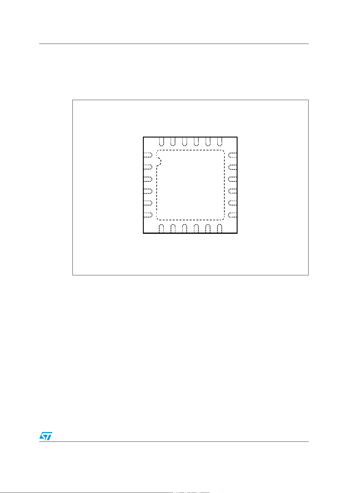
PM6670S Pin settings
2 Pin settings
2.1 Connections
Figure 2. Pin connection (through top view)
VTT
VTT
LDOIN
VTTGND
VTTGND
VTTSNS
VTTSNS
DDRSEL
DDRSEL
VTTREF
VTTREF
LDOIN
24
24
1
1
PM6670
PM6670
HGATE
HGATE
BOOT
BOOT
PHASE
PHASE
CSNS
CSNS
19
19
18
18
VCC
VCC
LGATE
LGATE
PGND
PGND
S
PG
PG
SGND
SGND
AVCC
AVCC
S3
S3
S5
6
6
7
7
VREF
VREF
VOSC
VOSC
VSNS
VSNS
MODE
MODE
COMP
COMP
13
13
12
12
DSCG
DSCG
S5
Doc ID 14432 Rev 4 5/54
Page 6

Pin settings PM6670S
2.2 Pin description
Table 2. Pin functions
N° Pin Function
1 VTTGND LDO power ground. Connect to negative terminal of VTT output capacitor.
2VTTSNS
3DDRSEL
4VTTREF
5SGND
6AVCC
7VREF
8VOSC
9 VSNS
10 MODE
LDO remote sensing. Connect as close as possible to the load via a low
noise PCB trace.
DDR voltage selector (if MODE is tied to VCC) or pulse-skip/no-audible
pulse-skip selector in adjustable mode (MODE voltage lower than 3 V). See
Section 7.1.4: Mode-of-operation selection on page 30.
Low noise buffered DDR reference voltage. A 22 nF (minimum) ceramic
bypass capacitor is required in order to achieve stability.
Ground reference for analog circuitry, control logic and VTTREF buffer.
Connect together with the thermal pad and VTTGND to a low impedance
ground plane. See the Application Note for details.
+5 V supply for internal logic. Connect to +5 V rail through a simple RC
filtering network.
High accuracy output voltage reference (1.237 V) for multilevel pins setting.
It can deliver up to 50 μA. Connect a 100 nF capacitor between VREF and
SGND in order to enhance noise rejection.
Frequency selection. Connect to the central tap of a resistor divider to set
the desired switching frequency. The pin cannot be left floating. See
Section 7: Device description on page 20
VDDQ output remote sensing. Discharge path for VDDQ in Non-Tracking
Discharge. Input for internal resistor divider that provides VDDQ/2 to
VTTREF and VTT. Connect as close as possible to the load via a low noise
PCB trace.
Mode of operation selector. If MODE pin voltage is higher than 4 V, the fixed
output mode is selected. If MODE pin voltage is lower than 4 V, it is used as
negative input of the error amplifier. See Section 7.1.4: Mode-of-operation
selection on page 30.
11 COMP
12 DSCG
13 S5
14 S3
15 PG
16 PGND Power ground for the switching section.
17 LGATE Low-side gate driver output.
6/54 Doc ID 14432 Rev 4
DC voltage error compensation Input for the switching section. Refer
Section 7.1.4: Mode-of-operation selection on page 30.
Discharge mode selection. Refer to Section 7.1.8: VDDQ output discharge
on page 34 for tracking/non-tracking discharge or no-discharge options.
Switching controller enable. Connect to S5 system status signal to meet S0S5 power management states compliance. See Section 7.3: S3 and S5
power management pins on page 38, S5 pin can't be left floating.
Linear regulator enable. Connect to S3 system status signal to meet S0-S5
power management states compliance. See Section 7.3: S3 and S5 power
management pins on page 38, S3 pin can't be left floating.
Power Good signal (open drain output). High when VDDQ output voltage is
within ±10 % of nominal value.
Page 7

PM6670S Pin settings
Table 2. Pin functions (continued)
N° Pin Function
18 VCC +5 V low-side gate driver supply. Bypass with a 100 nF capacitor to PGND.
Current sense input for the switching section. This pin must be connected
19 CSNS
20 PHASE Switch node connection and return path for the high-side gate driver.
21 HGATE High-side gate driver output
22 BOOT
23 LDOIN
24 VTT
through a resistor to the drain of the synchronous rectifier (R
set the current limit threshold.
Bootstrap capacitor connection. Positive supply input of the high-side gate
driver.
Linear regulator input. Connect to VDDQ in normal configuration or to a
lower supply to reduce the power dissipation. A 10 μF bypass ceramic
capacitor is suggested for noise rejection enhancement. See Section 7:
Device description on page 20
LDO linear regulator output. Bypass with a 20 μF (2x10 μF MLCC) filter
capacitor.
DSon
sensing) to
Doc ID 14432 Rev 4 7/54
Page 8

Electrical data PM6670S
3 Electrical data
3.1 Maximum rating
Table 3. Absolute maximum ratings
(1)
Symbol Parameter Value Unit
V
AVC C
V
VCC
AVCC to SGND -0.3 to 6
VCC to SGND -0.3 to 6
PGND, VTTGND to SGND -0.3 to 0.3
HGATE and BOOT to PHASE -0.3 to 6
HGATE and BOOT to PGND -0.3 to 44
V
PHASE
PHASE to SGND
LGATE to PGND -0.3 to V
CSNS, PG, S3, S5, DSCG, COMP, VSNS,
VOSC, VREF, MODE, DDRSEL to GND
VTTREF, VREF, VTT, VTTSNS to SGND -0.3 to V
LDOIN, VTT, VTTREF, LDOIN to VTTGND -0.3 to V
P
TOT
1. Free air operating conditions unless otherwise specified. Stresses beyond those listed under “absolute
maximum ratings” may cause permanent damage to the device. Exposure to absolute maximum rated
conditions for extended periods may affect device reliability.
2. PHASE to SGND up to -2.5 V for t < 10 ns
Power dissipation @TA = 25 °C 2.3 W
(2)
-0.3 to 38
-0.3 to V
CC
AVC C
AVC C
AVC C
+0.3
+ 0.3
+ 0.3
+ 0.3
V
3.2 Thermal data
Table 4. Thermal data
Symbol Parameter Value Unit
R
thJA
T
STG
T
A
T
J
8/54 Doc ID 14432 Rev 4
Thermal resistance junction to ambient 42 °C/W
Storage temperature range - 50 to 150 °C
Operating ambient temperature range - 40 to 85 °C
Junction operating temperature range - 40 to 125 °C
Page 9

PM6670S Electrical data
3.3 Recommended operating conditions
Table 5. Recommended operating conditions
Val ues
Symbol Parameter
Min Typ Max
Unit
V
AVC C
V
VCC
IN
Input voltage range 4.5 - 28
IC supply voltage 4.5 - 5.5
IC supply voltage 4.5 - 5.5
VV
Doc ID 14432 Rev 4 9/54
Page 10

Electrical characteristics PM6670S
4 Electrical characteristics
TA = 0 °C to 85 °C, VCC = AVCC = +5 V and LDOIN connected to VDDQ output if not
otherwise specified
Table 6. Electrical characteristics
Symbol Parameter Test condition
Supply section
I
IN
I
STR
I
SH
UVLO
Operating current
Operating current in STR
Operating current in
shutdown
AVCC under voltage lockout
upper threshold
AVCC under voltage lockout
lower threshold
UVLO hysteresis 70 mV
(a)
S3, S5, MODE and DDRSEL
connected to AVCC, no load on VTT
and VTTREF outputs.
VCC connected to AVCC
S5, MODE and DDRSEL connected
to AVCC, S3 tied to SGND, no load
on VTTREF.
VCC connected to AVCC
S3 and S5 tied to SGND.
Discharge mode active.
VCC connected to AVCC
Val ues
Unit
Min Typ Max
0.8 2
mA
0.6 1
110μA
4.1 4.25 4.4
V
3.85 4.0 4.1
ON-time (SMPS)
t
ON
On-time duration
MODE and
DDRSEL
high,
V
= 2 V
VSNS
VOSC
VOSC = 500 mV 390 450 510
OFF-time (SMPS)
t
OFFMIN
Minimum Off time 300 350 ns
Volt a g e re f e ren c e
Voltage accuracy 4.5 V < V
Load regulation -50 μA< I
< 25 V 1.224 1.237 1.249 V
IN
< 50 μA-44mV
VREF
Undervoltage lockout fault
threshold
a. TA = TJ. All parameters at operating temperature extremes are guaranteed by design and statistical analysis
(not production tested)
10/54 Doc ID 14432 Rev 4
= 300 mV 650 750 850
800
ns
Page 11
PM6670S Electrical characteristics
Table 6. Electrical characteristics (continued)
Val ues
Symbol Parameter Test condition
Min Typ Max
VDDQ output
Unit
MODE connected to AVCC,
DDRSEL tied to SGND, No load
MODE and DDRSEL connected to
AVCC, no load
V
VDDQ
VDDQ output voltage, DDR3
VDDQ output voltage, DDR2
Feedback accuracy -1.5 1.5 %
Current limit and zero crossing comparator
I
CSNS
CSNS input bias current 110 120 130 μA
Comparator offset -6 6 mV
Positive current limit threshold
Rsense = 1 kΩ
V
- V
PGND
CSNS
Fixed negative current limit
threshold
V
ZC,OFFS
Zero crossing comparator
offset
High and low side gate drivers
HGATE high state (pull-up) 2.0 3
HGATE driver on-resistance
HGATE low state (pull-down) 1.8 2.7
LGATE high state (pull-up) 1.4 2.1
LGATE driver on-resistance
LGATE low state (pull-down) 0.6 0.9
UVP/OVP protections and PGOOD SIGNAL (SMPS only)
1.5
V
1.8
120 mV
110 mV
-11 -5 1 mV
Ω
OVP Over voltage threshold 112 115 118
UVP Under voltage threshold 67 70 73
Power Good upper threshold 107 110 113
PGOOD
Power Good lower threshold 86 90 93
I
PG,LEAK
V
PG,LOW
PG leakage current PG forced to 5 V 1 μA
PG low-level voltage I
= 4 mA 150 250 mV
PG,SINK
Soft start section (SMPS)
Soft-start ramp time
(4 steps current limit)
1.5 3 4 ms
Soft-start current limit step 30 μA
Doc ID 14432 Rev 4 11/54
%
Page 12

Electrical characteristics PM6670S
Table 6. Electrical characteristics (continued)
Val ues
Symbol Parameter Test condition
Soft end section
VDDQ discharge resistance
in non-tracking discharge
mode
VTT discharge resistance in
non-tracking discharge mode
VTTREF discharge
resistance in non-tracking
discharge mode
VDDQ output threshold
synchronous for final tracking
to non-tracking discharge
transition
LDO section
V
TT
I
LDOIN,ON
I
LDOIN,
STR
I
LDOIN,
STD
I
VTTSNS,
BIAS
I
VTTSNS,
LEAK
I
VTT,LEAK
V
LDO input bias current in
full-on state
LDO input bias current in
suspend-to-RAM state
LDO input bias current in
suspend-to-disk state
VTTSNS bias current
VTTSNS leakage current
VTT leakage current
LDO linear regulator output
voltage (DDR2)
LDO linear regulator output
voltage (DDR3)
VTT
LDO output accuracy respect
to VTTREF
S3 = S5 = +5 V, No load on VTT 1 10
S3 = 0 V, S5 = +5 V,
No Load on VTT
S3 = S5 = 0 V, No Load on VTT 1
S3 = +5 V, S5 = +5 V,
V
VTTSNS
= V
VSNS
/2
S3 = 0 V, S5 = +5 V,
V
VTTSNS
= V
VSNS
/2
S3 = 0 V, S5 = +5 V,
= V
V
VTT
S3 = S5= +5 V, I
VSNS
/2
VTT
= 0 A,
MODE = DDRSEL = +5 V
S3 = S5= +5 V, I
VTT
= 0 A,
MODE = +5 V, DDRSEL = 0 V
S3 = S5 = MODE = + 5 V,
-1 mA < I
VTT
< 1 mA
S3 = S5 = MODE = +5 V,
-1 A < I
VTT
< 1 A
S3 = S5 = MODE = +5 V,
-2 A < I
VTT
< 2 A
Min Typ Max
15 25 35
15 25 35
11.52 kΩ
0.2 0.4 0.6 V
10
-10 10
0.9
0.75
-20 20
-25 25
-35 35
Unit
Ω
μA
1
1
V
mV
12/54 Doc ID 14432 Rev 4
Page 13

PM6670S Electrical characteristics
Table 6. Electrical characteristics (continued)
Val ues
Symbol Parameter Test condition
V
I
VTT,CL
LDO source current limit
LDO sink current limit
VTT
V
VTT
V
VTT
V
VTT
< 1.10*(V
> 1.10*(V
> 0.90*(V
< 0.90*(V
/2) 2 2.3 3
VSNS
/2) 1 1.15 1.4
VSNS
/2) -3 -2.3 -2
VSNS
/2) -1.4 -1.15 -1
VSNS
VTTREF section
Min Typ Max
Unit
A
VTTREF output voltage I
V
VTTREF
VTTREF output voltage
accuracy respect to VSNS/2
I
VTTREF
VTTREF current limit VTTREF= 0 or VSNS ±40 mA
Power management section
Turn OFF level 0.4
S3,S5
Turn ON level 1.6
MODE pin high level
threshold
V
MODE
MODE pin low level
threshold
DDRSEL pin high level
threshold
V
DDRSEL
DDRSEL pin middle level
window
DDRSEL pin low level
threshold
DSCG pin high level
threshold
V
DSCG
I
IN,LEAK
I
IN3,LEAK
I
OSC,
LEAK
DSCG pin middle level
window
DSCG pin low level
threshold
Logic inputs leakage current S3, S5 = 5 V 10
Multilevel inputs leakage
current
VOSC input leakage current VOSC = 500 mV 1
Thermal shutdown
T
SHDN
1. Guaranteed by design. Not production tested.
Shutdown temperature
(1)
VSNS
= 0 A, V
VTTREF
= 1.8 V
VSNS
< 15 mA,
VTTREF
-15 mA < I
V
MODE, DDRSEL and
DSCG = 5 V
= 1.8 V 0.9 V
-2 2 %
V
AVC C
-0.7
VAVCC -
1.3
V
AVC C
-0.8
1.0
V
AVC C
-0.8
1.0 2.0
VAVCC -
1.5
0.5
0.5
10
150 °C
μA
V
Doc ID 14432 Rev 4 13/54
Page 14
Typical operating characteristics PM6670S
pg
pg
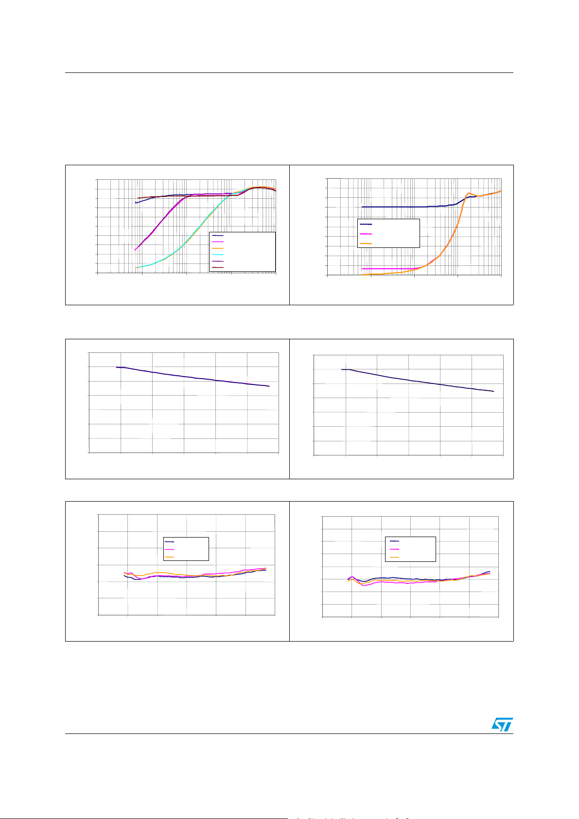
5 Typical operating characteristics
Figure 3. Efficiency vs
100
100
90
90
80
80
70
70
60
60
50
50
40
40
Efficiency (%)
Efficiency (%)
30
30
20
20
10
10
0
0
0.001 0.01 0.1 1 10
0.001 0.01 0.1 1 10
load - 1.5 V and 1.8 V, V
Output current (A)
Output current (A)
= 12 V
IN
DDR2 - Forced PWM
DDR2 - Forced PWM
DDR2 - No-Audible P-S
DDR2 - No-Audible P-S
DDR2 - Pulse-Skip
DDR2 - Pulse-Skip
DDR3 - Forced PWM
DDR3 - Forced PWM
DDR3 - No-Audible P-S
DDR3 - No-Audible P-S
DDR3 - Pulse-Skip
DDR3 - Pulse-Skip
Figure 4. Switching frequency vs
load - 1.8 V, VIN = 12 V
500
500
450
450
400
400
350
350
300
300
250
250
200
200
150
150
100
100
Swiching frequency (kHz)
Swiching frequency (kHz)
50
50
0
0
0.001 0.01 0.1 1 10
0.001 0.01 0.1 1 10
Forced PWM
Forced PWM
No-Audible P-S
No-Audible P-S
Pulse-Skip
Pulse-Skip
Output current (A)
Output current (A)
Figure 5. Switching frequency vs
500
500
450
450
400
400
350
350
300
300
250
250
Switching frequency (kHz)
Switching frequency (kHz)
200
200
150
150
0.0 5.0 10.0 15.0 20.0 25.0 30.0
0.0 5.0 10.0 15.0 20.0 25.0 30.0
Figure 7. VDDQ line regulation, 1.8 V, 7 A Figure 8. VDDQ line regulation, 1.5 V, 7 A
1.8000
1.8000
1.7990
1.7990
1.7980
1.7980
1.7970
1.7970
1.7960
1.7960
Output vol tage (V)
Output vol tage (V)
1.7950
1.7950
1.7940
1.7940
input voltage, 1.8 V
Input voltage (V)
Input voltage (V)
Forced PWM
Forced PWM
No-Audible P-S
No-Audible P-S
Pulse-Skip
Pulse-Skip
0.0 5.0 10.0 15.0 20.0 25.0 30.0
0.0 5.0 10.0 15.0 20.0 25.0 30.0
Input volt age (V)
Input volt age (V)
Figure 6. Switching frequency vs
input voltage, 1.5 V
500
500
450
450
400
400
350
350
300
300
250
250
Switchin g frequency (kHz)
Switchin g frequency (kHz)
200
200
150
150
0.0 5.0 1 0.0 15.0 20.0 25.0 30.0
0.0 5.0 1 0.0 15.0 20.0 25.0 30.0
1.4980
1.4980
1.4975
1.4975
1.4970
1.4970
1.4965
1.4965
1.4960
1.4960
1.4955
1.4955
Output voltag e (V)
Output voltag e (V)
1.4950
1.4950
1.4945
1.4945
1.4940
1.4940
0.0 5.0 10.0 15.0 20.0 25.0 30.0
0.0 5.0 10.0 15.0 20.0 25.0 30.0
Input voltage (V)
Input voltage (V)
Forced PWM
Forced PWM
No-Audible P-S
No-Audible P-S
Pulse-Skip
Pulse-Skip
Input voltage (V )
Input voltage (V )
14/54 Doc ID 14432 Rev 4
Page 15

PM6670S Typical operating characteristics
Figure 9. VDDQ load regulation, 1.8 V,
V
= 12 V
1.860
1.860
1.850
1.850
1.840
1.840
1.830
1.830
1.820
1.820
Output voltage (V)
Output voltage (V)
1.810
1.810
1.800
1.800
0.001 0.01 0.1 1 10
0.001 0.01 0.1 1 10
IN
Forced PWM
Forced PWM
No-Audible P-S
No-Audible P-S
Pulse-Skip
Pulse-Skip
Output current (A)
Output current (A)
Figure 10. VDDQ load regulation, 1.5 V,
V
= 12 V
IN
1.530
1.530
Forced PWM
1.520
1.520
1.510
1.510
1.500
1.500
1.490
1.490
1.480
1.480
Output voltage (V)
Output voltage (V)
1.470
1.470
0.001 0.01 0.1 1 10
0.001 0.01 0.1 1 10
Output current (A)
Output current (A)
Forced PWM
No-Audible P-S
No-Audible P-S
Pulse-Skip
Pulse-Skip
Figure 11. VTT load regulation, 0.9 V,
0.940
0.930
0.920
0.910
0.900
Output volt age (V)
0.890
0.880
LDOIN
-2.5 -1.5 -0.5 0.5 1.5 2.5
= 1.8 V
Output current (A)
Figure 13. VTTREF load regulation, 0.9 V,
VSNS = 1.8 V
Figure 12. VTT load regulation, 0.75 V,
LDOIN = 1.5 V
0.790
0.780
0.770
0.760
0.750
Output voltage (V)
0.740
0.730
-2.5 -1.5 -0.5 0.5 1.5 2.5
Output current (A)
Figure 14. No-audible pulse-skip waveforms
Doc ID 14432 Rev 4 15/54
Page 16

Typical operating characteristics PM6670S
Figure 15. Power-up sequence - AVCC above
UVLO
Figure 17. -1.8 A to 1.8 A VTT
load transient, 0.9 V
Figure 16. VDDQ soft-start, 1.8 V, heavy load
Figure 18. 0 mA to 9 mA VTTREF
load transient, 0.9 V
16/54 Doc ID 14432 Rev 4
Page 17
PM6670S Typical operating characteristics
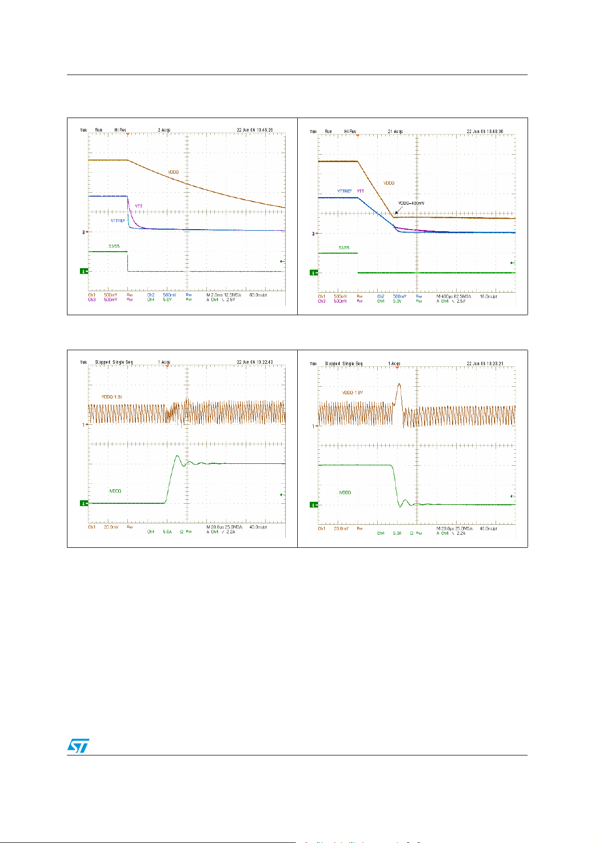
Figure 19. Non-tracking (soft) discharge Figure 20. Tracking (fast) discharge,
LDOIN = VDDQ
Figure 21. 0 A to 10 A VDDQ
load transient, PWM
Figure 22. 10 A to 0 A VDDQ
load transient, PWM
Doc ID 14432 Rev 4 17/54
Page 18

Typical operating characteristics PM6670S
Figure 23. 0 A to 10 A VDDQ
load transient, pulse-skip
Figure 25. Over-voltage protection,
VDDQ = 1.8 V
Figure 24. 10 A to 0 A VDDQ
load transient, pulse-skip
Figure 26. Under-voltage protection,
VDDQ = 1.8 V
18/54 Doc ID 14432 Rev 4
Page 19

PM6670S Block diagram
6 Block diagram
Figure 27. Functional and block diagram
VOSC
1.236V
1.236V
Bandgap
Bandgap
VOSC
Ton
Ton
1-shot
1-shot
Ton
Ton
min
min
1-shot
1-shot
Toff
Toff
min
min
1-shot
1-shot
Anti Cros s
Anti Cros s
Conduction
Conduction
Level
Level
shifter
shifter
Zero Crossing &
Zero Crossing &
Current Limit
Current Limit
BOOT
BOOT
HGATE
HGATE
PHASE
PHASE
VCC
VCC
LGATE
LGATE
PGND
PGND
CSNS
CSNS
VTTSNS
VTTSNS
LDOIN
LDOIN
VTT
VTT
VTTGND
VTTGND
Vr = 0.9V
Vr = 0.9V
NTD
NTD
VREF
VREF
HIZ
HIZ
TD
TD
VTTREF
VTTREF
SGND
SGND
AVCC
AVCC
DDRSEL
DDRSEL
DSCG
DSCG
Table 7. Legend
SWEN Switching controller enable
TD Tracking discharge enable
NTD Non-tracking discharge enable
BEN VTTREF buffer enable
HIZ LDO high impedance mode enable
BEN
BEN
NTD
NTD
UVLO
UVLO
R
R
R
R
UVP/OVP
UVP/OVP
SWEN
SWEN
Thermal Shutdown
Thermal Shutdown
CONTROL LOGIC
CONTROL LOGIC
S3
S3
S5
S5
TD
TD
NTD
NTD
MODE
MODE
BEN
BEN
HIZ
HIZ
Vr
Vr
SWEN
SWEN
_
_
VREF
VREF
+
+
Vr +10
%
Vr +10
%
+
gm
gm
-
-
+
+
DDR3
DDR3
adj
adj
+
Vr
Vr
-
-
+
+
-
-
Vr -10
%
Vr -10
%
NTD
NTD
fix
fix
COMP
COMP
PG
PG
VSNS
VSNS
Doc ID 14432 Rev 4 19/54
Page 20

Device description PM6670S
7 Device description
The PM6670SS is designed to satisfy DDR2-3 power supply requirements combining a
synchronous buck controller, a 15 mA buffered reference and a high-current low-drop out
(LDO) linear regulator capable of sourcing and sinking up to 2 Apk. The switching controller
section is a high-performance, pseudo-fixed frequency, constant-on-time (COT) based
regulator specifically designed for handling fast load transient over a wide range of input
voltages.
The DDR2-3 supply voltage VDDQ can be easily set to 1.8 V (DDR2) or 1.5 V (DDR3)
without additional components. The output voltage can also be adjusted in the 0.9 V to 2.6 V
range using an external resistor divider. The switching mode power supply (SMPS) can
handle different modes of operation in order to minimize noise or power consumption,
depending on the application needs.
A lossless current sensing scheme, based on the Low-Side MOSFET’s on resistance avoids
the need for an external current sense resistor.
The output of the linear regulator (VTT) tracks the memory’s reference voltage VTTREF
within ±30 mV over the full operating load conditions. The input of the LDO can be either
VDDQ or a lower voltage rail in order to reduce the total power dissipation. Linear regulator
stability is achieved by filtering its output with a ceramic capacitor (20 μF or greater).
The reference voltage (VTTREF) section provides a voltage equal to one half of VSNS with
an accuracy of 1 %. This regulator can source and sink up to ±15 mA. A 10 nF to 100 nF
bypass capacitor is required between VTTREF and SGND for stability.
According to DDR2/3 JEDEC specifications, when the system enters the suspend-to-RAM
state the LDO output is left in high impedance while VTTREF and VDDQ are still alive.
When the suspend-to-disk state (S3 and S5 tied to ground) is entered, all outputs are
actively discharged when either tracking or non-tracking discharge is selected.
20/54 Doc ID 14432 Rev 4
Page 21
PM6670S Device description
7.1 VDDQ section - constant on-time PWM controller
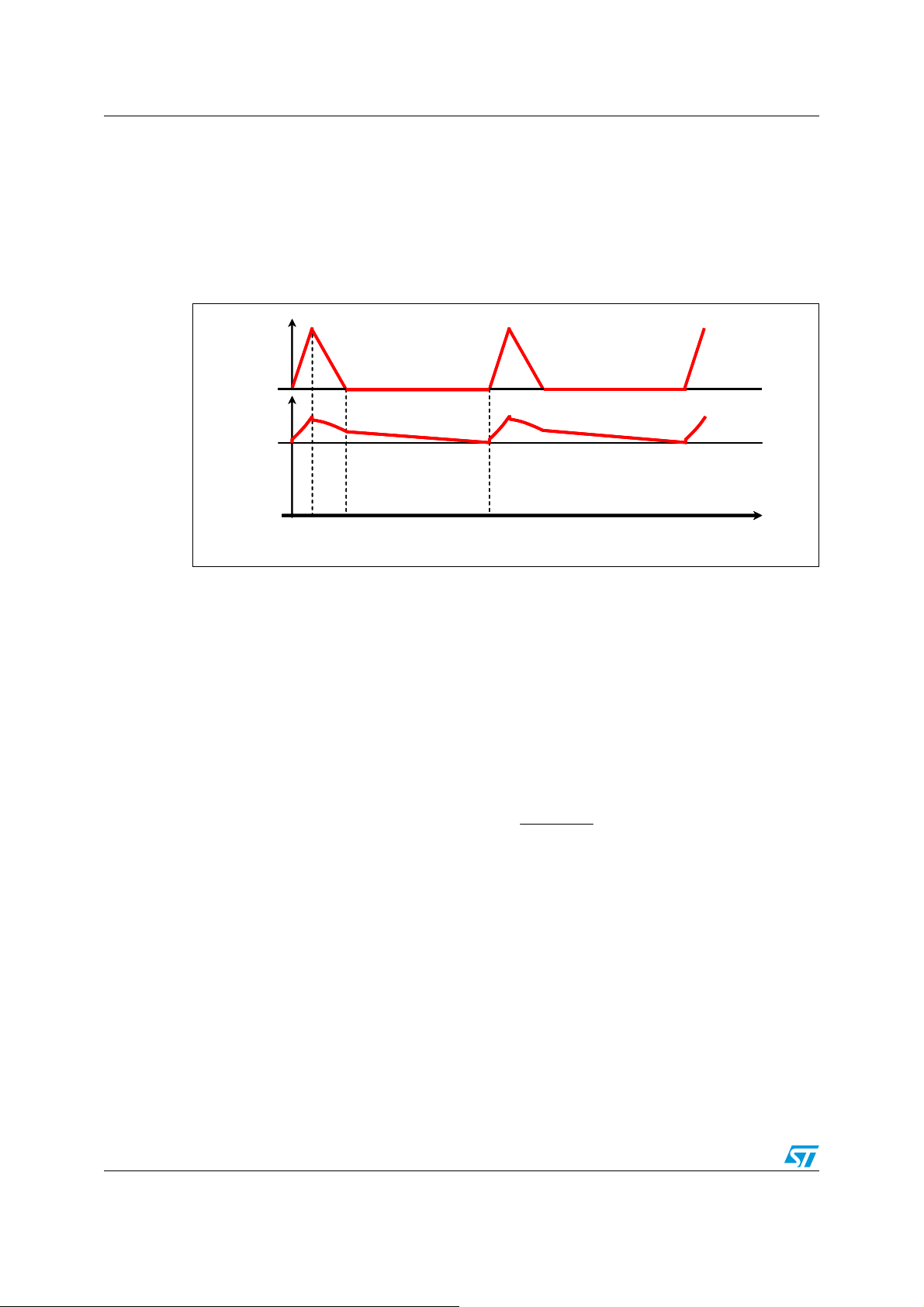
The PM6670S uses a pseudo-fixed frequency, constant on-time (COT) controller as the core
of the switching section. It is well known that the COT controller uses a relatively simple
algorithm and uses the ripple voltage derived across the output capacitor’s ESR to trigger
the on-time one-shot generator. In this way, the output capacitor’s ESR acts as a current
sense resistor providing the appropriate ramp signal to the PWM comparator. Nearly
constant switching frequency is achieved by the system’s loop in steady-state operating
conditions by varying the on-time duration, avoiding thus the need for a clock generator. The
on-time one shot duration is directly proportional to the output voltage, sensed at VSNS pin,
and inversely proportional to the input voltage, sensed at the VOSC pin, as follows:
Equation 1
V
KT
SNS
OSCON
V
τ+=
OSC
where K
is a constant value (130 ns typ.) and τ is the internal propagation delay (40ns
OSC
typ.). The one-shot generator directly drives the high-side MOSFET at the beginning of each
switching cycle allowing the inductor current to increase; after the on-time has expired, an
Off-Time phase, in which the low-side MOSFET is turned on, follows. The off-time duration
is solely determined by the output voltage: when lower than the set value (i.e. the voltage at
VSNS pin is lower than the internal reference V
= 0.9 V), the synchronous rectifier is turned
R
off and a new cycle begins (Figure 28).
Figure 28. Inductor current and output voltage in steady state conditions
Inductor
Inductor
current
current
Output
Output
voltage
voltage
V
reg
V
reg
t
Ton
Ton
Toff
Toff
t
Doc ID 14432 Rev 4 21/54
Page 22

Device description PM6670S
The duty-cycle of the buck converter is, in steady-state conditions, given by
Equation 2
V
OUT
D
--------------=
V
IN
The switching frequency is thus calculated as
Equation 3
V
OUT
SNS
α
OSC
===
α
1
K
OSCOUT
SW
D
T
ON
f ⋅
V
IN
V
K
OSC
V
OSC
where
Equation 4a
V
α
OSC
-------------- -=
OSC
V
IN
Equation 4b
V
α
OUT
--------------=
V
SNS
OUT
Referring to the typical application schematic (figures on cover page and Figure 29), the
final expression is then:
Equation 5
α
f ⋅
SW
OSC
=
K
OSC
R
2
=
RR
+
1
K
OSC21
Even if the switching frequency is theoretically independent from battery and output
voltages, parasitic parameters involved in power path (like MOSFETs' on-resistance and
inductor's DCR) introduce voltage drops responsible for slight dependence on load current.
In addition, the internal delay is due to a small dependence on input voltage. The PM6670S
switching frequency can be set by an external divider connected to the VOSC pin.
Figure 29. Switching frequency selection and VOSC pin
VIN
R1
R2
PM6670
PM6670S
VOSC
The suggested voltage range for VOSC pin is 0.3 V to 2 V, for better switching frequency
programmability.
22/54 Doc ID 14432 Rev 4
Page 23
PM6670S Device description
7.1.1 Constant-on-time architecture
Figure 30 shows the simplified block diagram of the constant-on-time controller.
The switching regulator of the PM6670S owns a one-shot generator that ignites the highside MOSFET when the following conditions are simultaneously satisfied: the PWM
comparator is high (i.e. output voltage is lower than Vr = 0.9 V), the synchronous rectifier
current is below the current limit threshold and the minimum off-time has expired.
A minimum off-time constraint (300 ns typ.) is introduced to assure the boot capacitor
charge and allow inductor valley current sensing on low-side MOSFET. A minimum on-time
is also introduced to assure the start-up switching sequence.
Once the on-time has timed out, the high side switch is turned off, while the synchronous
rectifier is ignited according to the anti-cross conduction management circuitry.
When the output voltage reaches the valley limit (determined by internal reference
Vr = 0.9 V), the low-side MOSFET is turned off according to the anti-cross conduction logic
once again, and a new cycle begins.
Figure 30. Switching section simplified block diagram
Doc ID 14432 Rev 4 23/54
Page 24
Device description PM6670S
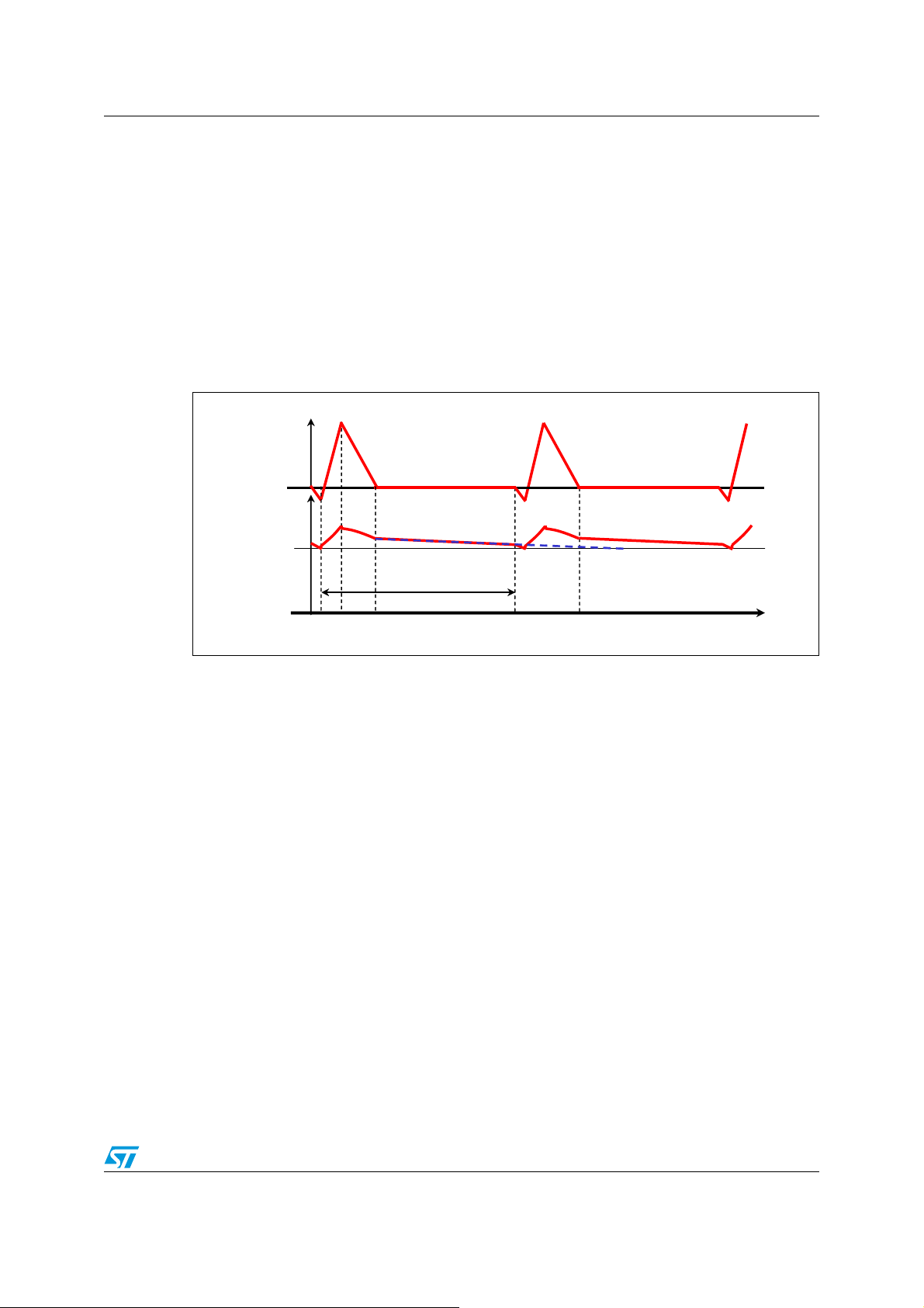
7.1.2 Output ripple compensation and loop stability
The loop is closed connecting the center tap of the output divider (internally, when the fixed
output voltage is chosen, or externally, using the MODE pin in the adjustable output voltage
mode). The feedback node is the negative input of the error comparator, while the positive
input is internally connected to the reference voltage (Vr = 0.9 V). When the feedback
voltage becomes lower than the reference voltage, the PWM comparator goes to high and
sets the control logic, turning on the high-side MOSFET. After the on-time (calculated as
previously described) the system releases the high-side MOSFET and turns on the
synchronous rectifier.
The voltage drop along ground and supply PCB paths, used to connect the output capacitor
to the load, is a source of DC error. Furthermore the system regulates the output voltage
valley, not the average, as shown in
capacitor is an additional source of DC error. To compensate this error, an integrative
network is introduced in the control loop, by connecting the output voltage to the COMP pin
through a capacitor (C
) as shown in Figure 31.
INT
Figure 31. Circuitry for output ripple compensation
COMP PIN
VOLTAGE
Vr
OUTPUT
VOLTAGE
ΔV
t
ΔV
t
Figure 28. Thus, the voltage ripple on the output
REF
V
V
REF
C
C
INT
INT
I=gm(V1-Vr)
Vr
Vr
R
R
Fb2
Fb2
g
m
g
m
+
V
1
V
1
COMP
FILT
C
FILT
C
INT
C
INT
C
V
V
INT
R
INT
R
R
Fb1
R
Fb1
+
-
PWM
Comparator
ESR
ESR
OUT
C
C
OUT
VSNS
The additional capacitor is used to reduce the voltage on the COMP pin when higher than
300 mVpp and is unnecessary for most of applications. The trans conductance amplifier
(gm) generates a current, proportional to the DC error, used to charge the CINT capacitor.
The voltage across the CINT capacitor feeds the negative input of the PWM comparator,
forcing the loop to compensate the total static error. An internal voltage clamp forces the
COMP pin voltage range to ±150 mV with respect to VREF. This is useful to avoid or smooth
output voltage overshoot during a load transient. When the pulse-skip mode is entered, the
clamping range is automatically reduced to 60 mV in order to enhance the recovering
capability. In the ripple amplitude is larger than 150 mV, an additional capacitor CFILT can
be connected between the COMP pin and ground to reduce ripple amplitude, otherwise the
integrator will operate out of its linearity range. This capacitor is unnecessary for most of
applications and can be omitted.
24/54 Doc ID 14432 Rev 4
Page 25

PM6670S Device description
The design of the external feedback network depends on the output voltage ripple. If the
ripple is higher than approximately 20 mV, the correct CINT capacitor is usually enough to
keep the loop stable. The stability of the system depends firstly on the output capacitor zero
frequency.
The following condition must be satisfied:
Equation 6
out
k
ESRC2
⋅⋅π
fkf
=⋅>
ZoutSW
where k is a fixed design parameter (k > 3). It determines the minimum integrator capacitor
value:
Equation 7
g
C
>
INT
2
m
f
⎛
SW
f
−⋅π
⎜
⎝
Zout
k
⎞
⎟
⎠
⋅
Vout
Vr
where gm = 50 μs is the integrator trans conductance.
In order to ensure stability it must be also verified that:
Equation 8
g
C ⋅
INT
m
>
f2
⋅π
Vr
V
OUTZout
If the ripple on the COMP pin is greater than the integrator 150 mV, the auxiliary capacitor
C
can be added. If q is the desired attenuation factor of the output ripple, C
FILT
FILT
is given
by:
Equation 9
C
FILT
In order to reduce the noise on the COMP pin, it is possible to add a resistor R
together with CINT and C
, becomes a low pass filter. The cutoff frequency f
FILT
INT
=
q
that,
INT
must be
CUT
)q1(C
−⋅
much greater (10 or more times) than the switching frequency:
Equation 10
f2
CUT
1
CC
⋅
⋅⋅π
FILTINT
CC
+
FILTINT
R
=
INT
If the ripple is very small (lower than approximately 20 mV), a different compensation
network, called “Virtual-ESR” network, is needed. This additional circuit generates a
triangular ripple that is added to the output voltage ripple at the input of the integrator. The
complete control scheme is shown in
Doc ID 14432 Rev 4 25/54
Figure 32.
Page 26

Device description PM6670S
Figure 32. “Virtual-ESR” network
R
R
T
ΔV
COMP PIN
VOLTAGE
V
REF
t
R
R
R
R
C
C
1
1
INT
INT
ΔV
2
t
REF
V
REF
V
Fb1
R
Fb1
R
+
-
PWM
PWM
Comparator
Comparator
FILT
FILT
I=gm(V1-Vr)
Vr
Vr
m
g
m
g
+
1
V
1
V
R
Fb2
Fb2
R
COMP
COMP
INT
C
INT
C
C
C
VSNS
ESR
ESR
OUT
C
OUT
C
t
T NODE
VOLTAGE
ΔV
1
OUTPUT
VOLTAGE
The ripple on the COMP pin is the sum of the output voltage ripple and the triangular ripple
generated by the Virtual-ESR network. In fact the Virtual-ESR Network behaves like a
another equivalent series resistor R
VESR
.
A good trade-off is to design the network in order to achieve an RVESR given by:
Equation 11
R
VESR
=
where ΔIL is the inductor current ripple and V
greater than approximately 20 mV.
The new closed-loop gain depends on C
INT
that:
Equation 12
C
>
INT
where:
Equation 13
f
=
Z
and:
V
RIPPLE
Δ
RIPPLE
ESR
−
I
L
is the total ripple at the T node, chosen
. In order to ensure stability it must be verified
g
Vr
m
⋅
Vout
f2
⋅π
Z
1
RC2
⋅⋅π
TOTout
26/54 Doc ID 14432 Rev 4
Page 27

PM6670S Device description
Equation 14
R
= ESR + R
TOT
VESR
Moreover, the C
capacitor must meet the following condition:
INT
Equation 15
fkf
=⋅>
ZSW
where R
the Virtual-ESR Network (R
is the sum of the ESR of the output capacitor and the equivalent ESR given by
TOT
). The k parameter must be greater than unity (k > 3) and
VESR
determines the minimum integrator capacitor value C
k
⋅⋅π
RC2
TOTout
:
INT
Equation 16
g
C
>
INT
2
m
f
⎛
SW
−⋅π
⎜
k
⎝
Vr
⋅
Vout
⎞
f
⎟
Z
⎠
The capacitor of the virtual-ESR Network, C, is chosen as follows:
Equation 17
C5C⋅>
INT
and R is calculated to provide the desired triangular ripple voltage:
Equation 18
R
L
=
VESR
CR
⋅
Finally the R1 resistor is calculated according to expression 19:
Equation 19
⎛
⎜
R
⋅
⎜
⎝
1R
=
−
R
⎞
1
⎟
⎟
fC
⋅π⋅
Z
⎠
1
⋅π⋅
fC
Z
Doc ID 14432 Rev 4 27/54
Page 28
Device description PM6670S
⋅
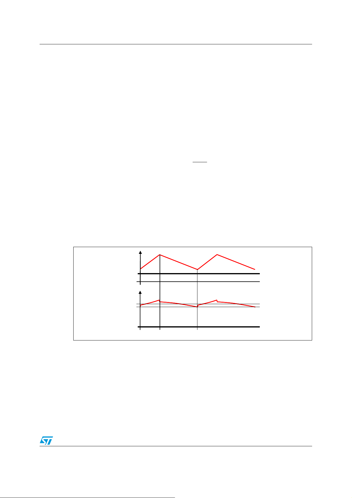
7.1.3 Pulse-skip and no-audible pulse-skip modes
High efficiency at light load conditions is achieved by PM6670S entering the pulse-skip
mode (if enabled). When one of the two fixed output voltages is set, pulse-skip power saving
is a default feature. At light load conditions the zero-crossing comparator truncates the lowside switch on-time as soon as the inductor current becomes negative; in this way the
comparator determines the on-time duration instead of the output ripple (see
Figure 33. Inductor current and output voltage at light load with pulse-skip
Inductor
Inductor
current
current
VDDQ
VDDQ
Output
Output
V
reg
V
reg
T
ON
T
ON
T
OFF
T
OFF
T
IDLE
Figure 33).
t
As a consequence, the output capacitor is left floating and its discharge depends solely on
the current drained from the load. When the output ripple on the pin COMP falls under the
reference, a new shot is triggered and the next cycle begins. The pulse-skip mode is
naturally obtained enabling the zero-crossing comparator and automatically takes part in the
COT algorithm when the inductor current is about half the ripple current amount, i.e.
migrating from continuous conduction mode (C.C.M.) to discontinuous conduction mode
(D.C.M.).
The output current threshold related to the transition between PWM mode and pulse-skip
mode can be approximately calculated as:
Equation 20
VV
−
OUTIN
LOAD
)Skip2PWM(I ⋅
=
T
L2
ON
At higher loads, the inductor current never crosses zero and the device works in pure PWM
mode with a switching frequency around the nominal value.
A physiological consequence of pulse-skip mode is a more noisy and asynchronous (than
normal conditions) output, mainly due to very low load. If the pulse-skip is not compatible
with the application, the PM6670S, when set in adjustable mode-of-operation, allows the
user to choose between forced-PWM and no-audible pulse-skip alternative modes (see
Chapter 7.1.4 on page 30 for details).
28/54 Doc ID 14432 Rev 4
Page 29
PM6670S Device description
No-audible pulse-skip mode
Some audio-noise sensitive applications cannot accept the switching frequency to enter the
audible range as is possible in pulse-skip mode with very light loads. For this reason, the
PM6670S implements an additional feature to maintain a minimum switching frequency of
33 kHz despite a slight efficiency loss. At very light load conditions, if any switching cycle
has taken place within 30 μs (typ.) since the last one (because the output voltage is still
higher than the reference), a no-audible pulse-skip cycle begins. The low-side MOSFET is
turned on and the output is driven to fall until the reference has been crossed. Then, the
high-side switch is turned on for a T
rectifier is enabled until the inductor current reaches the zero-crossing threshold (see
Figure 34).
Figure 34. Inductor current and output voltage at light load with non-audible pulse-skip
Inductor
current
VDDQ
Output
V
reg
period and, once it has expired, the synchronous
ON
T
MAX
TONT
OFF
T
IDLE
t
For frequencies higher than 33 kHz (due to heavier loads) the device works in the same way
as in pulse-skip mode. It is important to notice that in both pulse-skip and no-audible pulseskip modes the switching frequency changes not only with the load but also with the input
voltage.
Doc ID 14432 Rev 4 29/54
Page 30

Device description PM6670S
7.1.4 Mode-of-operation selection
Figure 35. MODE and DDRSEL multifunction pin configurations
VDDQ
VDDQ
R9
R9
R8
R8
+5V
+5V
PM6670
PM6670
PM6670S PM6670S
MODE
MODE
DDRSEL
DDRSEL
(a) (b)
(a) (b)
VDDQ
VDDQ
R9
R9
R8
R8
+5V
+5V
V
REF
V
REF
PM6670
PM6670
MODE
MODE
DDRSEL
DDRSEL
The PM6670S has been designed to satisfy the widest range of applications involving
DDR2/3 memories, SSTL15-18 buses termination and I/O supplies for CPU/chipset. The
device is provided with multilevel pins which allow the user to choose the appropriate
configuration. The MODE pin is used to firstly decide between fixed preset or adjustable
(user defined) output voltages.
When the MODE pin is connected to +5 V, the PM6670S allows setting the VDDQ voltage to
1.8 V or 1.5 V just forcing the DDRSEL multilevel pin to +5 V or to ground respectively (see
Figure 35a).
In this condition the pulse-skip feature is enabled. This device configuration is suitable for
standard DDR2/3 memory supply applications avoiding the need for an external, high
accuracy, divider for output voltage setting.
Applications requiring different output voltages can be managed by PM6670S simply setting
the adjustable mode. If MODE pin voltage is higher than 4 V, the fixed output mode is
selected. Connecting an external divider to the MODE pin (
negative input of the error amplifier and the output voltage is given by expression (21).
Equation 21
ADJ
30/54 Doc ID 14432 Rev 4
Figure 35b), it is used as
9R8R
+
9.0VDDQ
⋅=
8R
Page 31

PM6670S Device description
VDDQ output voltage can be set in the range of 0.9 V to 2.6 V. Adjustable mode
automatically switches DDRSEL pin to become the power saving algorithm selector: if tied
to +5 V, the forced-PWM (fixed frequency) control is performed. If grounded or connected to
VREF pin (1.237 V reference voltage), the pulse-skip or non-audible pulse-skip modes are
respectively selected.
Table 8. Mode-of-operation settings summary
Mode DDRSEL VDDQ Operating mode
V
MODE
> 4.3 V
V
DDRSEL
> 4.2 V 1.8 V
< 3.5 V
DDRSEL
<0.5 V
V
MODE
< 3.7 V
V
1V < V
V
> 4.2 V
DDRSEL
< 3.5 V Non-audible pulse-skip
DDRSEL
< 0.5 V Pulse-skip
DDRSEL
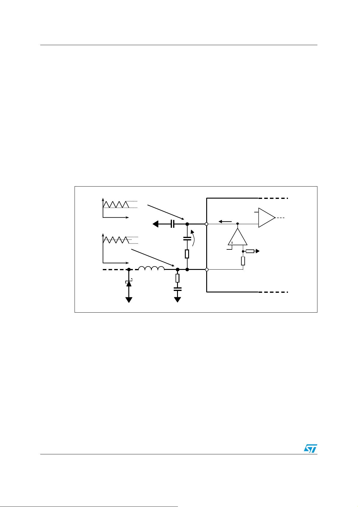
7.1.5 Current sensing and current limit
The PM6670S switching controller uses a valley current sensing algorithm to properly
handle the current limit protection and the inductor current zero-crossing information. The
current is sensed during the conduction time of the low-side MOSFET. The current sensing
element is the on-resistance of the low-side switch. The sensing scheme is visible in
Figure 36.
Figure 36. Current sensing scheme
PM6670
PM6670
PM6670S
PGND
PGND
HGATE
HGATE
PHASE
PHASE
CSNS
CSNS
LGATE
LGATE
100µA·
100µA·
1.5 V
Pulse-skip1V < V
Forced-PWM
ADJ
V
V
IN
IN
V
V
OUT
OUT
R
R
ILIM
ILIM
I
·
R
I
·
R
VALLEY
DSon
VALLEY
DSon
An internal 120 μA current source is connected to C
pin that is also the non-inverting
SNS
input of the positive current limit comparator. When the voltage drop developed across the
sensing parameter equals the voltage drop across the programming resistor R
ILIM
, the
controller skips subsequent cycles until the overcurrent condition is detected or the output
UV protection latches off the device (see
protections on page 36
).
Doc ID 14432 Rev 4 31/54
Section 7.1.11: Over voltage and under voltage
Page 32
Device description PM6670S
Referring to Figure 36, the R
DS(on)
without the need for an external sensing resistor. The on-resistance of the MOSFET is
affected by temperature drift and nominal value spread of the parameter itself; this must be
considered during the R
setting resistor design.
ILIM
It must be taken into account that the current limit circuit actually regulates the inductor
valley current. This means that R
maximum DC output current plus half of the inductor ripple current:
Equation 22
The PM6670S provides also a fixed negative current limit to prevent excessive reverse
inductor current when the switching section sinks current from the load in forced-PWM (3
quadrant working conditions). This negative current limit threshold is measured between
PHASE and PGND pins, comparing the drop magnitude on PHASE pin with an internal
110 mV fixed threshold.
7.1.6 POR, UVLO and soft-start
The PM6670S automatically performs an internal startup sequence during the rising phase
of the analog supply of the device (AVCC). The switching controller remains in a stand-by
state until AVCC crosses the upper UVLO threshold (4.25 V typ.), keeping active the internal
discharge MOSFETs (only if AVCC > 1 V).
sensing technique allows high efficiency performance
must be calculated to set a limit threshold given by the
ILIM
R
ILIM
CL
A120I ⋅μ=
R
DSon
rd
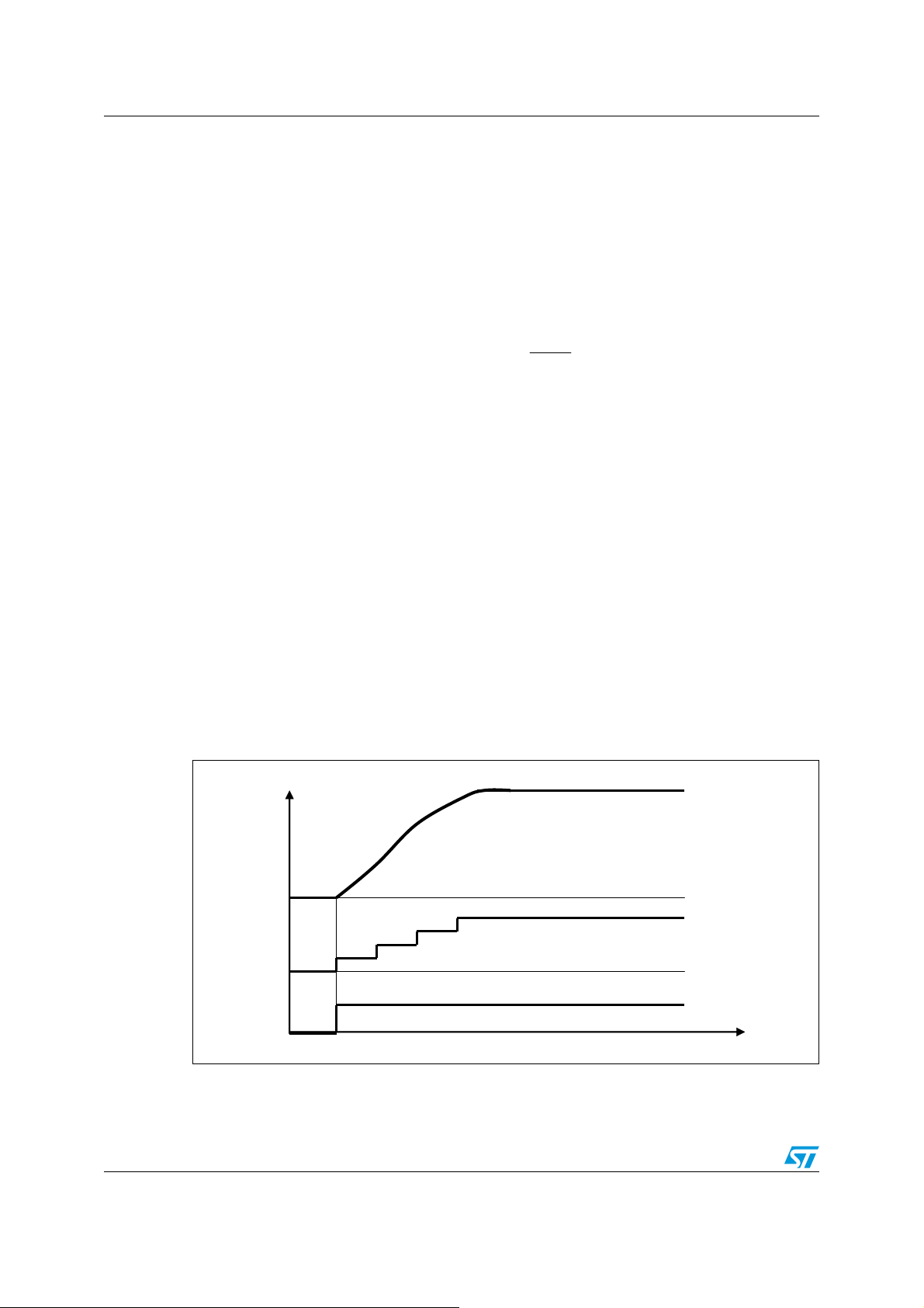
The soft-start allows a gradual increase of the internal current limit threshold during start-up
reducing the input/output surge currents. At the beginning of start-up, the PM6670S current
limit is set to 25 % of nominal value and the under voltage protection is disabled. Then, the
current limit threshold is sequentially brought to 100 % in four steps of approximately 750 μs
(
Figure 37).
Figure 37. Soft-start waveforms
Switching output
Current limit threshold
S5
Time
32/54 Doc ID 14432 Rev 4
Page 33

PM6670S Device description
After a fixed 3 ms total time, the soft-start finishes and UVP is released: if the output voltage
doesn't reach the under voltage threshold within soft-start duration, the UVP condition is
detected and the device performs a soft end and latches off. Depending on the load
conditions, the inductor current may or may not reach the nominal value of the current limit
during the soft-start (
Figure 38. Soft-start at heavy load (a) and short-circuit (b) conditions, pulse-skip enabled
Figure 38 shows two examples).
(a)
7.1.7 Power Good signal
The PG pin is an open drain output used to monitor output voltage through VSNS (in fixed
output voltage mode) or MODE (in adjustable output voltage mode) pins and is enabled
after the soft-start timer has expired. PG signal is held low if the VDDQ output voltage drops
10 % below or rises 10 % above the nominal regulated value. The PG output can sink
current up to 4 mA.
(b)
Doc ID 14432 Rev 4 33/54
Page 34

Device description PM6670S
7.1.8 VDDQ output discharge
Active discharge of VDDQ output occurs when PM6670S enters the suspend-to-disk system
state (S3 and S5 tied to GND) and DSCG pin has been properly set.
Figure 39. DSCG pin connection for discharge mode selection
+5V
+5V
V
REF
V
REF
The PM6670S allows the user to choose between fast discharge (tracking discharge), soft
discharge (non-tracking discharge) or no discharge modes. Voltage on DSCG multilevel pin
determines discharge mode as shown in
Table 9. Discharge mode selection
PM6670S
PM6670
PM6670
DSCG
DSCG
Table 9 on page 34.
DSCG voltage Soft-End type Description
VDSCG > 4.2 V No discharge All outputs left floating.
1 V< VDSCG < 3.5 V Fast (tracking)
VDSCG < 0.5 V Soft (non-tracking) All outputs discharged by dedicated internal MOS.
VDDQ and VTT actively discharged by LDO trough
LDOIN and VTT pins;
Tracking discharge allows the fastest discharge of all outputs but requires the LDOIN to be
self-supplied from VDDQ output voltage. When an external supply rail is connected to
LDOIN, it must be taken into account to avoid damage to the device. Discharge current (1 A)
flows through the LDOIN pin until the output has reached approximately 400 mV and then a
soft discharge completes the process by discharging the output with an internal 22 Ω switch.
Figure 40. Fast discharge and soft discharge options
VDDQ
VDDQ
VTT
VTT
Soft discharge
Soft discharge
400mV
400mV
VDDQ
VDDQ
VTT
VTT
Fast discharge
Fast discharge
Soft discharge
Soft discharge
34/54 Doc ID 14432 Rev 4
Page 35

PM6670S Device description
7.1.9 Gate drivers
The integrated high-current gate drivers allow using different power MOSFETs. The highside driver uses a bootstrap circuit which is supplied by the +5 V rail. The BOOT and
PHASE pins work respectively as supply and return path for the high-side driver, while the
low-side driver is directly fed through VCC and PGND pins.
An important feature of the PM6670S gate drivers is the adaptive anti-cross-conduction
circuitry, which prevents high-side and low-side MOSFETs from being turned on at the same
time. When the high-side MOSFET is turned off, the voltage at the PHASE node begins to
fall. The low-side MOSFET is turned on only when the voltage at the PHASE node reaches
an internal threshold (2.5 V typ.). Similarly, when the low-side MOSFET is turned off, the
high-side one remains off until the LGATE pin voltage is above 1V.
The power dissipation of the drivers is a function of the total gate charge of the external
power MOSFETs and the switching frequency, as shown in the following equation:
Equation 23
fQV)driver(P ⋅⋅=
SWgDRVD
The low-side driver has been designed to have a low-resistance pull-down transistor
(0.6 Ω typ.) in order to prevent undesired ignition of the low-side MOSFET due to the Miller
effect.
7.1.10 Reference voltage and bandgap
The 1.237 V internal bandgap reference has a granted accuracy of ±1 % over the
0 °C to 85 °C temperature range. The VREF pin is a buffered replica of the bandgap voltage.
It can supply up to ±100 μA and is suitable to set the intermediate level of MODE, DDRSEL
and DSCG multifunction pins. A 100 nF (min.) bypass capacitor toward SGND is required to
enhance noise rejection. If VREF falls below 0.8 V (typ.), the system detects a fault condition
and all the circuitry is turned OFF.
An internal divider derives a 0.9 V ± 1 % voltage (Vr) from the bandgap. This voltage is used
as a reference by the switching regulator output. The over-voltage protection, the undervoltage protection and the power good signal are also referred to Vr.
Doc ID 14432 Rev 4 35/54
Page 36

Device description PM6670S
7.1.11 Over voltage and under voltage protections
When the switching output voltage is about 115 % of its nominal value, a latched overvoltage protection (OVP) occurs. In this case the synchronous rectifier immediately turns on
while the high-side MOSFET turns OFF. The output capacitor is rapidly discharged and the
load is preserved from being damaged. The OVP is also active during the soft start. Once
an OVP has occurred, a toggle on S5 pin or a power-on-reset is necessary to exit from the
latched state.
When the switching output voltage is below 70 % of its nominal value, a latched undervoltage protection occurs. This event causes the switching section to be immediately
disabled and both switches to be opened. The controller enters in soft-end mode and the
output is eventually kept to ground, turning the low side MOSFET on when the voltage is
lower than 400 mV. If S3 and S5 are forced low, the low-side MOSFET is released and only
the 22 Ω switch is active.
The under-voltage protection circuit is enabled only at the end of the soft-start. Once an
UVP has occurred, a toggle on S5 pin or a power-on-reset is necessary to clear the fault
state and restart the device.
7.1.12 Device thermal protection
The internal control circuitry of the PM6670S self-monitors the junction temperature and
turns all outputs off when the 150 °C limit has been overrun. This event causes the switching
section to be immediately disabled and both switches to be opened. The controller enters in
Soft-End Mode and the output is eventually kept to ground, turning the low side MOSFET on
when the voltage is lower than 400 mV. If S3 and S5 are forced low, the low-side switch is
released and only the 22 Ω discharge MOSFET is active.
The thermal fault is a latched protection and normal operating condition is restored by a
Power-on reset or toggling S5.
Table 10. OV, UV and OT faults management
Fault Conditions Action
VDDQ over voltage
VDDQ under voltage
Junction over
temperature
VDDQ > 115 % of the
nominal value
VDDQ < 70 % of the
nominal value
> +150 °C
T
J
LGATE pin is forced high and the device latches off.
Exit by a power-on reset or toggling S5
LGATE pin is forced high after the soft-end, then the
device latches off. Exit by a power-on reset or
toggling S5.
LGATE pin is forced high after the soft-end, then the
device latches off. Exit by a power-on reset or
toggling S5 after 15 °C temperature drop.
36/54 Doc ID 14432 Rev 4
Page 37

PM6670S Device description
7.2 VTTREF buffered reference and VTT LDO section
The PM6670S provides the required DDR2/3 reference voltage on the VTTREF pin. The
internal buffer tracks half the voltage on the VSNS pin and has a sink and source capability
up to 15 mA.
Higher currents rapidly deteriorate the output accuracy. A 10 nF to 100 nF (33 nF typ.)
bypass capacitor to SGND is required for stability.
The VTT low-drop-out linear regulator has been designed to sink and source up to 2 A peak
current and 1 A continuously. The VTT voltage tracks VTTREF within ± 35 mV.
A remote voltage sensing pin (VTTSNS) is provided to recovery voltage drops due to
parasitic resistance. In DDR2/3 applications, the linear regulator input LDOIN is typically
connected to VDDQ output; connecting LDOIN pin to a lower voltage, if available in the
system, reduces the power dissipation of the LDO.
A minimum output capacitance of 20 μF (2x10 μF MLCC capacitors) is enough to assure
stability and fast load transient response.
7.2.1 VTT and VTTREF Soft-Start
Soft-Start on VTT and VTTREF outputs is achieved by current clamping.
The LDO linear regulator is provided with a current foldback protection: when the output
voltage exits the internal ±10 % VTT-Good window, the output current is clamped at ±1 A.
Re-entering VTT-Good window releases the current limit clamping.
The foldback mechanism naturally implements a two steps soft-start charging the output
capacitors with a 1 A constant current.
Something similar occurs at VTTREF pin, where the output capacitor is smoothly charged at
a fixed 40 mA current limit.
7.2.2 VTTREF and VTT outputs discharge
The tracking discharge mechanism involves the VTT linear regulator. When the suspend-todisk state is entered, the switching regulator is turned OFF.
At the same time the LDO drains a 1 A constant current from LDOIN and keeps VTT in track
with VTTREF that, in turn, is half the voltage at the VSNS pin. When the VDDQ output
reaches 400 mV, the PM6670S switches on the internal discharge MOSFETs to complete
the process (see
In soft discharge (i.e. non-tracking discharge) the PM6670S disables the internal regulators
and suddenly turns on the discharge MOSFETs on each output.
Section 7.1.8: VDDQ output discharge on page 34).
Doc ID 14432 Rev 4 37/54
Page 38

Device description PM6670S
7.3 S3 and S5 power management pins
According to DDR2/3 memories supply requirements, the PM6670S can manage all S0 to
S5 system states by connecting S3-S5 pins to their respective sleep-mode signals in the
notebook motherboard.
Keeping S3 and S5 high, the S0 (Full-On) state is decoded and the outputs are alive.
In S3 state (S5 = 1, S3 = 0), the PM6670S maintains VDDQ and VTTREF outputs active
and VTT output in high-impedance as needed.
In S4/S5 states (S5 = S3 = 0) all outputs are turned off and, according to DSCG pin voltage,
the proper Soft-End is performed.
Table 11. S3 and S5 sleep-states decoding
S3 S5 System state VDDQ VTTREF VTT
1 1 S0 (full-On) On On On
0 1 S3 (suspend-to-RAM) On On Off (Hi-Z)
0 0 S4/S5 (suspend-to-Disk) Off (discharge) Off (discharge) Off (discharge)
38/54 Doc ID 14432 Rev 4
Page 39

PM6670S Application information
8 Application information
The purpose of this chapter is to show the design procedure of the switching section.
The design starts from three main specifications:
● The input voltage range, provided by the battery or the AC adapter. The two extreme
values (V
● The maximum load current, indicated by I
● The maximum allowed output voltage ripple V
It's also possible that specific designs should involve other specifications.
The following paragraphs will guide the user into a step-by-step design.
8.1 External components selection
The PM6670S uses a pseudo-fixed frequency, constant on-time (COT) controller as the core
of the switching section. The switching frequency can be set by connecting an external
divider to the VOSC pin. The voltage seen at this pin must be greater than 0.8 V and lower
than 2 V in order to ensure system's linearity.
INMAX
and V
) are important for the design.
INmin
LOAD,MAX
RIPPLE,MAX
.
.
Nearly constant switching frequency is achieved by the system's loop in steady-state
operating conditions by varying the on-time duration, avoiding thus the need for a clock
generator. The On-Time one shot duration is directly proportional to the output voltage,
sensed at VSNS pin, and inversely proportional to the input voltage, sensed at the VOSC
pin, as follows:
Equation 24
V
SNS
τ+=
OSC
where K
KT
OSCON
V
is a constant value (130 ns typ.) and τ is the internal propagation delay
OSC
(40 ns typ.).
The duty cycle of the buck converter is, under steady state conditions, given by
Equation 25
V
OUT
D =
V
IN
The switching frequency is thus calculated as
Equation 26
V
OUT
SNS
OSC
α
OSC
=
α
1
K
OSCOUT
f ⋅
D
SW
T
ON
Doc ID 14432 Rev 4 39/54
V
K
OSC
IN
V
⋅
V
==
Page 40

Application information PM6670S
where
Equation 27a
V
OSC
=α
OSC
V
IN
Equation 27b
V
SNS
=α
OUT
V
OUT
Referring to the typical application schematic (figure in cover page and Figure 29), the final
expression is then:
Equation 28
α
f ⋅
SW
OSC
=
K
OSC
R
2
=
RR
+
1
K
OSC21
The switching frequency directly affects two parameters:
● Inductor size: greater frequencies mean smaller inductances. In notebook applications,
real estate solutions (i.e. low-profile power inductors) are mandatory also with high
saturation and r.m.s. currents.
● Efficiency: switching losses are proportional to the frequency. Generally, higher
frequencies imply lower efficiency.
Even if the switching frequency is theoretically independent from battery and output
voltages, parasitic parameters involved in power path (like MOSFETs on-resistance and
inductor DCR) introduce voltage drops responsible for a slight dependence on load current.
In addition, the internal delay is due to a light dependence on input voltage.
Table 12. Typical values for switching frequency selection
R1 (kΩ)R2 (kΩ) Approx switching frequency (kHz)
330 11 250
330 13 300
330 15 350
330 18 400
330 20 450
330 22 500
40/54 Doc ID 14432 Rev 4
Page 41

PM6670S Application information
8.1.1 Inductor selection
Once the switching frequency has been defined, the inductance value depends on the
desired inductor ripple current. Low inductance value means great ripple current that brings
poor efficiency and great output noise. On the other hand a great current ripple is desirable
for fast transient response when a load step is applied.
High inductance brings higher efficiency, but the transient response is critical, especially if
- V
V
INmin
system stability and jitter-free operations (see output capacitor selection paragraph). The
product of the output capacitor's ESR multiplied by the inductor ripple current must be taken
into consideration. A good trade-off between the transient response time, the efficiency, the
cost and the size is choosing the inductance value in order to maintain the inductor ripple
current between 20 % and 50 % (usually 40 %) of the maximum output current.
is small. Moreover a minimum output ripple voltage is necessary to assure
OUT
The maximum inductor ripple current, ΔI
, occurs at the maximum input voltage.
L,MAX
Given these considerations, the inductance value can be calculated with the following
expression:
Equation 29
−
=
L ⋅
where fSW is the switching frequency, VIN is the input voltage, V
is the inductor ripple current.
ΔI
L
V
VV
OUTIN
Δ⋅
OUT
V
Ifsw
IN
L
is the output voltage and
OUT
Once the inductor value is determined, the inductor ripple current is then recalculated:
Equation 30
VV
I ⋅
=Δ
MAX,L
−
Lfsw
⋅
V
OUTMAX,IN
OUT
V
MAX,IN
The next step is the calculation of the maximum r.m.s. inductor current:
Equation 31
2
MAX,L
12
)I(
Δ
2
)I(I
+=
MAX,LOADRMS,L
The inductor must have an r.m.s. current greater than I
in order to assure thermal
L,RMS
stability.
Then the calculation of the maximum inductor peak current follows:
Equation 32
I
Δ
MAX,L
+=
2
I
L,PEAK
II
MAX,LOADPEAK,L
is important in inductor selection in term of its saturation current.
Doc ID 14432 Rev 4 41/54
Page 42

Application information PM6670S
The saturation current of the inductor should be greater than I
saturation core inductors. Using soft-ferrite cores it is possible (but not advisable) to push
the inductor working near its saturation current.
In
Ta bl e 1 3 some inductors suitable for notebook applications are listed.
Table 13. Evaluated inductors (@fsw = 400 kHz)
Manufacturer Series Inductance (µH)
COILCRAFT MLC1538-102 1 13.4 21.0
COILCRAFT MLC1240-901 0.9 12.4 24.5
COILCRAFT MVR1261C-112 1.1 20 20
WURTH 7443552100 1 16 20
COILTRONICS HC8-1R2 1.2 16.0 25.4
In pulse-skip mode, low inductance values produce a better efficiency versus load curve,
while higher values result in higher full-load efficiency because of the smaller current ripple.
8.1.2 Input capacitor selection
In a buck topology converter the current that flows through the input capacitor is pulsed and
with zero average value. The RMS input current can be calculated as follows:
L,PEAK
+40 °C rms
current (A)
not only in case of hard
-30 % saturation
current (A)
Equation 33
Cin
RMS
LOAD
2
1
)D1(DII Δ⋅+−⋅⋅=
12
2
)I(D
L
Neglecting the second term, the equation 10 is reduced to:
Equation 34
)D1(DII
Cin
RMS
LOAD
−⋅=
The losses due to the input capacitor are thus maximized when the duty-cycle is 0.5:
Equation 35
CinRMSCinloss
2
LOADCin
The input capacitor should be selected with a RMS rated current higher than I
2
(max))I5.0(ESR(max)IESRP ⋅⋅=⋅=
CINRMS
(max).
Tantalum capacitors are good in terms of low ESR and small size, but they occasionally can
burn out if subjected to very high current during operation. Multi-layers-ceramic-capacitors
(MLCC) have usually a higher RMS current rating with smaller size and they remain the best
choice. The drawback is their quite high cost.
42/54 Doc ID 14432 Rev 4
Page 43

PM6670S Application information
It must be taken into account that in some MLCC the capacitance decreases when the
operating voltage is near the rated voltage. In
Ta bl e 1 4 some MLCC suitable for most of
applications are listed.
Table 14. Evaluated MLCC for input filtering
Manufacturer Series Capacitance (μF) Rated voltage (V)
TAIYO YUDEN UMK325BJ106KM-T 10 50 2
TAIYO YUDEN GMK316F106ZL-T 10 35 2.2
TAIYO YUDEN GMK325F106ZH-T 10 35 2.2
TAIYO YUDEN GMK325BJ106KN 10 35 2.5
TDK C3225X5R1E106M 10 25
8.1.3 Output capacitor selection
Using tantalum or electrolytic capacitors, the selection is made referring to ESR and voltage
rating rather than by a specific capacitance value.
The output capacitor has to satisfy the output voltage ripple requirements. At a given
switching frequency, small inductor values are useful to reduce the size of the choke but
increase the inductor current ripple. Thus, to reduce the output voltage ripple a low ESR
capacitor is required.
To reduce jitter noise between different switching regulators in the system, it is preferable to
work with an output voltage ripple greater than 25 mV.
As far as it concerning the load transient requirements, the equivalent series resistance
(ESR) of the output capacitor must satisfy the following relationship:
Maximum Irms
@100 kHz (A)
Equation 36
where V
ESRΔ≤
is the maximum tolerable ripple voltage.
RIPPLE
V
MAX,RIPPLE
I
MAX,L
In addition, the ESR must be high enough high to meet stability requirements. The output
capacitor zero must be lower than the switching frequency:
Equation 37
ff
=>
ZSW
Doc ID 14432 Rev 4 43/54
1
CESR2
⋅⋅π
out
Page 44
Application information PM6670S
⋅
If ceramic capacitors are used, the output voltage ripple due to inductor current ripple is
negligible. Then the inductance could be smaller, reducing the size of the choke. In this case
it is important that output capacitor can adsorb the inductor energy without generating an
over-voltage condition when the system changes from a full load to a no load condition.
The minimum output capacitance can be chosen by the following equation:
Equation 38
where Vf is the output capacitor voltage after the load transient, while VI is the output
capacitor voltage before the load transient.
Ta bl e 1 5 are listed some tested polymer capacitors are listed.
In
Table 15. Evaluated output capacitors
Manufacturer Series
4TPE220MF 220 4V 15 to 25
SANYO
HITACHI TNCB OE227MTRYF 220 2.5V 25
4TPE150MI 220 4V 18
4TPC220M 220 4V 40
8.1.4 MOSFETs selection
In a notebook application, power management efficiency is a high level requirement. Power
dissipation on the power switches becomes an important factor in the selection of switches.
Losses of high-side and low-side MOSFETs depend on their working condition.
C
IL
=
min,OUT
Capacitance
(μF)
2
MAX,LOAD
22
ViVf
−
Rated voltage
(V)
ESR max @100 kHz
(mΩ)
Considering the high-side MOSFET, the power dissipation is calculated as:
Equation 39
Maximum conduction losses are approximately given by:
Equation 40
RP ⋅⋅=
DSonconduction
V
44/54 Doc ID 14432 Rev 4
V
OUT
min.IN
PPP +=
switchingconductionDHighSide
I
2
MAX,LOAD
Page 45

PM6670S Application information
Δ
≅
−
=
where R
is the drain-source on-resistance of the control MOSFET.
DSon
Switching losses are approximately given by:
Equation 41
Δ
I
L
⋅⋅
ft)
where t
P
switching
ON
and t
=
LOADIN
are the turn-on and turn-off times of the MOSFET and depend on the
OFF
2
2
−⋅
(max)I(V
gate-driver current capability and the gate charge Q
low R
. Unfortunately low R
DSon
As general rule, the R
DSon
x Q
MOSFETs have a great gate charge.
DSon
product should be minimized to find out the suitable
gate
(max)I(V
LOADINswon
+
. A greater efficiency is achieved with
gate
I
L
+⋅
2
⋅⋅
ft)
swoff
2
MOSFET.
Logic-level MOSFETs are recommended, as long as low-side and high-side gate drivers are
powered by V
= +5 V. The breakdown voltage of the MOSFETs (V
VCC
greater than the maximum input voltage.V
INmax
.
BRDSS
) must be
Ta bl e 1 6 lists tested high-side MOSFETs.
Table 16. Evaluated high-side MOSFETs
Manufacturer Type
R
DSon
(mΩ)
Gate charge
(nC)
Rated reverse
voltage (V)
ST STS12NH3LL 10.5 12 30
IR IRF7811 9 18 30
In buck converters the power dissipation of the synchronous MOSFET is mainly due to
conduction losses:
Equation 42
PP
conductionDLowSide
Maximum conduction losses occur at the maximum input voltage:
Equation 43
V
⎞
OUT
⎟
I
⎟
MAX,IN
⎠
as possible. When the high-side
DSon
2
MAX,LOAD
⎛
⎜
1RP ⋅
DSonconduction
−⋅=
⎜
V
⎝
The synchronous rectifier should have the lowest R
MOSFET turns on, high d
through its gate-drain capacitance C
of the phase node can bring up even the low-side gate
V/dt
, causing a cross-conduction problem. Once again,
RRS
the choice of the low-side MOSFET is a trade-off between on resistance and gate charge; a
/ C
good selection should minimize the ratio C
RSS
GS
where
Equation 44
CCC
RSSISSGS
Doc ID 14432 Rev 4 45/54
Page 46

Application information PM6670S
Tested low-side MOSFETs are listed in Tab le 1 7 .
Table 17. Evaluated low-side MOSFETs
Manufacturer Type R
ST STS12NH3LL 13.5 0.069 30
ST STS25NH3LL 4.0 0.011 30
IR IRF7811 24 0.054 30
Dual N-MOS can be used in applications with lower output current.
Ta bl e 1 8 shows some suitable dual MOSFETs for applications requiring about 3 A.
Table 18. Suitable dual MOSFETs
Manufacturer Type R
ST STS8DNH3LL 25 10 30
IR IRF7313 46 33 30
8.1.5 Diode selection
A rectifier across the synchronous switch is recommended. The rectifier works as a voltage
clamp across the synchronous rectifier and reduces the negative inductor swing during the
dead time between turning the high-side MOSFET off and the synchronous rectifier on.
Moreover it increases the efficiency of the system.
Choose a schottky diode as long as its forward voltage drop is very little (0.3 V). The reverse
voltage should be greater than the maximum input voltage V
reverse charge is preferable.
(mΩ) CGD \ C
DSon
(mΩ) Gate charge (nC) Rated reverse voltage (V)
DSon
GS
Rated reverse voltage (V)
and a minimum recovery
INmax
Ta bl e 1 9 shows some evaluated diodes.
Table 19. Evaluated recirculation rectifiers
Manufacturer Type
ST STPS1L30M 0.34 30 0.00039
ST STPS1L30A 0.34 30 0.00039
46/54 Doc ID 14432 Rev 4
Forward
voltage (V)
Rated reverse
voltage (V)
Reverse current (μA)
Page 47

PM6670S Application information
⋅
8.1.6 VDDQ current limit setting
The valley current limit is set by R
current. The valley of the inductor current I
and must be chosen to support the maximum load
CSNS
Lvalley
is:
Equation 45
LOADLvalley
2
Δ
I
L
−=
(max)II
The output current limit depends on the current ripple as shown in Figure 41:
Figure 41. Valley current limit waveforms
Current
Inductor current
MAX LOAD 1
Valley current limit
Inductor current
MAX LOAD 2
Time
As the valley threshold is fixed, the greater the current ripple, the greater the DC output
current will be. If an output current limit greater than I
(max) over all the input voltage
LOAD
range is required, the minimum current ripple must be considered in the previous formula.
Then the resistor R
CSNS
is:
Equation 46
IR
LvalleyDSon
uA100
calculation (typically +0.4 %/°C).
DSon
where R
R
is the drain-source on-resistance of the low-side switch. Consider the
DSon
CSNS
=
temperature effect and the worst case value in R
The accuracy of the valley current also depends on the offset of the internal comparator
(±6 mV).
The negative valley-current limit (if the device works in forced-PWM mode) is given by:
Equation 47
I =
NEG
R
mV110
DSon
Doc ID 14432 Rev 4 47/54
Page 48

Application information PM6670S
8.1.7 All ceramic capacitors application
Design of external feedback network depends on the output voltage ripple across the output
capacitors' ESR. If the ripple is great enough (at least 20 mV), the compensation network
simply consists of a C
Figure 42. Integrative compensation
capacitor.
INT
Ton One-shot
generator
VSNS
VDDQ
+
PWM
Comparator
VREF
-
+
COMP
Integrator
C
FILT
R
INT
The stability of the system depends firstly on the output capacitor zero frequency. It must be
verified that:
C
INT
g
m
-
Vr=0.9
Equation 48
fkf
=⋅>
ZoutSW
where k is a free design parameter greater than unity (k > 3). It determines the minimum
integrator capacitor value C
INT
:
Equation 49
g
>
C
INT
2
48/54 Doc ID 14432 Rev 4
m
f
⎛
SW
⎜
k
⎝
k
CR2
⋅π
outout
Vref
⋅
Vo
⎞
−⋅π
f
⎟
Zout
⎠
Page 49

PM6670S Application information
If the ripple on pin COMP is greater than the integrator output dynamic (150 mV), an
additional capacitor C
could be added in order to reduce its amplitude. If q is the desired
filt
attenuation factor of the output ripple, select:
Equation 50
−⋅
INT
=
C
filt
)q1(C
q
In order to reduce noise on pin COMP, it's possible to introduce a resistor R
with C
INT
and C
, becomes a low pass filter. The cutoff frequency f
filt
CUT
that, together
INT
must be much
greater (10 or more times) than the switching frequency of the section:
Equation 51
1
CC
⋅
⋅π
f2
CUT
FILTINT
CC
+
FILTINT
are unnecessary.
For most of applications both R
R
INT
=
INT
and C
filt
If the ripple is very small (e.g. such as with ceramic capacitors), an additional compensation
network, called “Virtual ESR” network, is needed. This additional part generates a triangular
ripple that substitutes the ESR output voltage ripple. The complete compensation scheme is
represented in
Figure 43.
Figure 43. Virtual ESR network
L
R R1
CINT
VDDQ
C
Ton
Generation
Block
PWM Comparator
+
g
RINT
+
-
VREF
Doc ID 14432 Rev 4 49/54
CFILT
m
Integrator
-
0.9V
Page 50

Application information PM6670S
Select C as shown:
Equation 52
C5C⋅>
INT
Then calculate R in order to have enough ripple voltage on the integrator input:
Equation 53
L
=
VESR
CR
⋅
Where R
R
is the new virtual output capacitor ESR. A good trade-off is to consider an
VESR
equivalent ESR of 30-50 mΩ, even though the choice depends on inductor current ripple.
Then choose R1 as follows:
Equation 54
⎞
⎛
1
⎟
⎜
⋅
R
=
1R
R
⎟
⎜
π
fC
Z
⎠
⎝
1
−
π
fC
Z
50/54 Doc ID 14432 Rev 4
Page 51

PM6670S Package mechanical data
9 Package mechanical data
In order to meet environmental requirements, ST offers these devices in different grades of
®
ECOPACK
packages, depending on their level of environmental compliance. ECOPACK®
specifications, grade definitions and product status are available at: www.st.com. ECOPACK
is an ST trademark.
Table 20. VFQFPN-24 4 mm x 4 mm mechanical data
mm.
Dim.
Min Typ Max
A 0.80 0.90 1.00
A1 0.0 0.05
A2 0.65 0.80
D 4.00
D1 3.75
E4.00
E1 3.75
θ
P 0.24 0.42 0.60
e0.50
12°
N 24.00
Nd 6.00
Ne 6.00
L 0.30 0.40 0.50
b 0.18 0.30
D2 2.40 2.70
E2 2.40 2.70
Doc ID 14432 Rev 4 51/54
Page 52

Package mechanical data PM6670S
Figure 44. Package dimensions
52/54 Doc ID 14432 Rev 4
Page 53

PM6670S Revision history
10 Revision history
Table 21. Document revision history
Date Revision Changes
06-Feb-2008 1 Initial release
23-Feb-2009 2 Updated Table 3 on page 8
30-Oct-2009 3 Updated package drawing in cover page, Table 20 on page 51
03-Feb-2010 4
Updated Table 2 on page 6, Table 6 on page 10, Section 7.1 on page
21, Figure 30 on page 23 and Section 7.1.5 on page 31.
Doc ID 14432 Rev 4 53/54
Page 54

PM6670S
Please Read Carefully:
Information in this document is provided solely in connection with ST products. STMicroelectronics NV and its subsidiaries (“ST”) reserve the
right to make changes, corrections, modifications or improvements, to this document, and the products and services described herein at any
time, without notice.
All ST products are sold pursuant to ST’s terms and conditions of sale.
Purchasers are solely responsible for the choice, selection and use of the ST products and services described herein, and ST assumes no
liability whatsoever relating to the choice, selection or use of the ST products and services described herein.
No license, express or implied, by estoppel or otherwise, to any intellectual property rights is granted under this document. If any part of this
document refers to any third party products or services it shall not be deemed a license grant by ST for the use of such third party products
or services, or any intellectual property contained therein or considered as a warranty covering the use in any manner whatsoever of such
third party products or services or any intellectual property contained therein.
UNLESS OTHERWISE SET FORTH IN ST’S TERMS AND CONDITIONS OF SALE ST DISCLAIMS ANY EXPRESS OR IMPLIED
WARRANTY WITH RESPECT TO THE USE AND/OR SALE OF ST PRODUCTS INCLUDING WITHOUT LIMITATION IMPLIED
WARRANTIES OF MERCHANTABILITY, FITNESS FOR A PARTICULAR PURPOSE (AND THEIR EQUIVALENTS UNDER THE LAWS
OF ANY JURISDICTION), OR INFRINGEMENT OF ANY PATENT, COPYRIGHT OR OTHER INTELLECTUAL PROPERTY RIGHT.
UNLESS EXPRESSLY APPROVED IN WRITING BY AN AUTHORIZED ST REPRESENTATIVE, ST PRODUCTS ARE NOT
RECOMMENDED, AUTHORIZED OR WARRANTED FOR USE IN MILITARY, AIR CRAFT, SPACE, LIFE SAVING, OR LIFE SUSTAINING
APPLICATIONS, NOR IN PRODUCTS OR SYSTEMS WHERE FAILURE OR MALFUNCTION MAY RESULT IN PERSONAL INJURY,
DEATH, OR SEVERE PROPERTY OR ENVIRONMENTAL DAMAGE. ST PRODUCTS WHICH ARE NOT SPECIFIED AS "AUTOMOTIVE
GRADE" MAY ONLY BE USED IN AUTOMOTIVE APPLICATIONS AT USER’S OWN RISK.
Resale of ST products with provisions different from the statements and/or technical features set forth in this document shall immediately void
any warranty granted by ST for the ST product or service described herein and shall not create or extend in any manner whatsoever, any
liability of ST.
ST and the ST logo are trademarks or registered trademarks of ST in various countries.
Information in this document supersedes and replaces all information previously supplied.
The ST logo is a registered trademark of STMicroelectronics. All other names are the property of their respective owners.
© 2010 STMicroelectronics - All rights reserved
STMicroelectronics group of companies
Australia - Belgium - Brazil - Canada - China - Czech Republic - Finland - France - Germany - Hong Kong - India - Israel - Italy - Japan -
Malaysia - Malta - Morocco - Philippines - Singapore - Spain - Sweden - Switzerland - United Kingdom - United States of America
www.st.com
54/54 Doc ID 14432 Rev 4
 Loading...