


Monolithic VR for chipset and DDR2/3 supply
for ultra-mobile PC (UMPC) applications
Features
■ 0.8 V ±1% internal voltage reference
■ 2.7 V to 5.5 V input voltage range
■ Fast response, constant frequency,
current mode control
■ Three independent, adjustable, out-of-phase
SMPS for DDR2/3 (VDDQ) and chipset supply
■ Low noise DDR2/3 reference (VTTREF)
■ ±2 Apk LDO for DDR2/3 termination (VTT)
with foldback
■ S0-S5 states compliant DDR2/3 section
■ Active soft-end for all outputs
■ Selectable tracking discharge for VDDQ
■ Separate Power Good signals
■ Pulse skipping at light load
■ Programmable current limit and soft-start for
all outputs
■ Latched OVP, UVP protection
■ Thermal protection
PM6641
VFQFPN-48 7x7 mm
Description
The PM6641 is a monolithic voltage regulator
module specifically designed to supply DDR2/3
memory and chipset in ultra-mobile PC and real
estate constrained portable systems.
It integrates three independent, adjustable,
constant frequency buck converters, a ±2 Apk low
drop-out (LDO) linear regulator and a
±15 mA low noise buffered reference.
Each regulator provides basic UV and OV
protections, programmable soft-start and current
limit and active soft-end.
Applications
Pulse-skipping technique is performed to increase
efficiency at very light load.
■ DDR2/3 memory and chipset supply
■ UMPC and portable equipment
■ Handheld and PDAs
Table 1. Device summary
Order codes Package Packaging
PM6641
VFQFPN-48 7x7 (exposed pad)
PM6641TR Tape and reel
May 2009 Doc ID 13510 Rev 3 1/47
Tr ay
www.st.com
47

Contents PM6641
Contents
1 Typical application circuit . . . . . . . . . . . . . . . . . . . . . . . . . . . . . . . . . . . . 3
2 Pin settings . . . . . . . . . . . . . . . . . . . . . . . . . . . . . . . . . . . . . . . . . . . . . . . . 4
2.1 Connections . . . . . . . . . . . . . . . . . . . . . . . . . . . . . . . . . . . . . . . . . . . . . . . . 4
2.2 Pin description . . . . . . . . . . . . . . . . . . . . . . . . . . . . . . . . . . . . . . . . . . . . . . 5
3 Electrical data . . . . . . . . . . . . . . . . . . . . . . . . . . . . . . . . . . . . . . . . . . . . . . 7
3.1 Maximum rating . . . . . . . . . . . . . . . . . . . . . . . . . . . . . . . . . . . . . . . . . . . . . 7
3.2 Thermal data . . . . . . . . . . . . . . . . . . . . . . . . . . . . . . . . . . . . . . . . . . . . . . . 7
3.3 Recommended operating conditions . . . . . . . . . . . . . . . . . . . . . . . . . . . . . 8
4 Electrical characteristics . . . . . . . . . . . . . . . . . . . . . . . . . . . . . . . . . . . . . 9
5 Typical operating characteristics . . . . . . . . . . . . . . . . . . . . . . . . . . . . . 13
6 Block diagram . . . . . . . . . . . . . . . . . . . . . . . . . . . . . . . . . . . . . . . . . . . . . 17
7 Device description . . . . . . . . . . . . . . . . . . . . . . . . . . . . . . . . . . . . . . . . . 18
7.1 Memory supply . . . . . . . . . . . . . . . . . . . . . . . . . . . . . . . . . . . . . . . . . . . . 19
7.1.1 VDDQ switching regulator . . . . . . . . . . . . . . . . . . . . . . . . . . . . . . . . . . 19
7.1.2 VTT LDO and VTTREF buffered reference . . . . . . . . . . . . . . . . . . . . . . 20
7.1.3 VTT and VTTREF soft-start . . . . . . . . . . . . . . . . . . . . . . . . . . . . . . . . . 20
7.1.4 S3 and S5 power management pins . . . . . . . . . . . . . . . . . . . . . . . . . . . 21
7.2 Chipset supply . . . . . . . . . . . . . . . . . . . . . . . . . . . . . . . . . . . . . . . . . . . . . 21
7.3 SW regulators control loop . . . . . . . . . . . . . . . . . . . . . . . . . . . . . . . . . . . . 23
7.4 SW regulators pulse skipping and PWM mode . . . . . . . . . . . . . . . . . . . . 25
7.5 Output voltage divider . . . . . . . . . . . . . . . . . . . . . . . . . . . . . . . . . . . . . . . 26
7.6 Outputs soft-start . . . . . . . . . . . . . . . . . . . . . . . . . . . . . . . . . . . . . . . . . . . 27
7.7 Outputs soft-end . . . . . . . . . . . . . . . . . . . . . . . . . . . . . . . . . . . . . . . . . . . . 28
7.8 Switching frequency selection . . . . . . . . . . . . . . . . . . . . . . . . . . . . . . . . . 28
7.9 Phase management . . . . . . . . . . . . . . . . . . . . . . . . . . . . . . . . . . . . . . . . . 29
7.10 Peak current limit . . . . . . . . . . . . . . . . . . . . . . . . . . . . . . . . . . . . . . . . . . . 30
7.11 Fault management . . . . . . . . . . . . . . . . . . . . . . . . . . . . . . . . . . . . . . . . . . 32
2/47 Doc ID 13510 Rev 3

PM6641 Contents
7.11.1 Output overvoltage . . . . . . . . . . . . . . . . . . . . . . . . . . . . . . . . . . . . . . . . . 32
7.11.2 Output under voltage . . . . . . . . . . . . . . . . . . . . . . . . . . . . . . . . . . . . . . . 32
7.11.3 Thermal shutdown . . . . . . . . . . . . . . . . . . . . . . . . . . . . . . . . . . . . . . . . . 33
7.11.4 Input under voltage lock-out . . . . . . . . . . . . . . . . . . . . . . . . . . . . . . . . . . 33
8 Components selection . . . . . . . . . . . . . . . . . . . . . . . . . . . . . . . . . . . . . . 34
8.1 Inductor selection . . . . . . . . . . . . . . . . . . . . . . . . . . . . . . . . . . . . . . . . . . . 34
8.2 Input capacitor selection . . . . . . . . . . . . . . . . . . . . . . . . . . . . . . . . . . . . . . 35
8.3 Output capacitor selection . . . . . . . . . . . . . . . . . . . . . . . . . . . . . . . . . . . . 36
8.4 SW regulator compensation components selection . . . . . . . . . . . . . . . . . 37
8.5 Layout guidelines . . . . . . . . . . . . . . . . . . . . . . . . . . . . . . . . . . . . . . . . . . . 39
9 Application examples . . . . . . . . . . . . . . . . . . . . . . . . . . . . . . . . . . . . . . . 40
9.1 UMPC DDR2 and chipset power supply . . . . . . . . . . . . . . . . . . . . . . . . . 40
10 Package mechanical data . . . . . . . . . . . . . . . . . . . . . . . . . . . . . . . . . . . . 43
11 Revision history . . . . . . . . . . . . . . . . . . . . . . . . . . . . . . . . . . . . . . . . . . . 45
Doc ID 13510 Rev 3 3/47

Typical application circuit PM6641
V
V
V
V
V
V
1 Typical application circuit
Figure 1. Application circuit
1.5
PG_1S5
VTTREF
TT
VIN_1S5
VTTREF
SET_SWF
EN_VTT (S3)
VTTFB
VTT
VTTGND
AVCC
VCC
LDOIN
VIN_1S8
3.3V
1.05
EN_1S5
SS_1S8
PG_1S5
AGND
VIN_1S05
SW_1S05
VFB_1S05
SGND_1S05
SS_1S05
SET_PH1
COMP_1S05
EN_1S05
EN_1S8 (S5)
PG_1S05
PG_1S8
AGND
3.3V
PG_1S05
3.3V
PG_1S8
SW_1S5
VFB_1S5
SGND_1S5
COMP_1S5
SS_1S5
PM6641
VOUT_1S8
VFB_1S8
SGND_1S8
COMP_1S8
CSNS
VSW_1S8
3.3V
5V
1.8
4/47 Doc ID 13510 Rev 3

PM6641 Pin settings
2 Pin settings
2.1 Connections
Figure 2. Pin connection (through top view)
DSCG
VTTREF
LDOIN
VCC
VTTFB
VTT
AGND
SET_SWF
VOUT_1S8
CSNS
SGND_1S8
SGND_1S8
PM6641
VSW_1S8
VSW_1S8
VIN_1S8
VIN_1S8
VFB_1S8
COMP_1S8
VSW_1S05
SGND_1S05
SGND_1S05
VFB_1S05
COMP_1S05
SS_1S05
SS_1S8
VTTGND
AVCC
AGND
SET_PH1
AGND
EN_1S8 (S5)
EN_VTT (S3)
EN_1S5
EN_1S05
VIN_1S5
VSW_1S5
VSW_1S5
SGND_1S5
SGND_1S5
VFB_1S5
COMP_1S5
SS_1S5
PG_1S5
PG_1S05
PG_1S8
VIN_1S05
VIN_1S05
VSW_1S05
Doc ID 13510 Rev 3 5/47

Pin settings PM6641
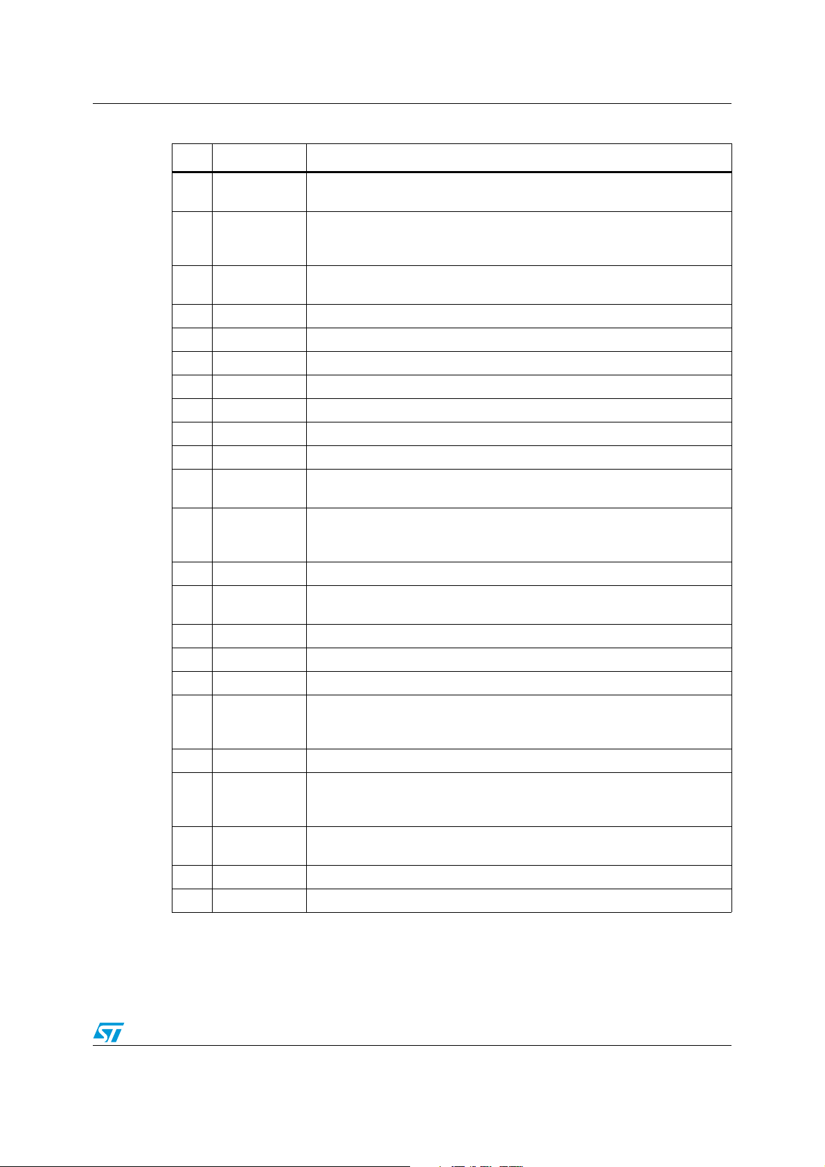
2.2 Pin description
Table 2. Pin functions
n° Pin Function
1 AGND Analog and signal ground.
2 SET_SWF
3 VOUT_1S8 VDDQ/2 divider input and discharge path for 1.8 V rail.
4CSNS
5 SGND_1S8 Switcher power ground for 1.8 V rail.
6 SGND_1S8 Switcher power ground for 1.8 V rail.
7 VSW_1S8 Switch node for 1.8 V rail.
8 VSW_1S8 Switch node for 1.8 V rail.
9 VIN_1S8 Power supply input for 1.8 V rail.
10 VIN_1S8 Power supply input for 1.8 V rail.
11 VFB_1S8
12 COMP_1S8
13 SS_1S8
Switching frequency setting input.
See Chapter 7.8: Switching frequency selection on page 29
Current limit setting input for all rails.
See Chapter 7.10: Peak current limit on page 31
Feedback input for 1.8 V rail.
See Chapter 7.5: Output voltage divider on page 27
Loop compensation output for 1.8 V rail. See Chapter 7.3: SW regulators
control loop on page 24 and Chapter 8.4: SW regulator compensation
components selection on page 38 sections for details.
Positive terminal of the external soft-start capacitor for 1.8 V rail.
See Chapter 7.6: Outputs soft-start on page 28 section for details.
14 SS_1S05
Positive terminal of the external soft-start capacitor for 1.05 V rail.
See Chapter 7.6: Outputs soft-start on page 28 section for details.
Loop compensation output for 1.05 V rail. See Chapter 7.3: SW regulators
15 COMP_1S05
control loop on page 24 and Chapter 8.4: SW regulator compensation
components selection on page 38 for details.
16 VFB_1S05
Feedback input for 1.05 V rail.
See Chapter 7.5: Output voltage divider on page 27 section for details
17 SGND_1S05 Switcher power ground for 1.05 V rail.
18 SGND_1S05 Switcher power ground for 1.05 V rail.
19 VSW_1S05 Switch node for 1.05 V rail.
20 VSW_1S05 Switch node for 1.05 V rail.
21 VIN_1S05 Power supply input for 1.05 V rail.
22 VIN_1S05 Power supply input for 1.05 V rail.
23 PG_1S05
24 PG_1S8
25 PG_1S5
Power Good signal for 1.05 V rail. Open drain. See Chapter 7.2: Chipset
supply on page 22 section for details.
Power Good signal for 1.8 V rail. Open drain. See Chapter 7.1.1: VDDQ
switching regulator on page 20 section for details.
Power Good signal for 1.5 V rail. Open drain. See Chapter 7.2: Chipset
supply on page 22 section for details.
6/47 Doc ID 13510 Rev 3
PM6641 Pin settings
Table 2. Pin functions (continued)
n° Pin Function
26 SS_1S5
Positive terminal of the external soft-start capacitor for 1.5 V rail.
See Chapter 7.6: Outputs soft-start on page 28 section for details.
Loop compensation output for 1.5 V rail. Chapter 7.3: SW regulators control
27 COMP_1S5
loop on page 24 and Chapter 8.4: SW regulator compensation components
selection on page 38 sections for details.
28 VFB_1S5
Feedback input for 1.5 V rail.
See Chapter 7.5: Output voltage divider on page 27 section for details
29 SGND_1S5 Switcher power ground for 1.5 V rail.
30 SGND_1S5 Switcher power ground for 1.5 V rail.
31 VSW_1S5 Switch node for 1.5 V rail.
32 VSW_1S5 Switch node for 1.5 V rail.
33 VIN_1S5 Power supply input for 1.5 V rail.
34 EN_1S05 Enable input for 1.05 V rail.
35 EN_1S5 Enable input for 1.5 V rail.
36 EN_VTT
Enable input for VTT rail. High in S0 system states. See Chapter 7.1.4: S3
and S5 power management pins on page 22 section for details.
Enable input for 1.8 V (VDDQ) rail. High in S0-S3 system states.
37 EN_1S8
See Chapter 7.1.4: S3 and S5 power management pins on page 22 section
for details.
38 AGND Analog and signal ground.
39 SET_PH1
Switching regulator phase control.
See Chapter 7.9: Phase management on page 30 section for details.
40 AGND Analog and signal ground.
41 AVCC Analog circuitry supply. Connect to +5 V by a simple RC filter.
42 VTTGND LDO linear regulator power ground.
LDO linear regulator output. DDR2-3 termination voltage. See Chapter 7.1:
43 VTT
Memory supply on page 20 and Chapter 7.1.2: VTT LDO and VTTREF
buffered reference on page 21 sections for details.
44 LDOIN LDO linear regulator input. Typically connected to the 1.8 V rail.
Reference voltage buffer output. See Chapter 7.1: Memory supply on
45 VTTREF
page 20 and Chapter 7.1.2: VTT LDO and VTTREF buffered reference on
page 21 sections for details.
46 DSCG
Tracking/non-tracking discharge selection for DDR2-3 section. See
Chapter 7.7: Outputs soft-end on page 29 section for details.
47 VTTFB Feedback input for VTT linear regulator output.
48 VCC +5 V switching circuitry supply. Bypass to AGND by a 100 nF capacitor.
Doc ID 13510 Rev 3 7/47
Electrical data PM6641
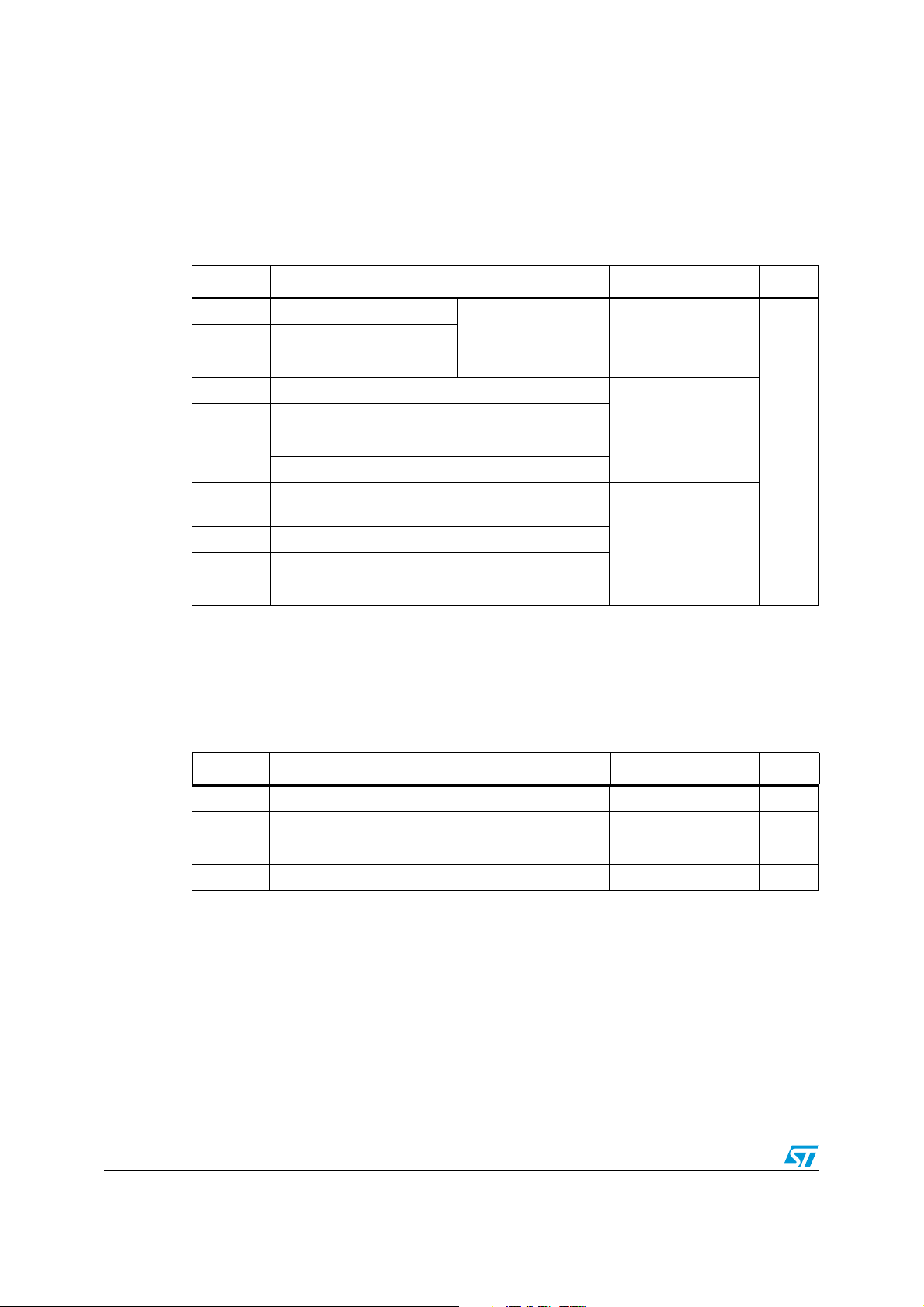
3 Electrical data
3.1 Maximum rating
Table 3. Absolute maximum ratings
(1)
Symbol Parameter Value Unit
V
V
V
VIN
VCC
AVC C
VIN_x to SGND_x
VCC to AGND or SGND_x
AVCC to AGND or SGND_x
V
V
IN
VCC
= V
= V
AVC C
AVC C
-0.3 to 6
AGND to SGND_x
-0.3 to 0.3
VTTGND to SGND_x
VSW_x to SGND_x
V
VSW
VSW_x to AGND
-0.3 to 6
CSNS, PG_x, EN_x, DSCG, COMP_x, VFB_x, SS_x,
SET_SWF, SET_PH1, VOUT_1S8 to AGND
VTT, VTTREF, VTTFB to AGND
-0.3 to V
AVC C
+ 0.3
LDOIN, VTT, VTTREF, VTTFB to VTTGND
P
TOT
1. Free air operating conditions unless otherwise specified. Stresses beyond those listed under “absolute
maximum ratings” may cause permanent damage to the device. Exposure to absolute maximum rated
conditions for extended periods may affect device reliability.
Power dissipation @ TA = 25 °C 4 W
V
3.2 Thermal data
Table 4. Thermal data
Symbol Parameter Value Unit
R
thJA
T
STG
T
A
T
J
Thermal resistance junction to ambient 25 °C/W
Storage temperature range -50 to 150 °C
Operating ambient temperature range -40 to 85 °C
Junction operating temperature range -40 to 125 °C
8/47 Doc ID 13510 Rev 3
PM6641 Electrical data
3.3 Recommended operating conditions
Table 5. Recommended operating conditions
Val ues
Symbol Parameter
Min Typ Max
Unit
V
AVC C
VCC
V
IN
AVCC voltage range 4.5 5.5
VCC IC supply voltage 4.5 V
VIN_x input voltage range 2.7 V
AVC C
VCC
VV
Doc ID 13510 Rev 3 9/47
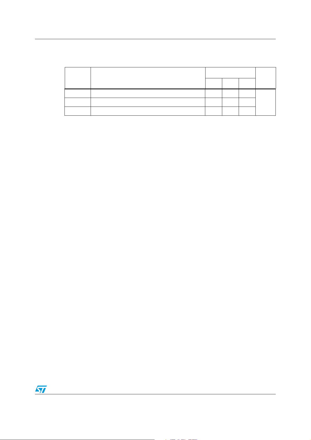
Electrical characteristics PM6641
4 Electrical characteristics
TA = 0 °C to 85 °C, AVCC = 5 V, VCC = 5 V, VIN_x = 3.3 V and LDOIN connected to 1.8 V
output if not otherwise specified
Table 6. Electrical characteristics
Symbol Parameter Test condition
Supply section all rails
I
CC
I
SHDN
UVLO
Error amplifier, FB
V
REF
I
FB
I
SS
Oscillator frequency
AVCC+VCC operating current
Total shutdown current into
VIN_x + AVCC + VCC pins
AVCC under voltage lockout
upper threshold
AVCC under voltage lockout
th
lower threshold
UVLO hysteresis 100 mV
AND SS – all rails
Error amplifier reference voltage V
FB input bias current VFB_X = 0.8 V 25 nA
Soft-start current VSS_X = 0.4 V 10 μA
(a)
.
= +5 V, all switching
V
VCC
regulators active without load
= V
V
IN
AVC C
= V
VCC
all EN_x low
AVC C
= V
= 5 V 792 800 808 mV
VCC
= +5 V,
Val ues
Unit
Min Typ Max
3mA
10 μA
4.0 4.1 4.35
V
3.6 3.9 4.0
R
SETSWF
f
SW
Switching frequency
R
SETSWF
Comp all rails
g
m
COMP_x transconductance 300 µS
UVP/OVP protections and PGOOD signal (SMPS only) all rails
OVP
UVP
Overvoltage threshold 116 120 124
th
Undervoltage threshold 56 60 64
th
Power good upper threshold 106 110 115
PG
th
Power Good lower threshold 86 90 94
I
PG,LEAK
V
PG,LOW
PG_x outputs leakeage current PG_x tied to +5 V 1 µA
PG_x outputs low level V
a. All parameters at operating temperature extremes are guaranteed by design and statistical analysis
(not production tested).
FB_X
10/47 Doc ID 13510 Rev 3
= 140 kΩ 500
= 70 kΩ 1000
= 0.6 V or 1V, I
= 2 mA 250 mV
PG_X
kHzSET_SWF to VCC 675 750 825
%
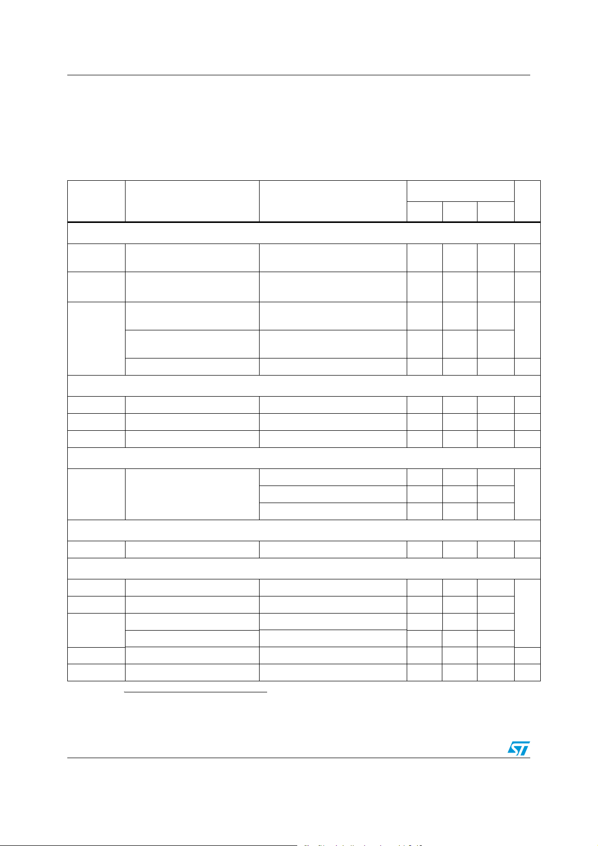
PM6641 Electrical characteristics
Table 6. Electrical characteristics (continued)
Val ues
Symbol Parameter Test condition
Min Typ Max
Thermal shutdown
Unit
T
SHDN
Thermal shutdown hysteresis 15
Switching node – chipset 1.5 V rail
Thermal shutdown threshold 150
t
Onmin
Minimum on-time 200 ns
RDSon,HS High side PMOS Ron 150 220
RDSon,LS Low side NMOS Ron 100 160
=
V
IN
I
INLEAK
VIN_1S5 leakage current
V
EN_1S5 low
Peak current limit R
Soft-end section – chipset 1.5 V rail
Discharge resistance 25 Ω
LS turn-on VFB_1SX threshold
with internal divider
LS turn-on VFB_1SX threshold
with external divider
VFB_S1X to OUT_X 0.29
VFB_S1X to external divider 0.16
Power management section – chipset 1.5 V rail
AVC C
CSNS
= V
= +5 V, all
VCC
= 50 kΩ 3.9 A
+5 V
=
V
IN
+3.3 V
°C
mΩ
1 μA
V
EN_1S5 turn-off level
EN_1S5 turn-on level 2
Switching node – chipset 1.05 V rail
t
Onmin
Minimum on-time 180 ns
RDSon,HS High side PMOS Ron 100 160
RDSon,LS Low side NMOS Ron 70 110
I
INLEAK
Soft end section – chipset 1.05 V rail
VIN_1S05 leakage current
Peak current limit R
Discharge resistance 25 Ω
V
= 5 V
AVC C
mΩ
0.8
=
V
IN
= V
V
AVC C
VCC
EN_1S05 low
= +5 V, all
+5 V
V
IN
=
+3.3 V
= 50 kΩ 5.1 A
CSNS
1
1
Doc ID 13510 Rev 3 11/47
V
μA

Electrical characteristics PM6641
Table 6. Electrical characteristics (continued)
Val ues
Symbol Parameter Test condition
Min Typ Max
Unit
LS turn-on VFB_1SX threshold
with internal divider
LS turn-on VFB_1SX threshold
with external divider
VFB_S1X to OUT_X 0.2
VFB_S1X to external divider 0.16
Power management section – chipset 1.05 V rail
EN_1S05 turn-off level
= +5 V
V
EN_1S05 turn-on level 2
AVC C
0.8
Switching node – DDR2/3 rails
t
Onmin
Minimum on-time 200 ns
RDSon,HS High side PMOS Ron 90 130
RDSon,LS Low side NMOS Ron 80 120
VIN =
I
INLEAK
VIN_1S8 leakage current
Peak current limit R
Soft-end section – DDR2/3 rails
VDDQ discharge resistance in
non-tracking discharge mode
VTTREF discharge resistance
in non-tracking discharge mode
V
AVC C
= V
VCC
= 5 V,
all EN_1S8 low
= 50 kΩ 6.1 A
CSNS
+5 V
V
IN
+3.3 V
=
25 Ω
200 Ω
V
V
mΩ
1
μA
1
VTTFB discharge resistance in
non-tracking discharge mode
V
tracking/Non-tracking discharge
threshold for final
FB_1SX
VFB_S1X to OUT_X 0.340 V
transition with internal divider
V
tracking/Non-tracking discharge
threshold for final
FB_1SX
VFB_S1X to external divider 0.160 V
transition with external divider
Power management section – DDR2/3 rails
DSCG turn-off level
V
DSCG turn-on level 3.5
AVC C
EN_1S8 (S5), EN_VTT (S3)
Turn-Off Level
EN_1S8 (S5), EN_VTT (S3)
V
AVC C
Turn-On Level
12/47 Doc ID 13510 Rev 3
= +5 V
= +5 V
0.8
40 Ω
1.5
V
2
PM6641 Electrical characteristics
Table 6. Electrical characteristics (continued)
Val ues
Symbol Parameter Test condition
Min Typ Max
VTT LDO section – DDR2/3 rails
Unit
PG_VTT_TH
Power Good lower threshold 86 90 94 %
Power Good upper threshold 106 110 114 %
I
LDOIN,ON
LDOIN,STR
I
LDOIN,STD
I
VTTFB, BIAS
VTTFB, LEAK
I
VTT,LEAK
LDO input bias current in fullON state
LDO input bias current in
suspend-to-RAM state
LDO input bias current in
suspend-to-disk state
VTTFB bias current
VTTFB leakage current
VTT leakage current
LDO linear regulator output
voltage (DDR2)
LDO linear regulator output
voltage (DDR3)
V
VTT
LDO output accuracy respect to
VTTREF, V
LDOIN
LDO source current limit
I
VTT,CL
LDO sink current limit
VTTREF section – DDR2/3 rails
=1.8 V
EN_1S8 = EN_VTT = +5 V,
no load on VTT
EN_1S8 = +5 V, EN_VTT = 0 V,
no load on VTT
EN_1S8 = EN_VTT = 0 V,
no load on VTT
EN_1S8 = EN_VTT = +5 V,
V
VTTFB
= V
VOUT_1S8
/2
EN_1S8 = +5 V, EN_VTT = 0 V,
V
VTTFB
= V
VOUT_1S8
/2
EN_1S8 = +5 V, EN_VTT = 0 V,
V
VTT
= V
VOUT _1S8
/2
EN_1S8 = EN_VTT = +5 V,
I
VTT
0 A, V
LDOIN
= 1.8 V
EN_1S8 = EN_VTT = +5 V,
I
VTT
= 0 A, V
LDOIN
= 1.5 V
EN_1S8 = EN_VTT = +5 V,
-1 mA < I
VTT
< 1 mA
EN_1S8 = EN_VTT = +5 V,
-1 A < I
VTT
< 1 A
EN_1S8 = EN_VTT = +5 V,
-2 A < I
V
VTT
V
VTT
V
VTT
V
VTT
< 2 A
VTT
< 1.10*(V
> 1.10*(V
> 0.90*(V
< 0.90*(V
VOUT _1S8
VOUT _1S8
VOUT _1S8
VOUT _1S8
/2) 2 2.3 3
/2) 1 1.25 1.5
/2) -3 -2.3 -2
/2) -1.5 -1.25 -1
110
10
3
1
1
-10 10
0.9
0.75
-20 20
-25 25
-35 35
μAI
μAI
V
mV
A
VTTREF output voltage I
V
VTTREF
I
VTTREF
VTTREF output voltage
accuracy relative to
V
VOUT _1S8
/2
VTTREF short circuit source
current
VTTREF short circuit sink
current
-15 mA < I
V
V
V
VTTREF
VOUT _1S8
VOUT _1S8
VOUT _1S8
= 0A, V
VTTREF
= 1.8 V
= 1.8 V, V
= 1.8 V, V
VOUT _1S8
< +15 mA,
VTTREF
VTTREF
= 1.8 V 0.9 V
-2 2 %
= 0 V 40
mA
= 1.8 V -40
Doc ID 13510 Rev 3 13/47
Typical operating characteristics PM6641
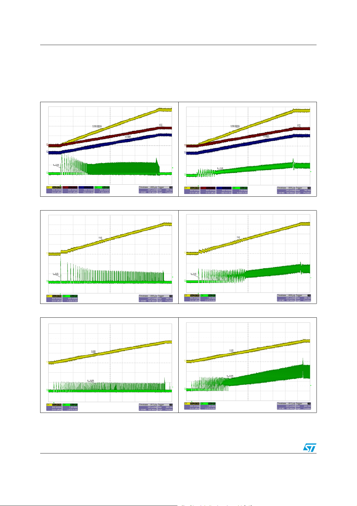
5 Typical operating characteristics
Figure 3. VDDQ and VTT soft-start
Figure 5. 1V5 soft-start without load Figure 6. 1V5 soft-start with load
without load
Figure 4. VDDQ and VTT soft-start with AVG
load
Figure 7. 1V05 soft-start without load Figure 8. 1V05 soft-start without load
14/47 Doc ID 13510 Rev 3
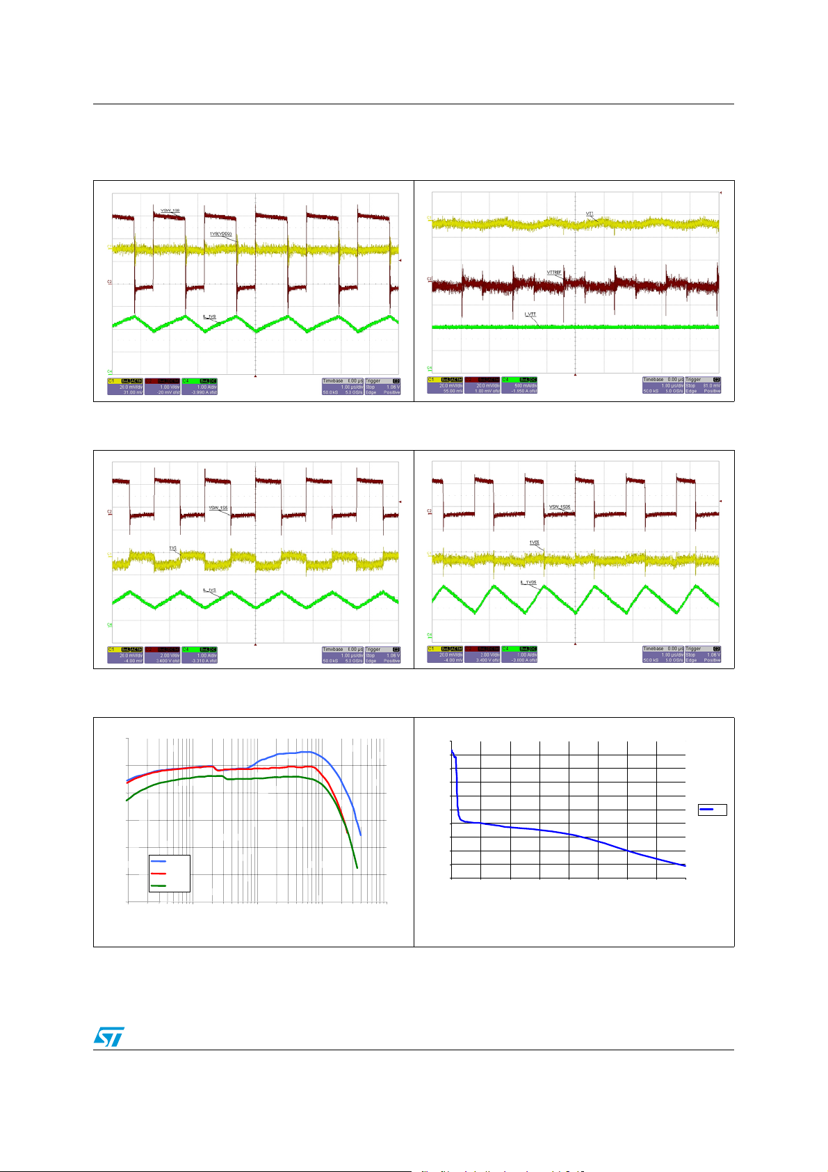
PM6641 Typical operating characteristics
Figure 9. VDDQ output ripple and phase @
AVG current
Figure 10. VTT, VTTREF output ripple @ AVG
current
Figure 11. 1V5 output ripple and phase @
AVG current
Figure 13. SW reg. efficiency @ VIN = 3.3 V,
F
= 600 kHz
1V8
1V8
1V5
1V5
1V05
1V05
SW
Load Current [A]
Load Current [A]
95
95
90
90
85
85
80
80
Efficiency %
Efficiency %
75
75
70
70
65
65
1,0E-03 1,0E-02 1,0E-01 1,0E+00 1,0E+01
1,0E-03 1,0E-02 1,0E-01 1,0E+00 1,0E+01
Figure 12. 1V05 output ripple and phase @
AVG current
Figure 14. VDDQ (1.8 V) load regulation
1,808
1,806
1,804
1,802
1,800
1,798
1,796
1,794
Output voltage (V)
1,792
1,790
1,788
0,00 0,50 1,00 1,50 2,00 2,50 3,00 3,50 4,00
Load Current [A]
1V8
Doc ID 13510 Rev 3 15/47
 Loading...