

2 to 4-cell Li-Ion, Li-FePO4 battery charger with SMBus
interface, N-channel RBFET and BATFET MOSFET selectors
Features
■ Buck converter
– Synchronous buck converter with
N-channel high-side, low-side power
MOSFET integrated drivers
– 350 kHz or 700 kHz switching frequency,
selectable with SMBus
– AC adapter input voltage range 9 V - 24 V
– 5 V bias input voltage supply
– Battery charge voltage range 2.5 V -18 V
– ±0.5% charge voltage accuracy
– 0.1% cell charge voltage resolution
– ±3% charge current accuracy
– ±3% input current accuracy
– Overvoltage, overcurrent protection
– Battery, inductor, power MOSFET short-
circuit protection
– Internal loop compensation network
– Integrated soft-start
■ Selector
– N-channel ACFET/RBFET MOSFET driver
– N-channel BATFET MOSFET driver
■ System
– 1 mA quiescent supply current
– 17 µA - 35 µA sleep mode current (BATFET
charge pump off - on)
– Thermal shutdown
Applications
■ Mobile PC:
– UMPC/MID and tablets
– Netbook and notebook computers
PM6613N
Data brief
QFN3x3 20L
a synchronous switching DC-DC converter with
N-channel high-side and low-side Power
MOSFET drivers. The possibility to set the
switching frequency with SMBus by choosing one
of the two preset values of 350 kHz or 700 kHz
assures the best trade-off between power
conversion efficiency and PCB cost and size.
Integrated loop compensation network and softstart allow the reduction of the number of external
components.
The PM6613N integrates 2 charge pumps to drive
N-channel ACFET/RBFET and BATFET
MOSFETs.
The SMBus communication interface is used to
set the battery charge current and voltage.
The PM6613N charges 2 to 4 series Li-Ion or
LiFePO
available in a compact QFN20L 3x3 mm,
package.
Table 1. Device summary
cells, for mobile PC applications. It is
4
Order code Package Packing
PM6613N QFN3x3 20L Tape and reel
Description
The PM6613N is a high efficiency battery charger
with SMBus communication interface. It includes
February 2012 Doc ID 022741 Rev 1 1/8
For further information contact your local STMicroelectronics sales office.
www.st.com
8
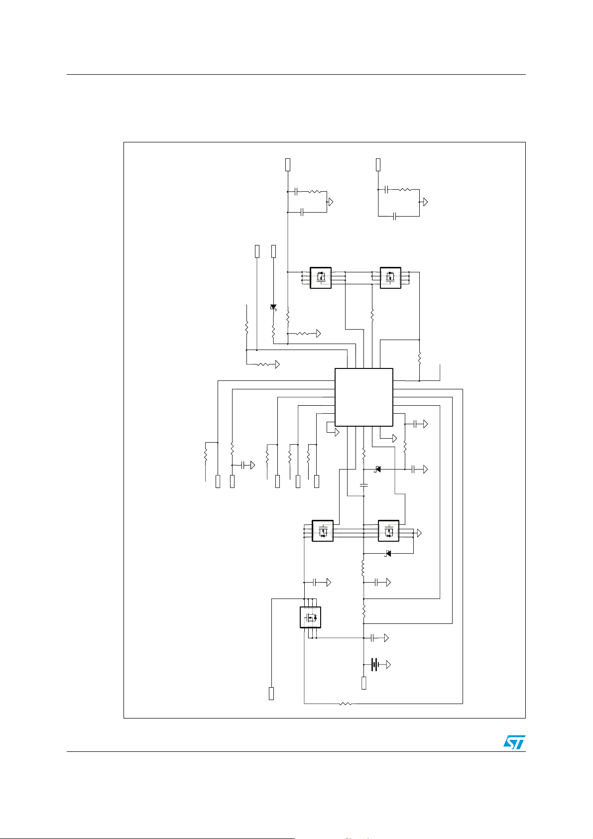
Typical application circuit PM6613N
1 Typical application circuit
Figure 1. Typical application circuit
ADP
RFLT1
3.9R
CADP0
2.2uF ; 25V
CADP1
22uF
WAKE
ILIMex t
WAKE
+5V
D2 BAT54JFILM
RILU
1MR
ACOK
IOUT
10kR
RIOUT
100nF
1MR
RACOKU
+5V
CIOUT
ACOK
IOUT_FLT
RACDIVU
110k R
RWAKE
NM
RILL
ALARM
10kR
RALARMU
+5V
ALARM#
SYS
ACFET
1
8
2
7
3
6
nMOS
STL56N3LLH5
56kR
RACDIVL
SDA
10kR
RSDAU
+5V
SDA
STL56N3LLH5
nMOS
6
7
8
22uF
CIN1
6
7
8
nMOS
234
1
45
B2BC
ILIM
15
ILIM
ACOK
16
IOUT
17
ALARM#
18
SCL
19
SDA
20
THP
PH1HIGH
21
PH
HIGH
45
3
2
1
HS
STL56N3LLH5
ADP
430kR
SCL
10kR
RSCLU
+5V
SCL
5
BATFET
BATFETG
ACDIV
14
2
ACDIV
CBT
L1
RSB
RACDVR
B2B
13
B2B
PM6613N
BTST3LOW4GND
RBT 0R
BTST
220nF
PH
4.7uH
10mR
COUT2
BATT
RBFETG
ACDRV
12
LOW
+
+5V
+5V
2.2uF; 10V
CIN05
C5V
STL56N3LLH5
1
2
3
nMOS
4 5
RBFET
3.9kR
ACP
11
ACP
ACN
ACDR V
BATFET
SRN
SRP
DCIN
5
GND
D1
BAT54JFILM
STL56N3LLH5
nMOS
6
7
8
LS
STPS2L30A
10uF
COUT1
10uF
3.9R
RFLT2
10uF
8
7
6
RSA
10mR
SYS
ACN
10
9
8
7
6
10uF
CDC
1R
RDC
+5V
1uF
CBT1
LSG
45
3
2
1
D3
SRN
SRP
BATFET
SYS
2/8 Doc ID 022741 Rev 1
3.9kR
RBATFET
BATT
AM10245v1
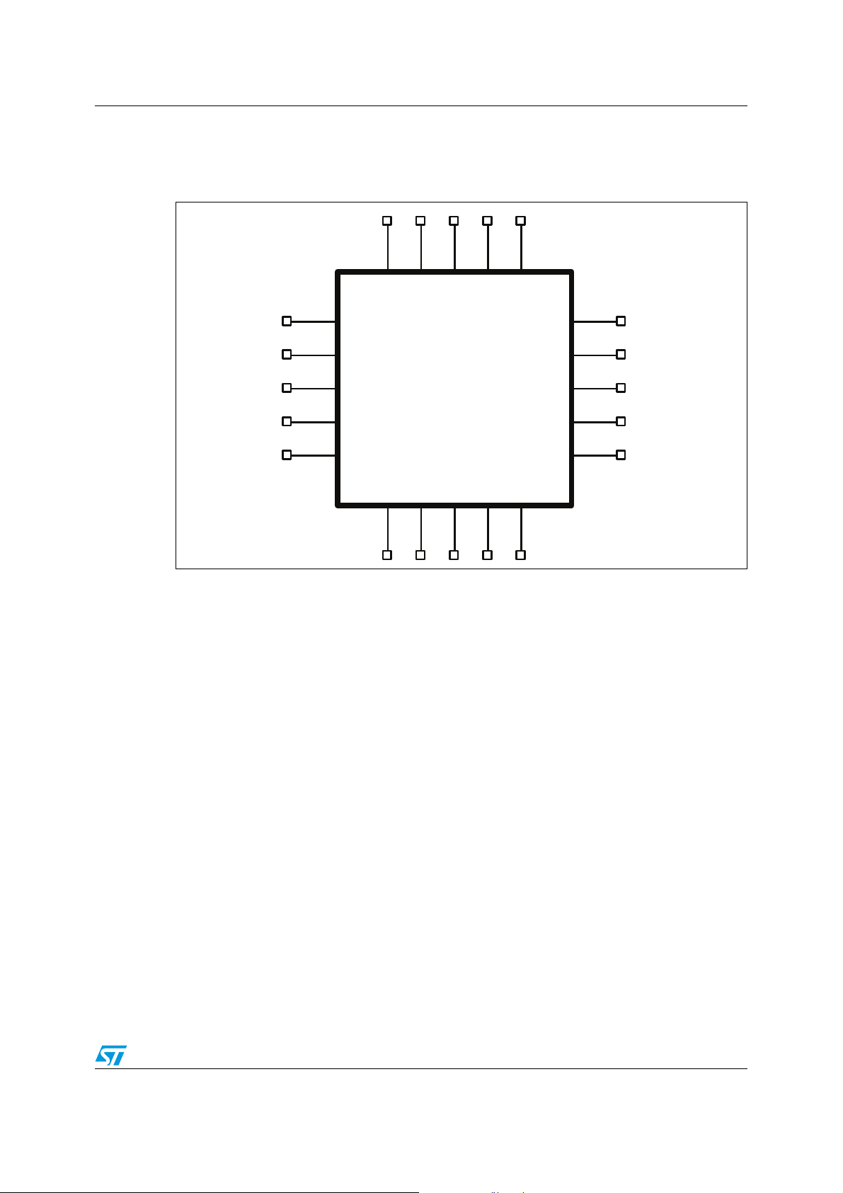
PM6613N Device pinout
2 Device pinout
Figure 2. PM6613N pinout
18
17
16
IOUT
ACOK
ILIM
ALARM#
15
14
ACDIV
13
B2B
12
ACDRV
11
ACP
19
20
SCL
1
SDA
PH
2
HIGH
3
BTST
PM6613N
4
LOW
5
GND
DCIN6SRP7SRN8BATFET9ACN
10
AM10244v1
Doc ID 022741 Rev 1 3/8

Package mechanical data PM6613N
3 Package mechanical data
In order to meet environmental requirements, ST offers these devices in different grades of
ECOPACK
specifications, grade definitions and product status are available at: www.st.com. ECOPACK
is an ST trademark.
®
packages, depending on their level of environmental compliance. ECOPACK
4/8 Doc ID 022741 Rev 1
PM6613N Package mechanical data
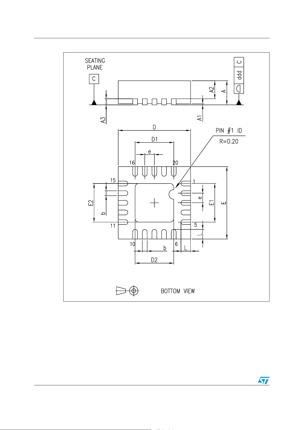
Table 2. QFN3x3 20L mechanical data
mm.
Dim.
Min. Typ. Max.
A 0.80 0.90 1.00
A1 0.02 0.05
A2 0.65 1.00
A3 0.20
b 0.15 0.20 0.25
D 2.85 3.00 3.15
D1 1.60
D2 1.50 1.60 1.70
E 2.85 3.00 3.15
E1 1.60
E2 1.50 1.60 1.70
e 0.35 0.40 0.45
L 0.30 0.40 0.50
ddd 0.07
Doc ID 022741 Rev 1 5/8
Package mechanical data PM6613N
Figure 3. QFN3x3 20L mechanical data drawing
6/8 Doc ID 022741 Rev 1
?2%6?!

PM6613N Revision history
4 Revision history
Table 3. Document revision history
Date Revision Changes
09-Feb-2012 1 Initial release.
Doc ID 022741 Rev 1 7/8

PM6613N
Please Read Carefully:
Information in this document is provided solely in connection with ST products. STMicroelectronics NV and its subsidiaries (“ST”) reserve the
right to make changes, corrections, modifications or improvements, to this document, and the products and services described herein at any
time, without notice.
All ST products are sold pursuant to ST’s terms and conditions of sale.
Purchasers are solely responsible for the choice, selection and use of the ST products and services described herein, and ST assumes no
liability whatsoever relating to the choice, selection or use of the ST products and services described herein.
No license, express or implied, by estoppel or otherwise, to any intellectual property rights is granted under this document. If any part of this
document refers to any third party products or services it shall not be deemed a license grant by ST for the use of such third party products
or services, or any intellectual property contained therein or considered as a warranty covering the use in any manner whatsoever of such
third party products or services or any intellectual property contained therein.
UNLESS OTHERWISE SET FORTH IN ST’S TERMS AND CONDITIONS OF SALE ST DISCLAIMS ANY EXPRESS OR IMPLIED
WARRANTY WITH RESPECT TO THE USE AND/OR SALE OF ST PRODUCTS INCLUDING WITHOUT LIMITATION IMPLIED
WARRANTIES OF MERCHANTABILITY, FITNESS FOR A PARTICULAR PURPOSE (AND THEIR EQUIVALENTS UNDER THE LAWS
OF ANY JURISDICTION), OR INFRINGEMENT OF ANY PATENT, COPYRIGHT OR OTHER INTELLECTUAL PROPERTY RIGHT.
UNLESS EXPRESSLY APPROVED IN WRITING BY TWO AUTHORIZED ST REPRESENTATIVES, ST PRODUCTS ARE NOT
RECOMMENDED, AUTHORIZED OR WARRANTED FOR USE IN MILITARY, AIR CRAFT, SPACE, LIFE SAVING, OR LIFE SUSTAINING
APPLICATIONS, NOR IN PRODUCTS OR SYSTEMS WHERE FAILURE OR MALFUNCTION MAY RESULT IN PERSONAL INJURY,
DEATH, OR SEVERE PROPERTY OR ENVIRONMENTAL DAMAGE. ST PRODUCTS WHICH ARE NOT SPECIFIED AS "AUTOMOTIVE
GRADE" MAY ONLY BE USED IN AUTOMOTIVE APPLICATIONS AT USER’S OWN RISK.
Resale of ST products with provisions different from the statements and/or technical features set forth in this document shall immediately void
any warranty granted by ST for the ST product or service described herein and shall not create or extend in any manner whatsoever, any
liability of ST.
ST and the ST logo are trademarks or registered trademarks of ST in various countries.
Information in this document supersedes and replaces all information previously supplied.
The ST logo is a registered trademark of STMicroelectronics. All other names are the property of their respective owners.
© 2012 STMicroelectronics - All rights reserved
STMicroelectronics group of companies
Australia - Belgium - Brazil - Canada - China - Czech Republic - Finland - France - Germany - Hong Kong - India - Israel - Italy - Japan -
Malaysia - Malta - Morocco - Philippines - Singapore - Spain - Sweden - Switzerland - United Kingdom - United States of America
www.st.com
8/8 Doc ID 022741 Rev 1
 Loading...