

2 to 4-cell Li-ion, Li-FePO4 battery charger with SMBus
QFN 3x3x1.0 16L
interface, N-channel RBFET and BATFET MOSFET selectors
Features
■ Buck converter
– Synchronous buck converter with N-
channel high-side, low-side Power
MOSFET integrated drivers
– 350 kHz or 700 kHz switching frequency,
selectable with SMBus
– AC adapter input voltage range 9 V - 24 V
– 5 V bias input voltage supply
– Battery charge voltage range 2.5 V - 18 V
– ±0.5% charge voltage accuracy
– 0.1% cell charge voltage resolution
– ±3% charge current accuracy
– Overvoltage, overcurrent protection
– Battery, inductor, Power MOSFET short-
circuit protection
– Internal loop compensation network
– Integrated soft-start
■ Selector
– N-channel BATFET MOSFET driver
– N-channel RBFET MOSFET driver
■ System
– 1 mA quiescent supply current
– 17 µA - 35 µA sleep mode current (BATFET
charge pump OFF - ON)
– Thermal shutdown
Application
PM6610
Data brief
MOSFET drivers. The possibility to set the
switching frequency with SMBus by choosing one
of the two preset values of 350 kHz or 700 kHz
assures the best trade-off between power
conversion efficiency and application component
cost and PCB size.
Integrated loop compensation network and softstart allow the reduction of the number of external
components.
The PM6610 integrates 2 charge pumps to drive
N-channel BATFET and RBFET MOSFETs.
The SMBus communication interface is used to
set the battery charge current and voltage.
The PM6610 charges 2 to 4-series Li-Ion or
LiFePO
available on a 16-pin, 3x3 mm, QFN package.
cells, for mobile PC applications. It is
4
■ Mobile PC:
– UMPC/MID and tablets
– Netbook and notebook computers
Table 1. Device summary
Order code Package Packing
PM6610 QFN 3x3x1.0 16L Tape and reel
Description
The PM6610 is a high efficiency battery charger
with SMBus communication interface. It includes
a synchronous switching DC-DC converter with
N-channel high-side and low-side Power
February 2012 Doc ID 022763 Rev 1 1/8
For further information contact your local STMicroelectronics sales office.
www.st.com
8
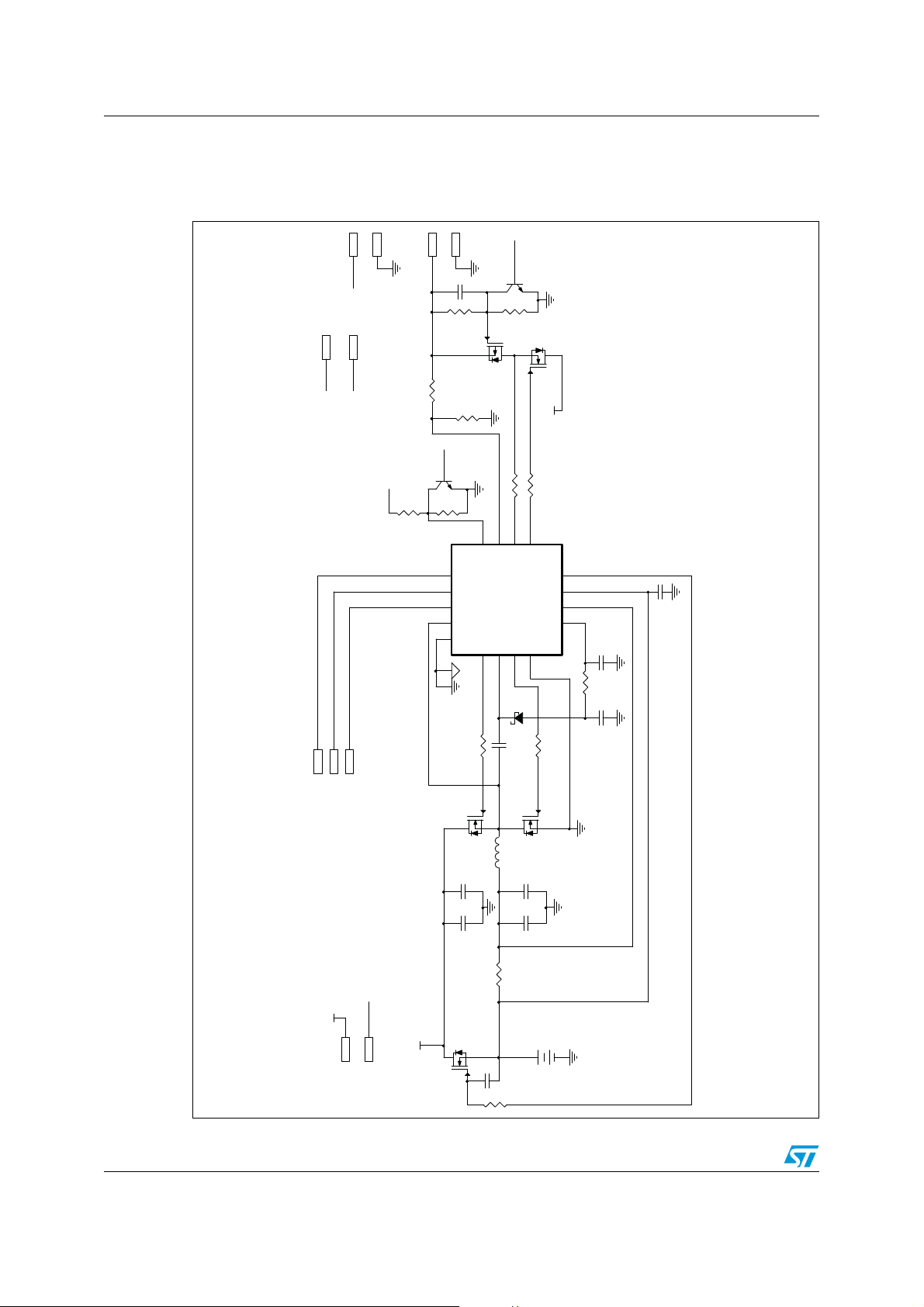
Typical application circuit PM6610
ILIM
GND
+5V
+5V
BYP
BYP
ILIM
ADP
GND
ACFET
ADP
R1 C1
R2
QBYP
BYP
RBFET
SYS
BATT
SYS
BATT
ACDIV
CSRN
SCL
SDA
ACOK
SCL
ACOK
SDA
SRN
SRP
ILIM
RAC
RB2B
RADL
RADU
QILIM
RILL
RILU
+5V
U1
PM6610
HIGH1BTST2LOW3GND
4
DCIN
5
SRP
6
SRN
7
BATFET
8
ACDR V
9
B2B
10
ACDIV
11
ILIM
12
ACOK
13
SCL
14
SDA
15
PH
16
THP
17
RB
SYS
BATFET
HS
LS
DCIN
L1
RHS
CDC
D1
RDC
CBT
COUT2
COUT1
RSB
BT1
BATTERY
C9
CIN2
CIN1
SYS
BATT
SYS
CBT1
+5V
BTSTPHASE
AM10263v1
1 Typical application circuit
Figure 1. Typical application circuit
2/8 Doc ID 022763 Rev 1
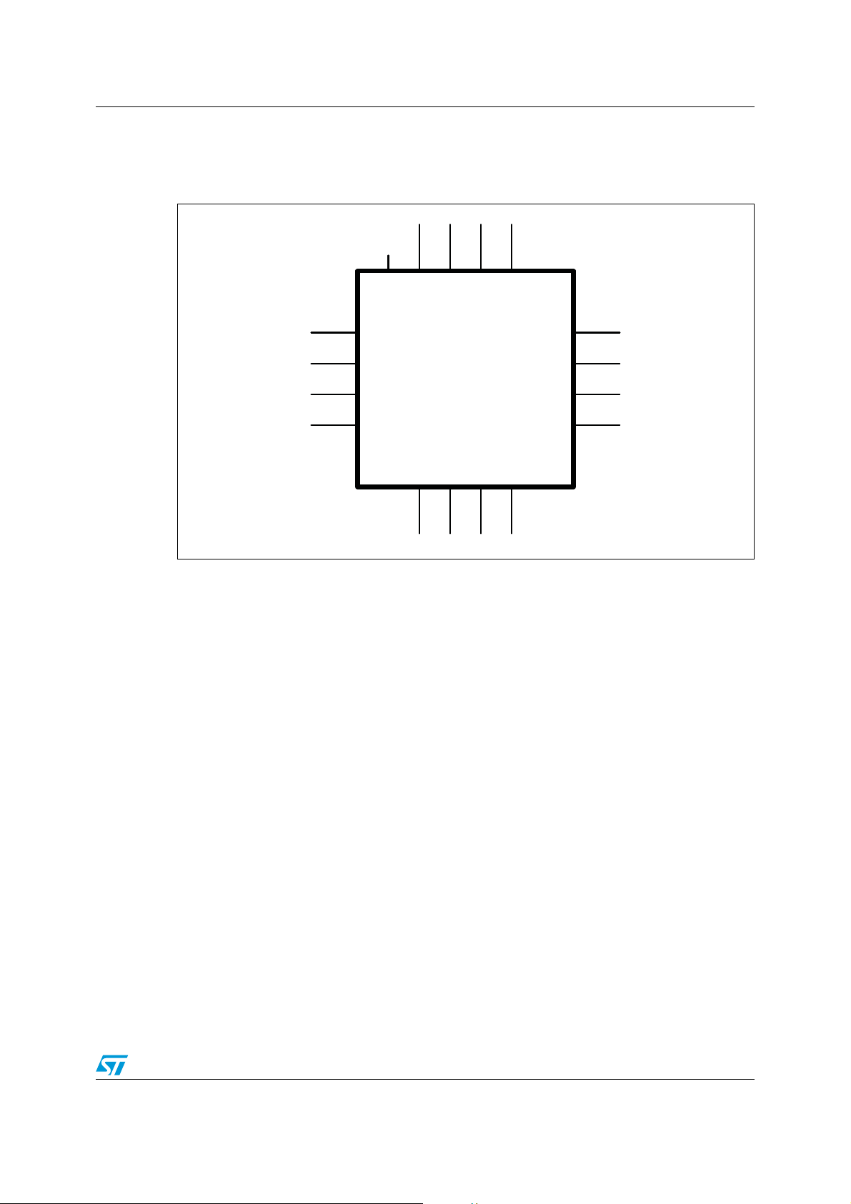
PM6610 Device pinout
PM6610
HIGH
1
BTST
2
LOW
3
GND
4
DCIN5SRP6SRN
7
BATF ET
8
ACDRV
9
B2B
10
ACDIV
11
ILIM
12
ACOK
13
SCL
14
SDA
15
PH
16
THP
17
AM10264v1
2 Device pinout
Figure 2. PM6610 pinout
Doc ID 022763 Rev 1 3/8
 Loading...