


6-row 32 mA LED driver with boost regulator
Features
■ Boost section
– 4.7 V to 28 V input voltage range
– Internal power MOSFET
– Internal +5 V LDO for device supply
– Up to 36 V output voltage
– Constant frequency peak current-mode
control
– 200 kHz to 1 MHz adjustable switching
frequency
– External synchronization for multi-device
application
– Pulse-skip power saving mode at light load
– Programmable soft-start
– Programmable OVP protection
– Stable with ceramic output capacitors
– Thermal shutdown
■ Backlight driver section
– Six rows with 32 mA maximum current
capability (adjustable)
– Up to 10 WLEDs per row
– Unused rows detection
– 500 ns minimum dimming time (1%
minimum dimming duty-cycle at 20 kHz)
– ± 2.1% current accuracy
– ± 2% current matching between rows
– LED failure (open and short circuit)
detection
PM6600
for LCD panel backlight
VFQFPN-24 4 mm x 4 mm
Description
The PM6600 consists of a high efficiency
monolithic boost converter and six controlled
current generators (ROWs), specifically designed
to supply LEDs arrays used in the backlight of
LCD panels. The device can manage a nominal
output voltage up to 36 V (i.e. 10 White-LEDs per
ROW). The generators can be externally
programmed to sink up to 32 mA and they can be
dimmed via a PWM signal (1% dimming dutycycle at 20 kHz can be managed). The device
allows to detect and manage the open and
shorted LED faults and to let unused ROWs
floating. Basic protections (output over-voltage,
internal MOSFET over-current and thermal
shutdown) are provided.
Applications
■ Notebook monitors backlight
■ UMPC backlight
Table 1. Device summary
February 2010 Doc ID 14248 Rev 7 1/60
Order codes Package Packaging
PM6600
PM6600TR Tape and reel
VFQFPN-24 4 mm x 4 mm
(exposed pad)
Tu b e
www.st.com
60

Contents PM6600
Contents
1 Typical application circuit . . . . . . . . . . . . . . . . . . . . . . . . . . . . . . . . . . . . 7
2 Pin settings . . . . . . . . . . . . . . . . . . . . . . . . . . . . . . . . . . . . . . . . . . . . . . . . 8
2.1 Connections . . . . . . . . . . . . . . . . . . . . . . . . . . . . . . . . . . . . . . . . . . . . . . . . 8
2.2 Pin description . . . . . . . . . . . . . . . . . . . . . . . . . . . . . . . . . . . . . . . . . . . . . . 8
3 Electrical data . . . . . . . . . . . . . . . . . . . . . . . . . . . . . . . . . . . . . . . . . . . . . 10
3.1 Maximum rating . . . . . . . . . . . . . . . . . . . . . . . . . . . . . . . . . . . . . . . . . . . . 10
3.2 Thermal data . . . . . . . . . . . . . . . . . . . . . . . . . . . . . . . . . . . . . . . . . . . . . . 10
3.3 Recommended operating conditions . . . . . . . . . . . . . . . . . . . . . . . . . . . . 11
4 Electrical characteristics . . . . . . . . . . . . . . . . . . . . . . . . . . . . . . . . . . . . 12
5 Typical operating characteristics . . . . . . . . . . . . . . . . . . . . . . . . . . . . . 15
6 Block diagram . . . . . . . . . . . . . . . . . . . . . . . . . . . . . . . . . . . . . . . . . . . . . 25
7 Operation description . . . . . . . . . . . . . . . . . . . . . . . . . . . . . . . . . . . . . . . 26
7.1 Boost section . . . . . . . . . . . . . . . . . . . . . . . . . . . . . . . . . . . . . . . . . . . . . . 26
7.1.1 Functional description . . . . . . . . . . . . . . . . . . . . . . . . . . . . . . . . . . . . . . 26
7.2 Overvoltage protection . . . . . . . . . . . . . . . . . . . . . . . . . . . . . . . . . . . . . . . 27
7.3 Switching frequency selection and synchronization . . . . . . . . . . . . . . . . . 28
7.4 System stability . . . . . . . . . . . . . . . . . . . . . . . . . . . . . . . . . . . . . . . . . . . . 30
7.4.1 Loop compensation . . . . . . . . . . . . . . . . . . . . . . . . . . . . . . . . . . . . . . . . 30
7.4.2 Slope compensation . . . . . . . . . . . . . . . . . . . . . . . . . . . . . . . . . . . . . . . 32
7.5 Soft-start . . . . . . . . . . . . . . . . . . . . . . . . . . . . . . . . . . . . . . . . . . . . . . . . . . 33
7.6 Boost current limit . . . . . . . . . . . . . . . . . . . . . . . . . . . . . . . . . . . . . . . . . . . 35
7.7 Enable function . . . . . . . . . . . . . . . . . . . . . . . . . . . . . . . . . . . . . . . . . . . . . 35
7.8 Thermal protection . . . . . . . . . . . . . . . . . . . . . . . . . . . . . . . . . . . . . . . . . . 36
8 Backlight driver section . . . . . . . . . . . . . . . . . . . . . . . . . . . . . . . . . . . . . 37
8.1 Current generators . . . . . . . . . . . . . . . . . . . . . . . . . . . . . . . . . . . . . . . . . . 37
8.2 PWM dimming . . . . . . . . . . . . . . . . . . . . . . . . . . . . . . . . . . . . . . . . . . . . . 38
2/60 Doc ID 14248 Rev 7

PM6600 Contents
9 Fault management . . . . . . . . . . . . . . . . . . . . . . . . . . . . . . . . . . . . . . . . . . 39
9.1 FAULT pin . . . . . . . . . . . . . . . . . . . . . . . . . . . . . . . . . . . . . . . . . . . . . . . . . 39
9.2 MODE pin . . . . . . . . . . . . . . . . . . . . . . . . . . . . . . . . . . . . . . . . . . . . . . . . . 39
9.3 Open LED fault . . . . . . . . . . . . . . . . . . . . . . . . . . . . . . . . . . . . . . . . . . . . . 40
9.4 Shorted LED fault . . . . . . . . . . . . . . . . . . . . . . . . . . . . . . . . . . . . . . . . . . . 40
9.5 Intermittent connection . . . . . . . . . . . . . . . . . . . . . . . . . . . . . . . . . . . . . . . 40
10 Package mechanical data . . . . . . . . . . . . . . . . . . . . . . . . . . . . . . . . . . . . 42
Appendix A Layout guidelines. . . . . . . . . . . . . . . . . . . . . . . . . . . . . . . . . . . . . . . . 44
A.1 Basic points: . . . . . . . . . . . . . . . . . . . . . . . . . . . . . . . . . . . . . . . . . . . . . . . 44
A.1.1 GNDs planes - 1 device . . . . . . . . . . . . . . . . . . . . . . . . . . . . . . . . . . . . . 44
A.1.2 GNDs planes - 3 devices (RGB) . . . . . . . . . . . . . . . . . . . . . . . . . . . . . . . 44
A.2 Compensation network . . . . . . . . . . . . . . . . . . . . . . . . . . . . . . . . . . . . . . . 44
A.3 LX area – vout power area . . . . . . . . . . . . . . . . . . . . . . . . . . . . . . . . . . . . 45
A.4 Overvoltage divider . . . . . . . . . . . . . . . . . . . . . . . . . . . . . . . . . . . . . . . . . . 45
A.5 LDO5 – AVCC filter . . . . . . . . . . . . . . . . . . . . . . . . . . . . . . . . . . . . . . . . . . 45
A.6 ROWs current generators . . . . . . . . . . . . . . . . . . . . . . . . . . . . . . . . . . . . . 45
A.7 Top layer of the standard PM6600 demonstration board. . . . . . . . . . . . . . 46
Appendix B Application note. . . . . . . . . . . . . . . . . . . . . . . . . . . . . . . . . . . . . . . . . 48
B.1 Inductor selection . . . . . . . . . . . . . . . . . . . . . . . . . . . . . . . . . . . . . . . . . . . 48
B.2 Capacitors selection . . . . . . . . . . . . . . . . . . . . . . . . . . . . . . . . . . . . . . . . . 48
B.3 Flywheel diode selection . . . . . . . . . . . . . . . . . . . . . . . . . . . . . . . . . . . . . . 48
B.4 Design example. . . . . . . . . . . . . . . . . . . . . . . . . . . . . . . . . . . . . . . . . . . . . 49
B.4.1 Switching frequency setting . . . . . . . . . . . . . . . . . . . . . . . . . . . . . . . . . . 49
B.4.2 Row current setting . . . . . . . . . . . . . . . . . . . . . . . . . . . . . . . . . . . . . . . . . 49
B.4.3 Inductor choice . . . . . . . . . . . . . . . . . . . . . . . . . . . . . . . . . . . . . . . . . . . . 49
B.4.4 Output capacitor choice . . . . . . . . . . . . . . . . . . . . . . . . . . . . . . . . . . . . . 51
B.4.5 Input capacitor choice. . . . . . . . . . . . . . . . . . . . . . . . . . . . . . . . . . . . . . . 52
B.4.6 Overvoltage protection divider setting. . . . . . . . . . . . . . . . . . . . . . . . . . . 52
B.4.7 Compensation network . . . . . . . . . . . . . . . . . . . . . . . . . . . . . . . . . . . . . . 53
B.4.8 Boost current limit . . . . . . . . . . . . . . . . . . . . . . . . . . . . . . . . . . . . . . . . . . 53
B.4.9 Soft-start . . . . . . . . . . . . . . . . . . . . . . . . . . . . . . . . . . . . . . . . . . . . . . . . . 54
Doc ID 14248 Rev 7 3/60

Contents PM6600
Appendix C Application suggestions . . . . . . . . . . . . . . . . . . . . . . . . . . . . . . . . . . 55
C.1 Full application schematic . . . . . . . . . . . . . . . . . . . . . . . . . . . . . . . . . . . . . 55
C.2 EN, DIM path in production line. . . . . . . . . . . . . . . . . . . . . . . . . . . . . . . . . 56
C.3 ROW pins protection . . . . . . . . . . . . . . . . . . . . . . . . . . . . . . . . . . . . . . . . . 57
C.4 Debug and measurements test points. . . . . . . . . . . . . . . . . . . . . . . . . . . . 57
C.5 Inductor choice . . . . . . . . . . . . . . . . . . . . . . . . . . . . . . . . . . . . . . . . . . . . . 58
11 Revision history . . . . . . . . . . . . . . . . . . . . . . . . . . . . . . . . . . . . . . . . . . . 59
4/60 Doc ID 14248 Rev 7

PM6600 List of figures
List of figures
Figure 1. Application circuit . . . . . . . . . . . . . . . . . . . . . . . . . . . . . . . . . . . . . . . . . . . . . . . . . . . . . . . . . 7
Figure 2. Pin connection (through top view) . . . . . . . . . . . . . . . . . . . . . . . . . . . . . . . . . . . . . . . . . . . . 8
Figure 3. Efficiency vs DIM duty cycle @ fDIM = 200 Hz. . . . . . . . . . . . . . . . . . . . . . . . . . . . . . . . . . 15
Figure 4. Efficiency vs DIM duty cycle @ fDIM = 500 Hz. . . . . . . . . . . . . . . . . . . . . . . . . . . . . . . . . . 15
Figure 5. Efficiency vs DIM duty cycle @ fDIM = 1 kHz. . . . . . . . . . . . . . . . . . . . . . . . . . . . . . . . . . . 15
Figure 6. Efficiency vs DIM duty cycle @ fDIM = 5 kHz. . . . . . . . . . . . . . . . . . . . . . . . . . . . . . . . . . . 15
Figure 7. Efficiency vs DIM duty cycle @ fDIM = 10 kHz. . . . . . . . . . . . . . . . . . . . . . . . . . . . . . . . . . 16
Figure 8. Efficiency vs DIM duty cycle @ fDIM = 20 kHz. . . . . . . . . . . . . . . . . . . . . . . . . . . . . . . . . . 16
Figure 9. Efficiency vs DIM duty cycle @ Vin = 8 V . . . . . . . . . . . . . . . . . . . . . . . . . . . . . . . . . . . . . . 16
Figure 10. Efficiency vs DIM duty cycle @ Vin = 12 V . . . . . . . . . . . . . . . . . . . . . . . . . . . . . . . . . . . . . 16
Figure 11. Efficiency vs DIM duty cycle @ Vin = 18 V . . . . . . . . . . . . . . . . . . . . . . . . . . . . . . . . . . . . . 16
Figure 12. Efficiency vs DIM duty cycle @ Vin = 24 V . . . . . . . . . . . . . . . . . . . . . . . . . . . . . . . . . . . . . 16
Figure 13. Efficiency vs Vin @ DIM duty cycles = 10% . . . . . . . . . . . . . . . . . . . . . . . . . . . . . . . . . . . . 17
Figure 14. Efficiency vs Vin @ DIM duty cycles = 50% . . . . . . . . . . . . . . . . . . . . . . . . . . . . . . . . . . . . 17
Figure 15. Efficiency vs Vin @ DIM duty cycles = 75% . . . . . . . . . . . . . . . . . . . . . . . . . . . . . . . . . . . . 17
Figure 16. Efficiency vs Vin @ DIM duty cycles = 100% . . . . . . . . . . . . . . . . . . . . . . . . . . . . . . . . . . . 17
Figure 17. Working waveforms @ fDIM = 100 Hz, D = 1% . . . . . . . . . . . . . . . . . . . . . . . . . . . . . . . . . 18
Figure 18. Working waveforms @ fDIM = 100 Hz, D = 10% . . . . . . . . . . . . . . . . . . . . . . . . . . . . . . . . 18
Figure 19. Working waveforms @ fDIM = 100 Hz, D = 50% . . . . . . . . . . . . . . . . . . . . . . . . . . . . . . . . 18
Figure 20. Working waveforms @ fDIM = 100 Hz, D = 80% . . . . . . . . . . . . . . . . . . . . . . . . . . . . . . . . 18
Figure 21. Working waveforms @ fDIM = 200 Hz, D = 1% . . . . . . . . . . . . . . . . . . . . . . . . . . . . . . . . . 19
Figure 22. Working waveforms @ fDIM = 200 Hz, D = 20% . . . . . . . . . . . . . . . . . . . . . . . . . . . . . . . . 19
Figure 23. Working waveforms @ fDIM = 200 Hz, D = 50% . . . . . . . . . . . . . . . . . . . . . . . . . . . . . . . . 19
Figure 24. Working waveforms @ fDIM = 200 Hz, D = 80% . . . . . . . . . . . . . . . . . . . . . . . . . . . . . . . . 19
Figure 25. Working waveforms @ fDIM = 500 Hz, D = 1% . . . . . . . . . . . . . . . . . . . . . . . . . . . . . . . . . 20
Figure 26. Working waveforms @ fDIM = 500 Hz, D = 50% . . . . . . . . . . . . . . . . . . . . . . . . . . . . . . . . 20
Figure 27. Working waveforms @ fDIM = 1 kHz, D = 1% . . . . . . . . . . . . . . . . . . . . . . . . . . . . . . . . . . 20
Figure 28. Working waveforms @ fDIM = 1 kHz, D = 50% . . . . . . . . . . . . . . . . . . . . . . . . . . . . . . . . . 20
Figure 29. Working waveforms @ fDIM = 10 kHz, D = 1% . . . . . . . . . . . . . . . . . . . . . . . . . . . . . . . . . 21
Figure 30. Working waveforms @ fDIM = 10 kHz, D = 50% . . . . . . . . . . . . . . . . . . . . . . . . . . . . . . . . 21
Figure 31. Working waveforms @ fDIM = 20 kHz, D = 1% . . . . . . . . . . . . . . . . . . . . . . . . . . . . . . . . . 21
Figure 32. Working waveforms @ fDIM = 20 Hz, D = 50% . . . . . . . . . . . . . . . . . . . . . . . . . . . . . . . . . 21
Figure 33. Output voltage ripple @ fDIM = 200 Hz, D = 1% . . . . . . . . . . . . . . . . . . . . . . . . . . . . . . . . 22
Figure 34. Output voltage ripple @ fDIM = 200 Hz, D = 20% . . . . . . . . . . . . . . . . . . . . . . . . . . . . . . . 22
Figure 35. Output voltage ripple @ fDIM = 200 Hz, D = 50% . . . . . . . . . . . . . . . . . . . . . . . . . . . . . . . 22
Figure 36. Output voltage ripple @ fDIM = 200 Hz, D = 80% . . . . . . . . . . . . . . . . . . . . . . . . . . . . . . . 22
Figure 37. Shorted LED protection @ fDIM = 200 Hz all WLEDs connected . . . . . . . . . . . . . . . . . . . 23
Figure 38. Shorted LED protection @ fDIM = 200 Hz 1 WLED shorted . . . . . . . . . . . . . . . . . . . . . . . 23
Figure 39. Shorted LED protection @ fDIM = 200 Hz 2 WLEDs shorted. . . . . . . . . . . . . . . . . . . . . . . 23
Figure 40. Shorted LED protection @ fDIM = 200 Hz 3 WLEDs shorted - ROW disabled . . . . . . . . . 23
Figure 41. Open ROW detection @ fDIM = 200 Hz . . . . . . . . . . . . . . . . . . . . . . . . . . . . . . . . . . . . . . . 24
Figure 42. Simplified block diagram . . . . . . . . . . . . . . . . . . . . . . . . . . . . . . . . . . . . . . . . . . . . . . . . . . . 25
Figure 43. AVCC filtering . . . . . . . . . . . . . . . . . . . . . . . . . . . . . . . . . . . . . . . . . . . . . . . . . . . . . . . . . . . 26
Figure 44. OVP threshold setting . . . . . . . . . . . . . . . . . . . . . . . . . . . . . . . . . . . . . . . . . . . . . . . . . . . . . 28
Figure 45. Multiple device synchronization . . . . . . . . . . . . . . . . . . . . . . . . . . . . . . . . . . . . . . . . . . . . . 28
Figure 46. External sync waveforms . . . . . . . . . . . . . . . . . . . . . . . . . . . . . . . . . . . . . . . . . . . . . . . . . . 29
Figure 47. Poor phase margin (a) and properly damped (b) load transient responses . . . . . . . . . . . . 31
Figure 48. Load transient response measurement set-up . . . . . . . . . . . . . . . . . . . . . . . . . . . . . . . . . . 32
Doc ID 14248 Rev 7 5/60

List of figures PM6600
Figure 49. Main loop and current loop diagram . . . . . . . . . . . . . . . . . . . . . . . . . . . . . . . . . . . . . . . . . . 32
Figure 50. Effect of slope compensation on small inductor current perturbation (D > 0.5) . . . . . . . . . 33
Figure 51. Soft-start sequence waveforms in case of floating ROWs . . . . . . . . . . . . . . . . . . . . . . . . . 34
Figure 52. fDIM enabling schematic . . . . . . . . . . . . . . . . . . . . . . . . . . . . . . . . . . . . . . . . . . . . . . . . . . 36
Figure 53. VFQFPN-24 mechanical data . . . . . . . . . . . . . . . . . . . . . . . . . . . . . . . . . . . . . . . . . . . . . . . 43
Figure 54. Top layer critical signals components assembly and layout . . . . . . . . . . . . . . . . . . . . . . . . 46
Figure 55. Top side . . . . . . . . . . . . . . . . . . . . . . . . . . . . . . . . . . . . . . . . . . . . . . . . . . . . . . . . . . . . . . . 47
Figure 56. Bottom side. . . . . . . . . . . . . . . . . . . . . . . . . . . . . . . . . . . . . . . . . . . . . . . . . . . . . . . . . . . . . 47
Figure 57. Inductor current in DCM operation . . . . . . . . . . . . . . . . . . . . . . . . . . . . . . . . . . . . . . . . . . . 50
Figure 58. Full application schematic. . . . . . . . . . . . . . . . . . . . . . . . . . . . . . . . . . . . . . . . . . . . . . . . . . 55
Figure 59. EN pin filter . . . . . . . . . . . . . . . . . . . . . . . . . . . . . . . . . . . . . . . . . . . . . . . . . . . . . . . . . . . . . 56
Figure 60. DIM pin filter . . . . . . . . . . . . . . . . . . . . . . . . . . . . . . . . . . . . . . . . . . . . . . . . . . . . . . . . . . . . 56
Figure 61. ROW pins protection. . . . . . . . . . . . . . . . . . . . . . . . . . . . . . . . . . . . . . . . . . . . . . . . . . . . . . 57
6/60 Doc ID 14248 Rev 7

PM6600 Typical application circuit
1 Typical application circuit
Figure 1. Application circuit
VBOOST
Cout
Rslope
C13
R1
D
C10
R2
9
18
16
17
25
LX
19
L
Cin
VIN+
OVSEL
VIN
8
SYNC
23
AVCC
6
AVCC
Cavcc
SLOPE
Rf ilt
FAULT
Cldo5
PGND
ROW111ROW212ROW313ROW414ROW515ROW6
PM6600
LDO5
7
DIM20EN21FAULT
22
EN
5
AVCC
DIM
SGND
THP D
COMP1MOD E
SW3
10
BILIM
3
RILIM
2
FSW
4
SS
24
Css
Rcomp
MOD E
Rbilim
Rrilim
SW2
FSW
AVCC
Rfsw
Ccomp
VIN-
Doc ID 14248 Rev 7 7/60
Pin settings PM6600
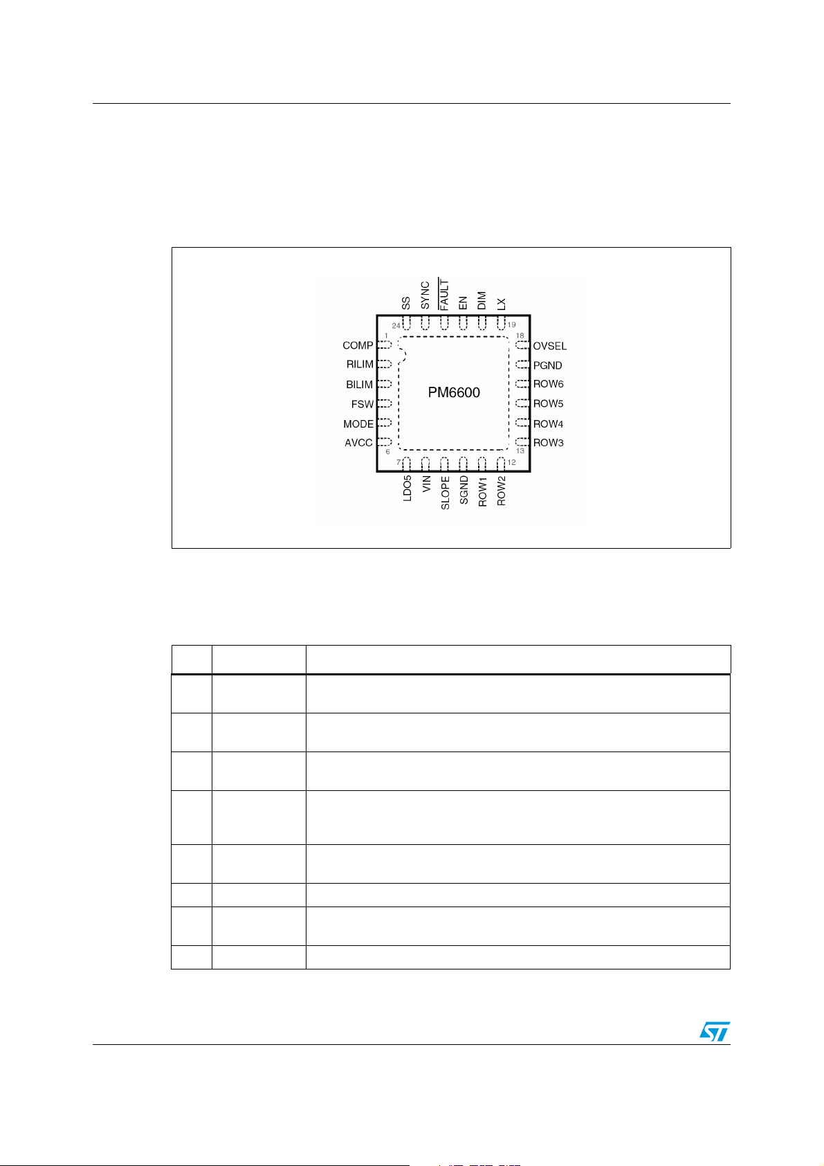
2 Pin settings
2.1 Connections
Figure 2. Pin connection (through top view)
2.2 Pin description
Table 2. Pin functions
N° Pin Function
1COMP
2 RILIM
3 BILIM
4FSW
5MODE
6 AVCC +5 V analog supply. Connect to LDO5 through a simple RC filter.
7LDO5
8 VIN Input voltage. Connect to the main supply rail.
Error amplifier output. A simple RC series between this pin and ground is
needed to compensate the loop of the boost regulator.
Output generators current limit setting. The output current of the ROWs can
be programmed connecting a resistor to SGND.
Boost converter current limit setting. The internal MOSFET current limit can
be programmed connecting a resistor to SGND.
Switching frequency selection and external sync input. A resistor to SGND
is used to set the desired switching frequency. The pin can also be used as
external synchronization input. See Section 7.3 on page 28 for details.
Current generators fault management selector. It allows to detect and
manage LEDs failures. See Section 9.2 on page 39 for details.
Internal +5 V LDO output and power section supply. Bypass to SGND with a
1 µF ceramic capacitor.
8/60 Doc ID 14248 Rev 7

PM6600 Pin settings
Table 2. Pin functions (continued)
N° Pin Function
Slope compensation setting. A resistor between the output of the boost
9SLOPE
converter and this pin is needed to avoid sub-harmonic instability.
Refer to section 1.4 for details.
10 SGND
Signal ground. Supply return for the analog circuitry and the current
generators.
11 ROW1 Row driver output #1.
12 ROW2 Row driver output #2.
13 ROW3 Row driver output #3.
14 ROW4 Row driver output #4.
15 ROW5 Row driver output #5.
16 ROW6 Row driver output #6.
17 PGND Power ground. Source of the internal power-MOSFET.
18 OVSEL
Over-voltage selection. Used to set the desired OV threshold by an external
divider. See Section 7.2 on page 27 for details.
19 LX Switching node. Drain of the internal power-MOSFET.
20 DIM
21 EN
22 FAULT
Dimming input. Used to externally set the brightness of the LEDs by using a
PWM signal.
Enable input. When low, the device is turned off. If tied high or left floating,
the device is turned on and a soft-start sequence takes place.
Fault signal output. Open drain output. The pin goes low when a fault
condition is detected (see Section 9.1 on page 39 for details).
23 SYNC Synchronization output. Used as external synchronization output.
24 SS
Soft-start. Connect a capacitor to SGND to set the desired soft-start
duration.
Doc ID 14248 Rev 7 9/60

Electrical data PM6600
3 Electrical data
3.1 Maximum rating
Table 3. Absolute maximum ratings
(1)
Symbol Parameter Value Unit
V
AVC C
V
LDO5
AVCC to SGND -0.3 to 6
LDO5 to SGND -0.3 to 6
PGND to SGND -0.3 to 0.3
V
IN
V
LX
VIN to PGND -0.3 to 40
LX to SGND -0.3 to 40
LX to PGND -0.3 to 40
RILIM, BILIM, SYNC, OVSEL, SS to SGND
V
AVC C
-0.3 to
+ 0.3
EN, DIM, FSW, MODE, FAULT to SGND -0.3 to 6
ROWx to PGND/ SGND -0.3 to 40
V
- 0.3 to
SLOPE to VIN
IN
V
+ 6
IN
SLOPE to SGND -0.3 to 40
Maximum LX RMS current 2.0 A
P
TOT
Power dissipation @ = 25 °C 2.3 W
Maximum withstanding voltage range test condition:
CDF-AEC-Q100-002- “human body model”
± 2000 V
acceptance criteria: “normal performance”
V
1. Stresses beyond those listed under “absolute maximum ratings” may cause permanent damage to the
device. Exposure to absolute maximum rated conditions for extended periods may affect device reliability.
3.2 Thermal data
Table 4. Thermal data
Symbol Parameter Value Unit
R
thJA
T
STG
T
T
10/60 Doc ID 14248 Rev 7
Thermal resistance junction to ambient 42 °C/W
Storage temperature range -50 to 150 °C
Junction operating temperature range -40 to 125 °C
J
Operating ambient temperature range -40 to 85 °C
A

PM6600 Electrical data
3.3 Recommended operating conditions
Table 5. Recommended operating conditions
Values
Symbol Parameter
Min Typ Max
Supply section
Unit
V
Input voltage range 4.7 - 28 V
IN
Boost section
V
BST
f
SW
Output voltage range - 36 V
Adjustable switching
frequency
FSW sync input
duty-cycle
I
rowx
ROWs output maximum
current
FSW connected
to R
FSW
200 - 1000 kHz
-40%
-32mA
Doc ID 14248 Rev 7 11/60

Electrical characteristics PM6600
4 Electrical characteristics
VIN = 12 V; TA = 0 °C to 85 °C and MODE connected to AVCC unless specified
Table 6. Electrical characteristics
Symbol Parameter Test condition
Supply section
V
LDO5, VAVC C
I
IN,Q
I
IN,SHDN
V
UVLO,ON
V
UVLO,OFF
LDO output and IC supply voltage
Operating quiescent current
Operating current in shutdown EN low 20 30 μA
LDO5 under voltage lockout upper
threshold
LDO5 under voltage lockout lower
threshold
LDO linear regulator
EN High,
= 0 mA
I
LDO5
R
= 51 kΩ,
RILIM
= 220 kΩ,
R
BILIM
R
SLOPE
= 680 kΩ
DIM tied to SGND.
(1)
.
Val ues
Unit
Min Typ Max
4.6 5 5.5 V
1mA
4.6 4.75
3.8 4.0
V
IN
= 30 mA
= 4.3 V,
= 10 mA
> V
< V
= 28 V,
UVLO,ON
UVLO,OFF
25 40 60
Line regulation
LDO dropout voltage
LDO maximum output current limit
1. TA = TJ. All parameters at operating temperature extremes are guaranteed by design and statistical analysis
(not production tested)
6 V = V
I
LDO5
V
IN
I
LDO5
V
LDO5
V
LDO5
25
mV
80 120
mA
30
12/60 Doc ID 14248 Rev 7

PM6600 Electrical characteristics
Table 6. Electrical characteristics (continued)
Val ues
Symbol Parameter Test condition
Min Typ Max
Boost section
Unit
t
on,min
Power switch
K
B
OV protections
Minimum switching
on time
200 ns
Default switching frequency FSW connected to AVCC 570 660 750
Minimum FSW
Sync frequency
FSW sync
Input low level threshold
FSW sync
Input hysteresis
FSW sync
Min ON time
SYNC output
duty-cycle
SYNC output
high level
SYNC output
low level
LX current coefficient R
Internal MOSFET R
DSon
240
FSW connected to AVCC
(Internal oscillator selected)
V
= 10 µA
I
SYNC
= -10 µA 20
I
SYNC
= 300 kΩ 5.7e5 6.7e5 7.7e5 V
BILIM
AVC C
-20
210
60
270 ns
34 40 %
280 500 mΩ
kHz
mV
mV
V
TH,OVP
V
TH,FRD
ΔV
OVP,FRD
Overvoltage protection reference
(OVSEL) threshold
Floating ROWs detection
(OVSEL) threshold
Voltage gap between the OVP
and FRD thresholds
1.190 1.235 1.280 V
1.100 1.145 1.190 V
90 mV
Doc ID 14248 Rev 7 13/60

Electrical characteristics PM6600
Table 6. Electrical characteristics (continued)
Val ues
Symbol Parameter Test condition
Min Typ Max
Soft-start and power management
EN, turn-on level threshold 1.6
Unit
EN, turn-off level threshold 0.8
DIM, high level threshold 1.3
DIM, low level threshold 0.8
EN, pull-up current 2.5
SS, charge current 4 5 6
SS, end-of-startup threshold 2 2.4 2.8
SS, reduced switching frequency
Release threshold
Current generators section
T
DIM-ON,min
K
R
ΔI
ROWx
V
IFB
V
TH,FAULT
V
FAU LT,L OW
Minimum dimming on-time R
ROWs current coefficient
accuracy
ROWs current mismatch
Feedback regulation voltage No LEDs mismatch 400 mV
Shorted LED fault detection
threshold
FAULT pin low-level voltage I
Thermal shutdown
(1)
0.8
= 51 kΩ 500 ns
RILIM
R
= 51 kΩ 998 ±21 V
RILIM
R
= 51 kΩ ±2 %
RILIM
8.2 V
FAULT,SINK
= 4 mA 350 mV
V
μA
V
T
SHDN
Thermal shutdown
Turn-off temperature
150 °C
Note: The current mismatch is the maximum current difference among the ROWs of one device.
14/60 Doc ID 14248 Rev 7

PM6600 Typical operating characteristics
5 Typical operating characteristics
All the measures are done with a standard PM6600EVAL demonstration board and a
standard WLED6021NB tamboured, with the components listed in the EVAL_KIT document.
The measures are done with this working conditions, unless specified:
● Vin = 12 V
● Vout = 6 rows x 10 WLEDs = 34 V (typ)
● Iout = 20 mA each row
● fsw = 660 kHz (nominal switching frequency, with FSW. AVCC)
● Vrow1 to Vrow6 = {0.697, 0.75, 0.818, 0.696, 0.822, 0.363} V
Figure 3. Efficiency vs
100
90
80
70
60
50
40
Effici ency [% ]
30
20
10
0
DIM duty cycle @ f
0 20406080100
DIM duty cycle [%]
= 200 Hz
DIM
Vin = 6V
Vin = 12V
Vin = 18V
Vin = 24V
Figure 4. Efficiency vs
DIM duty cycle @ f
100
90
80
70
60
50
40
Effici ency [% ]
30
20
10
0
020406080100
DIM du ty cycle [%]
DIM
= 500 Hz
Vin = 6V
Vin = 12V
Vin = 18V
Vin = 24V
Figure 5. Efficiency vs
100
90
80
70
60
50
40
Effici ency [%]
30
20
10
0
DIM duty cycle @ f
0 2040 6080100
DIM du ty cycl e [%]
= 1 kHz
DIM
Vin = 6V
Vin = 12V
Vin = 18V
Vin = 24V
Figure 6. Efficiency vs
DIM duty cycle @ f
100
90
80
70
60
50
40
Effici ency [%]
30
20
10
0
0 20406080100
Doc ID 14248 Rev 7 15/60
DIM du ty cycle [%]
= 5 kHz
DIM
Vin = 6V
Vin = 12V
Vin = 18V
Vin = 24V

Typical operating characteristics PM6600
Figure 7. Efficiency vs
100
90
80
70
60
50
40
Effic iency [%]
30
20
10
0
0 20406080100
DIM duty cycle @ f
DIM duty cyc le [%]
= 10 kHz
DIM
Vin = 6V
Vin = 12V
Vin = 18V
Vin = 24V
Figure 9. Efficiency vs
100
90
80
70
60
50
40
Effici ency [% ]
30
20
10
0
DIM duty cycle @ Vin = 8 V
fDIM = 200Hz
fDIM = 500Hz
fDIM = 1k Hz
fDIM = 5k Hz
fDIM = 10kHz
fDIM = 20kHz
0 20406080100
DIM du ty cycle [%]
Figure 8. Efficiency vs
DIM duty cycle @ f
100
90
80
70
60
50
40
Efficien cy [%]
30
20
10
0
0 20 40 60 80 100
DIM du ty cycle [%]
DIM
= 20 kHz
Vin = 6V
Vin = 12V
Vin = 18V
Vin = 24V
Figure 10. Efficiency vs
DIM duty cycle @ Vin = 12 V
100
90
80
70
60
50
40
Effici ency [% ]
30
20
10
0
020406080100
DIM duty cycle [%]
fDIM = 200 Hz
fDIM = 500 Hz
fDIM = 1k Hz
fDIM = 5k Hz
fDIM = 10k Hz
fDIM = 20k Hz
Figure 11. Efficiency vs
100
90
80
70
60
50
40
Effici ency [%]
30
20
10
0
16/60 Doc ID 14248 Rev 7
DIM duty cycle @ Vin = 18 V
fDIM = 200Hz
fDIM = 500Hz
fDIM = 1k Hz
fDIM = 5k Hz
fDIM = 10k Hz
fDIM = 20k Hz
020406080100
DIM d uty cycl e [%]
Figure 12. Efficiency vs
DIM duty cycle @ Vin = 24 V
100
90
80
70
60
50
40
Effici ency [%]
30
20
10
0
0 20406080100
DIM duty cycle [%]
fDIM = 200 Hz
fDIM = 500 Hz
fDIM = 1k Hz
fDIM = 5k Hz
fDIM = 10k Hz
fDIM = 20k Hz

PM6600 Typical operating characteristics
Figure 13. Efficiency
100
90
80
70
60
50
40
Effici ency [%]
30
20
10
0
vs Vin @ DIM duty cycles = 10%
fDIM = 200Hz
fDIM = 500Hz
fDIM = 1k Hz
fDIM = 5k Hz
fDIM = 10k Hz
fDIM = 20k Hz
6121824
Vin [V]
Figure 14. Efficiency
vs Vin @ DIM duty cycles = 50%
100
90
80
70
60
50
40
Effici ency [%]
30
20
10
0
6 121824
Vin [V]
fDIM = 200Hz
fDIM = 500Hz
fDIM = 1k Hz
fDIM = 5k Hz
fDIM = 10k Hz
fDIM = 20k Hz
Figure 15. Efficiency
96
94
92
90
88
Efficien cy [%]
86
84
82
6121824
vs Vin @ DIM duty cycles = 75%
fDIM = 200Hz
fDIM = 500Hz
fDIM = 1k Hz
fDIM = 5k Hz
fDIM = 10k Hz
fDIM = 20k Hz
Vin [V]
Figure 16. Efficiency
vs Vin @ DIM duty cycles = 100%
95
94
93
92
91
90
Efficiency [%]
89
88
87
6 121824
Vin [V]
fDIM = 200Hz
fDIM = 500Hz
fDIM = 1k Hz
fDIM = 5k Hz
fDIM = 10k Hz
fDIM = 20k Hz
Doc ID 14248 Rev 7 17/60

Typical operating characteristics PM6600
Figure 17. Working waveforms @
f
= 100 Hz, D = 1%
DIM
Figure 18. Working waveforms @
f
= 100 Hz, D = 10%
DIM
Figure 19. Working waveforms @
f
= 100 Hz, D = 50%
DIM
Figure 20. Working waveforms @
f
= 100 Hz, D = 80%
DIM
18/60 Doc ID 14248 Rev 7

PM6600 Typical operating characteristics
Figure 21. Working waveforms @
f
= 200 Hz, D = 1%
DIM
Figure 23. Working waveforms @
f
= 200 Hz, D = 50%
DIM
Figure 22. Working waveforms @
f
= 200 Hz, D = 20%
DIM
Figure 24. Working waveforms @
f
= 200 Hz, D = 80%
DIM
Doc ID 14248 Rev 7 19/60

Typical operating characteristics PM6600
Figure 25. Working waveforms @
f
= 500 Hz, D = 1%
DIM
Figure 27. Working waveforms @
f
= 1 kHz, D = 1%
DIM
Figure 26. Working waveforms @
f
= 500 Hz, D = 50%
DIM
Figure 28. Working waveforms @
f
= 1 kHz, D = 50%
DIM
20/60 Doc ID 14248 Rev 7

PM6600 Typical operating characteristics
Figure 29. Working waveforms @
f
= 10 kHz, D = 1%
DIM
Figure 31. Working waveforms @
f
= 20 kHz, D = 1%
DIM
Figure 30. Working waveforms @
f
= 10 kHz, D = 50%
DIM
Figure 32. Working waveforms @
f
= 20 Hz, D = 50%
DIM
Doc ID 14248 Rev 7 21/60

Typical operating characteristics PM6600
Figure 33. Output voltage ripple @
f
= 200 Hz, D = 1%
DIM
Figure 35. Output voltage ripple @
f
= 200 Hz, D = 50%
DIM
Figure 34. Output voltage ripple @
f
= 200 Hz, D = 20%
DIM
Figure 36. Output voltage ripple @
f
= 200 Hz, D = 80%
DIM
22/60 Doc ID 14248 Rev 7

PM6600 Typical operating characteristics
Figure 37. Shorted LED protection
@ f
= 200 Hz
DIM
all WLEDs connected
Figure 39. Shorted LED protection
@ f
= 200 Hz
DIM
2 WLEDs shorted
Figure 38. Shorted LED protection
@ f
= 200 Hz
DIM
1 WLED shorted
Figure 40. Shorted LED protection
@ f
= 200 Hz
DIM
3 WLEDs shorted - ROW disabled
Doc ID 14248 Rev 7 23/60

Typical operating characteristics PM6600
Figure 41. Open ROW detection @
f
= 200 Hz
DIM
24/60 Doc ID 14248 Rev 7

PM6600 Block diagram
_
CO
SYNC
U
G
6
O
SLO
CC
3
O
5
OVS
SG
O
g
O
6 Block diagram
Figure 42. Simplified block diagram
BILIM
FSW
AV
M
FA
MP
EN
DE
LT
VIN
+5V
LD
UVLO
Detector
UVLO
Current Limit
Soft Start
Prot_EN
Ext Sync
Detector
CONTROL
LOGIC
Thermal
PE
Current Sense
Ramp
Generator
+
+
÷2
OSC
Prot_EN
Boost_EN
UVLO
CTRL6
CTRL5
CTRL4
CTRL3
CTRL2
OVP
FRD
1.2V
+
m
_
Min Voltage
Selector
I to V
CTRL1
V
ROW1
ZCD
+
Boost
Control
_
Logic
0.4V
Boost_EN
FRD
OVP
VROW6
CTRL6
VROW5
CTRL5
VROW4
CTRL4
VROW3
CTRL3
VROW2
CTRL2
Generator 1
Current
LOGIC
Current
Generator 6
Current
Generator 5
Current
Generator 4
Current
Generator 3
Current
Generator 2
8.2V
I to V
+
_
_
+
+
VTH,FLT
1.143V
1.235V
LX
P
ND
EL
ROW
ROW
ROW4
ROW
R
W2
R
W1
RILIM
ND
Doc ID 14248 Rev 7 25/60

Operation description PM6600
7 Operation description
7.1 Boost section
7.1.1 Functional description
The PM6600 is a monolithic LEDs driver for the backlight of LCD panels and it consists of a
boost converter and six PWM-dimmable current generators.
The input voltage range is from 4.7 V up to 28 V.
The boost section is based on a constant switching frequency, Peak Current-Mode
architecture. The boost output voltage is controlled such that the lowest ROWs' voltage,
referred to SGND, is equal to an internal reference voltage (400 mV typ.).
In addition, the PM6600 has an internal LDO that supplies the internal circuitry of the device
and is capable to deliver up to 40 mA. The input of the LDO is the VIN pin. The LDO5 pin is
the LDO output and the supply for the power-MOSFET driver at the same time. The AVCC
pin is the supply for the analog circuitry and should be connected to the LDO output through
a simple RC filter, in order to improve the noise rejection.
Figure 43. AVCC filtering
VIN
Rfilt
4R7
Cavcc
100n
LDO5
AVCC
LDO
PM6600
SGND
Two loops are involved in regulating the current sunk by the generators.
The main loop is related to the boost regulator and uses a constant frequency peak currentmode architecture (see Figure 49), while an internal current loop regulates the same current
at each ROW according to the set value (RILIM pin).
A dedicated circuit automatically selects the lowest voltage drop among all the ROWs and
provides this voltage the main loop that, in turn, regulates the output voltage. In fact, once
the reference generator has been detected, the error amplifier compares its voltage drop to
the internal reference voltage and varies the COMP output. The voltage at the COMP pin
determines the inductor peak current at each switching cycle. The output voltage of the
boost regulator is thus determined by the total forward voltage of the LEDs strings:
Equation 1
OUT
N
ROWS
=
1i
m
LEDS
mV400)V(maxV
+=
j,F
Σ
=
1j
26/60 Doc ID 14248 Rev 7

PM6600 Operation description
++<<+
+⋅=
where the first term represents the highest total forward voltage drop over active ROWs and
the second is the voltage drop across the leading generator (400 mV typ.).
The device continues to monitor the voltage drop across all the rows and automatically
switches to the current generator having the lowest voltage drop.
7.2 Overvoltage protection
An adjustable over-voltage protection is available. It can be set feeding the OVSEL pin with a
partition of the output voltage. The voltage of the central tap of the divider is thus compared
to a fixed 1.235 V threshold. When the voltage on the OVSEL pin exceeds the OV threshold,
the FAULT pin is tied low (see
condition is latched and the PM6600 is restarted by toggling the EN pin or by performing a
power-on reset (the POR occurs when the LDO output falls below the lower UVLO threshold
and subsequently crosses the upper UVLO threshold during the rising phase of the input
voltage). Normally, the value of the high-side resistors of the divider is in the order of 100k
to reduce the output capacitor discharge when the boost converter is off (during the off
phase of the dimming cycle).
The OVSEL divider should be a compensated one, with the capacitors C10 (typically in the
100 pF-330 pF range) that improves noise rejection at the OVSEL pin (see
C13 (typically 22 pF) that avoids OVP fault detection when a row is open.
Section 9 on page 39) and the device is turned off; this
Ω
Figure 44) and
The following formulas permit to properly select the OVP threshold, according to the VOUT
value and considering the worst case (maximum VF_WLED):
Equation 2
maxOUTOUTOVPmaxOUT
)V5.4VVVV3V
Equation 3
V4.0VnV
V
OUTmax
V
OVP
is the maximum output voltage considering the LED spread.
is the over-voltage protection threshold
maxWLED_Fseries_WLEDmaxOUT
The formula to choose the proper values for the resistors of the OVP divider is:
Equation 4
R1R
2
⎝⎠
1.235 1–
VOVP
⎛⎞
----------------------- -
=
Equation 5
R
2
C
1.5 C⋅
13
------ -
⋅=
10
R
1
Doc ID 14248 Rev 7 27/60

Operation description PM6600
Figure 44. OVP threshold setting
VIN
PM6600
LX
SGND
R1
OVSEL
R2
VOUT
C13
COUT
C10
7.3 Switching frequency selection and synchronization
The switching frequency of the boost converter can be set in the 200 kHz-1 MHz range by
connecting the FSW pin to ground through a resistor. Calculation of the setting resistor is
made using equation 3 and should not exceed the 80 kΩ-400 kΩ range.
Equation 6
f
SW
=
R
FSW
In addition, when the FSW pin is tied to AVCC, the PM6600 uses a default 660 kHz fixed
switching frequency, allowing to save a resistor in minimum components-count applications.
5.2
Figure 45. Multiple device synchronization
SLAVE
Sync Out
SYNC
PM6600
SGND
RFSW
MASTER
AVCC
FSW SYNC
SYNC
FSW
PM6600
SGND
The FSW pin can also be used as a synchronization input, allowing the PM6600 to operate
both as master or slave device. If a clock signal with a 210 kHz minimum frequency is
applied to this pin, the device locks synchronized (300 mV threshold). An Internal time-out
allows synchronization as long as the external clock frequency is greater than 210 kHz.
Keeping the FSW pin voltage lower than 300 mV for more than 1/210 kHz
≈ 5 μs results in
the device turn off. Normal operation is resumed as soon as FSW rises above the
mentioned threshold and the soft-start sequence is repeated.
28/60 Doc ID 14248 Rev 7

PM6600 Operation description
The SYNC pin is a synchronization output and provides a 34% (typ.) duty-cycle clock when
the PM6600 is used as master or a replica of the FSW pin when used as slave. It is used to
connect multiple devices in a daisy-chain configuration or to synchronize other switching
converters running in the system with the PM6600 (master operation).
When an external synchronization clock is applied to the FSW pin, the internal oscillator is
over-driven: each switching cycle begins at the rising edge of clock, while the slope
compensation ramp starts at the falling edge of the same signal. Thus, the external
synchronization clock is required to have a 40% maximum duty-cycle when the boost
converter is working in continuous-conduction mode (CCM). The minimum pulse width
which allows the synchronizing pulses to be detected is 270 ns.
Figure 46. External sync waveforms
FSW pin voltage (ext. sync)
Slave SYNC pin voltage
Slave LX pin voltage
270ns minimum
300mV threshold
Doc ID 14248 Rev 7 29/60

Operation description PM6600
⋅
≤
7.4 System stability
The boost section of the PM6600 is a fixed frequency, peak current-mode converter. During
normal operation, a minimum voltage selection circuit compares all the voltage drops across
the active current generators and provides the minimum one to the error amplifier. The
output voltage of the error amplifier determines the inductor peak current in order to keep its
inverting input equal to the reference voltage (400 mV typ). The compensation network
consists of a simple RC series (R
The calculation of R
COMP
dynamic performance of the boost converter and is strictly related to the operating
conditions.
7.4.1 Loop compensation
The compensation network can be quickly calculated using equations 4 through 9. Once
both R
order to get the optimal dynamic performance from the application.
The first parameter to be fixed is the switching frequency. Normally, a high switching
frequency allows reducing the size of the inductor but increases the switching losses and
negatively affects the dynamic response of the converter. For most of applications, the fixed
value (660 kHz) represents a good trade-off between power dissipation and dynamic
response, allowing to save an external resistor at the same time. In low-profile applications,
the inductor value is often kept low to reduce the number of turns; an inductor value in the
4.7 µH-15 µH range is a good starting choice.
COMP
and C
COMP
and C
have been determined, a fine-tuning phase may be required in
- C
COMP
is fundamental to achieve optimal loop stability and
COMP
) between the COMP pin and ground.
COMP
Even if the loop bandwidth of the boost converter should be chosen as large as possible, it
should be set to 20% of the switching frequency, taking care not to exceed the CCM-mode
right half-plane zero (RHPZ).
Equation 7
f2.0f
SWU
Equation 8
min,IN
OUT
2
⎞
⎟
⎟
⎠
⋅π
⎞
⎛
V
OUT
⎟
⎜
⎟
⎜
I
OUT
⎠
⎝
L2
is the overall output current,
V
OUT
I
OUT
V
⎛
⎜
2.0
R =
⎜
⎝
⋅=
OUT
V
2
RM
2.0f
U
Where V
Note that, the lower the inductor value (or the lower the switching frequency) the higher the
bandwidth can be achieved. The output capacitor is directly involved in the loop of the boost
is the minimum input voltage, I
IN,min
⋅≤
M =
L2
⋅π
V
min,IN
V
OUT
converter and must be large enough to avoid excessive output voltage drop in case of a
sudden line transition from the maximum to the minimum input voltages (ΔV
should not
OUT
exceed 50-100 mV):
30/60 Doc ID 14248 Rev 7

PM6600 Operation description
Equation 9
OUT
⎛
⎜
⎜
Cf2
⋅⋅π
U
⎝
V
OUT
I
=Δ
Once the output capacitor has been chosen, the R
Equation 10
R
COMP
=
Where GM = 2.7 S and gEA = 375 µS.
The C
capacitor is determined to place the frequency of the compensation zero 5
COMP
times lower than the loop bandwidth:
Equation 11
C
COMP
=
Where fZ = fU / 5.
The close loop gain function (G
) is thus given by equation 10:
LOOP
Equation 12
1
−
COMP
U
EAM
1
⋅⋅π
Rf2
V
V
⎞
MIN_IN
⎟
⎟
MAX_IN
⎠
can be calculated as:
Cf2
⋅⋅π
MgG
⋅⋅
COMPZ
−
⎛
⎜
RgGG
⎜
⎝
+⋅⋅=
COMPEAMLOOP
sC
1
COMP
⎞
⎟
⋅
⎟
⎠
RM
s1
+
A simple technique to optimize different applications is to replace R
trimmer and adjust its value to properly damp the output transient response. Insufficient
damping will result in excessive ringing at the output and poor phase margin. Figures 5a and
5b give an example of compensation adjustment for a typical application.
Figure 47. Poor phase margin (a) and properly damped (b) load transient responses
L
2
sRC1
COMP
RM
with a 20 kΩ
Doc ID 14248 Rev 7 31/60

Operation description PM6600
Figure 48. Load transient response measurement set-up
LDO5
BILIM
RILIM
SS
COMP
SGND
6.8μH
VIN= 6V
+5V
C
IN
7.4.2 Slope compensation
The constant frequency, peak current-mode topology has the advantage of very easy loop
compensation with output ceramic capacitors (reduced cost and size of the application) and
fast transient response. In addition, the intrinsic peak-current measurement simplifies the
current limit protection, avoiding undesired saturation of the inductor.
On the other side, this topology has a drawback: there is inherent open loop instability when
operating with a duty-ratio greater than 0.5. This phenomenon is known as “sub-harmonic
instability” and can be avoided by adding an external ramp to the one coming from the
sensed current. This compensating technique, based on the additional ramp, is called
“Slope Compensation”. In figure 11, where the switching duty-cycle is higher than 0.5, the
small perturbation ΔIL dies away in subsequent cycles thanks to the slope compensation
and the system reverts to a stable situation.
AVCC
DIM
LX
VIN
PM6600
FAULT
EN
VBST=30÷36V
4.7μF
MLCC
FSW
OVSEL
SLOPE
ROW1
ROW2
ROW3
ROW4
ROW5
ROW6
PGND
SYNC
MODE
Up to 10 WLEDs per row
R
=
L
500Hz
VBST
50mA
Figure 49. Main loop and current loop diagram
VIN
32/60 Doc ID 14248 Rev 7
COMP
PWM
g
m
LX
0.4V
Minimum voltage drop
selector
ROWx
SGND
RILIM

PM6600 Operation description
The SLOPE pin allows to properly set the amount of slope compensation connecting a
simple resistor R
between the SLOPE pin and the output. The compensation ramp
SLOPE
starts at 35% (typ.) of each switching period and its slope is given by the following equation:
Equation 13
⎞
VVV
−−
BEINOUT
⎟
⎟
⎠
Where K
⎛
KS
=
, VBE = 2 V (typ.) and SE is the slope ramp in [A/s].
SLOPE
⎜
SLOPEE
⎜
R
⎝
SLOPE
To avoid sub-harmonic instability, the compensating slope should be at least half the slope
of the inductor current during the off-phase for a duty-cycle greater than 50% (i.e. at the
lowest input voltage). The value of R
can be calculated according to equation 9.
SLOPE
Equation 14
)VVV(LK2
−−⋅⋅⋅
R
SLOPE
≤
)VV(
−
INOUT
BEINOUTSLOPE
Figure 50. Effect of slope compensation on small inductor current perturbation
(D > 0.5)
Inductor current (CCM)
0.35·T
SW
Programmed inductor peak current with
slope compensation (S
I
TRIP
E)
7.5 Soft-start
The soft-start function is required to perform a correct start-up of the system, controlling the
inrush current required to charge the output capacitor and to avoid output voltage overshoot.
The soft-start duration is set connecting an external capacitor between the SS pin and
ground. This capacitor is charged with a 5 μA constant current, forcing the voltage on the SS
pin to ramp up. When this voltage increases from zero to nearly 1.2 V, the current limit of the
power-MOSFET is proportionally released to its final value. In addition, during the initial part
of the Soft-Start, the switching frequency of the boost converter is reduced to half of the
ΔI
Inductor current
perturbation
L
T
SW
t
Doc ID 14248 Rev 7 33/60

Operation description PM6600
nominal value to permit to use inductors with lower saturation current value; the nominal
switching frequency is restored after the SS pin voltage has crossed 0.8 V. In this mode, the
current runaway is avoided.
Figure 51. Soft-start sequence waveforms in case of floating ROWs
OVP
Floating ROWs detection
Vth,FRD=
93% of OVP
Output voltage
AVCC
2.4V
1.2V
0.8V
SS pin voltage
Protections turn active
Nominal switching
frequency release
tss
100%
Current limit
EN pin voltage
t
During the soft-start phase it is also performed the floating ROWs detection. In presence of
one or more floating ROWs, the error amplifier is unbalanced and the output voltage
increases; when it reaches the floating ROW Detection (FRD) threshold (93% of the OVP
threshold), the floating ROWs are managed according to
39
). After the SS voltage reaches a 2.4 V threshold, the start-up finishes and all the
protections turn active. The soft-start duration can be calculated with the following formula:
Equation 15
Ta bl e 8 (see Section 9 on page
Where ISS = 5 µA.
Please refer to the application note section for the CSS value settings according to the
different working conditions.
34/60 Doc ID 14248 Rev 7
SS
C
SS
5.2t ≅
I
SS

PM6600 Operation description
7.6 Boost current limit
The design of the external components, especially the inductor and the flywheel diode, must
be optimized in terms of size relying on the programmable peak current limit. The PM6600
improves the reliability of the final application giving the way to limit the maximum current
flowing into the critical components. A simple resistor connected between the BILIM pin and
ground sets the desired value. The voltage at the BILIM pin is internally fixed to 1.2 V and
the current limit is proportional to the current flowing through the setting resistor, according
to the following equation:
Equation 16
K
I =
PEAK,BOOST
R
B
BILIM
where .
B
5
The maximum allowed current limit is 5 A, resulting in a minimum setting resistor
R
> 120 kΩ. The maximum guaranteed RMS current in the power switch is 2 Arms. The
BILIM
current limitation works by clamping the COMP pin voltage proportionally to R
inductor current is limited to the above threshold decreased by the slope compensation
contribution.
In a boost converter the r.m.s. current through the internal MOSFET depends on both the
input and output voltages, according to equations 15a (DCM) and 15b (CCM).
Equation 17 a
Equation 17 b
7.7 Enable function
%15V107.6K
±⋅=
. Peak
BILIM
DV
⋅
I
rms,MOS
⎛
D
=
⎜
II
OUTrms,MOS
⎜
()
−
D1
⎝
IN
=
SW
⎛
1
⎜
+
⎜
2
12
⎝
D
3
LF
⋅
V
OUT
SWOUT
2
⎞
⎟
()()
⎟
⋅⋅
LfI
⎠
⎞
3
⎟
−
D1D
⎟
⎠
The PM6600 is enabled by the EN pin. This pin is active high and, when forced to SGND,
the device is turned off. This pin is connected to a permanently active 2 μA current source;
when sudden device turn-on at power-up is required, this pin must be left floating or
connected to a delay capacitor. When turned off, the PM6600 quickly discharges the SoftStart capacitor and turns off the power-MOSFET, the current generators and the LDO. The
power consumption is thus reduced to 20 μA only.
The proper startup sequence is DIM ' VIN ' EN, or VIN ' DIM ' EN. If the dimming signal is
applied after the EN pin, the device will not perform the soft-start again, in fact it will start
switching with the maximum current limit in order to recover the output voltage.
In applications where the dimming signal is used to turn on and off the device, the EN pin
can be connected to the DIM pin as shown in
Doc ID 14248 Rev 7 35/60
Figure 52.

Operation description PM6600
Figure 52. f
enabling schematic
DIM
7.8 Thermal protection
In order to avoid damage due to high junction temperature, a thermal shutdown protection is
implemented. When the junction temperature rises above 150 °C (typ.), the device turns off
both the control logic and the boost converter and holds the FAULT pin low.
In order to turn on the device again, it is possible to perform a POR (power on reset) once
the junction temperature has been reduced by 30 °C.
220k
BAS69
100n
DIM
PM6600
EN
SGND
36/60 Doc ID 14248 Rev 7

PM6600 Backlight driver section
8 Backlight driver section
8.1 Current generators
The PM6600 is a LEDs driver with six channels (ROWs); each ROW is able to drive multiple
LEDs in series (max. 40 V) and to sink up to 32 mA maximum current, allowing to manage
different kinds of LEDs.
The LEDs current can be set by connecting an external resistor (R
) between the RILIM
RILIM
pin and ground. The voltage across the RILIM pin is internally set to 1.2 V and the ROWs
current is proportional to the RILIM current according to the following equation:
Equation 18
K
I =
ROWx
R
R
RILIM
Where KR = 998 ± 21 V (± 2.1%).
The current accuracy between the ROWs of more than one device is, consequently:
Equation 19
−
I
I
=Δ
MAX,ROW
=Δ
MIN,ROW
I
I
998K_ROW
=
R
−
II
998K_ROW
=
R
In the table below there are the maximum, typical and minimum I
R
:
RILIM
II
Table 7. I
R
RILIM
47.0 kΩ 20.79 mA 21.68 mA 21.68 mA
49.9 kΩ 19.58 mA 20.00 mA 20.42 mA
51.0 kΩ 19.16 mA 19.57 mA 19.98 mA
values versus R
ROW
RILIM
I
@ KR = 977 I
ROW
ROW
998K_ROW1019K_ROW
==
RR
==
RR
+≤
%1.2
998K_ROW977K_ROW
%1.2
−≥
values versus the
ROW
@ KR = 998 I
@ KR = 1019
ROW
The maximum current mismatch between the ROWs of one device is
± 2% @ I
= 20 mA, according to the formula:
ROWx
Doc ID 14248 Rev 7 37/60

Backlight driver section PM6600
⋅
=
Equation 20
II
I
I
I
=Δ
max,ROWx
=Δ
min,ROWx
6
I
∑
ROWi
1i
=
=
mean_ROW
6
−
I
II
−
I
mean_ROWmax_ROW
mean_ROW
mean_ROWmin_ROW
mean_ROW
%2
+≤
%2
−≥
Due to the spread of the LEDs' forward voltage, the total drop across the LED's strings will
be different. The device will manage the unconnected ROWs according to the MODE pin
setting (see
Ta bl e 8 ).
8.2 PWM dimming
The brightness control of the LEDs is performed by a pulse-width modulation of the ROWs
current. When a PWM signal is applied to the DIM pin, the current generators are turned on
and off mirroring the DIM pin behavior. Actually, the minimum dimming duty-cycle depends
on the dimming frequency. The real limit to the PWM dimming is the minimum on-time that
can be managed for the current generators; this minimum on-time is approximately 500 ns.
Thus, the minimum dimming duty-cycle depends on the dimming frequency according to the
following formula:
Equation 21
fns500D
DIMmin,DIM
For example, at a dimming frequency of 20 kHz, 1% of dimming duty-cycle can be
managed.
The device can manage the condition f
issue due to the human eye cutoff frequency, we recommend to use f
= 0 Hz. However, in order to avoid any flickering
DIM
> 100 Hz (condition
DIM
verified with discrete smd leds without any light guide).
The f
maximum value has to be 1/10 of the selected Fsw.
DIM
During the off-phase of the PWM signal the boost converter is paused, the current
generators are turned off and the output voltage is frozen across the output capacitor.
During the start-up sequence the dimming duty-cycle is forced to 100% to detect floating
ROWs regardless of the applied dimming signal.
38/60 Doc ID 14248 Rev 7

PM6600 Fault management
9 Fault management
The main loop keeps the ROW having the lowest voltage drop regulated to about 400 mV.
This value slightly depends on the voltage across the remaining active ROWs. After the softstart sequence, all protections turn active and the voltage across the active current
generators is monitored to detect shorted LEDs.
9.1 FAULT pin
The FAULT pin is an open-collector output, active low, which gives information regarding
faulty conditions eventually detected. This pin can be used either to drive a status LED (with
a series resistor to not exceed 4 mA current) or to warn the host system. The FAULT pin
status is strictly related to the MODE pin setting (see
9.2 MODE pin
The MODE pin is a digital input and can be connected to AVCC or SGND in order to choose
the desired fault detection and management. The PM6600 can manage a faulty condition in
two different ways, according to the application needs.
detects and handles the internal protections related to the boost section (over-current, overtemperature and over-voltage) and to the current generators section (open and shorted
LEDs).
Ta bl e 8 for details).
Ta bl e 8 summarizes how the device
Table 8. Faults management summary
FAULT MODE to GND MODE to VCC
Internal MOSFET over
current
Output over voltage
Thermal shutdown
Shorted LEDs on a single
row
FAULT pin HIGH
power-MOS turned OFF
FAULT pin LOW
device turned OFF latched
FAULT pin LOW
device turned OFF latched
FAULT pin LOW
faulty ROW DISABLED
VTH,FAULT = 8.2 V
FAULT pin LOW
Shorted LEDs on more rows
device latched OFF
VTH,FAULT = 8.2 V
Open row
More than one
open rows
Open rows plus shorted led
(different rows)
FAULT pin LOW
faulty ROW DISABLED
FAULT pin LOW
device latched OFF
FAULT pin LOW
device latched OFF
VTH,FAULT = 8.2 V
FAULT pin HIGH
power-MOS turned OFF
FAULT pin LOW
device turned OFF latched
FAULT pin LOW
device turned OFF latched
FAULT pin LOW
faulty ROW DISABLED
VTH,FAULT = 8.2 V
FAULT pin LOW
faulty ROWs DISABLED
VTH,FAULT = 8.2 V
FAULT pin HIGH
faulty ROW DISABLED
FAULT pin HIGH
faulty ROWs DISABLED
FAULT pin LOW
faulty ROWs DISABLED
VTH,FAULT = 8.2 V
Doc ID 14248 Rev 7 39/60

Fault management PM6600
9.3 Open LED fault
In case a ROW is not connected or a LED fails open, the device has two different behaviors
according to the MODE pin status.
If the MODE pin is high (connected to AVCC), the open ROW is excluded from the control
loop and the device continues to work properly with the remaining ROWs, without asserting
the FAULT pin.
Connecting the MODE pin to SGND, the PM6600 behaves in a different manner: as soon as
one open ROW is detected, the FAULT pin is tied low. In case a second open ROW is
detected, the device is turned off. The internal logic latches this status: to restore the normal
operation, the device must be restarted by toggling the EN pin or performing a power on
reset (POR occurs when the voltage at the LDO5 pin falls below the lower UVLO threshold
and subsequently rises above the upper one).
As a consequence, If less than six ROWs are used in the application, the MODE pin must be
set high.
9.4 Shorted LED fault
When a LED is shorted, the voltage across the related current generator increases of an
amount equal to the missing voltage drop of the faulty LED. Since the feedback voltage on
each active generator is constantly compared with a fixed fault threshold V
TH,FAULT
the device detects the faulty condition and acts according to the MODE pin status.
= 8.2 V,
In case the MODE pin is connected to AVCC, the PM6600 disconnects the ROWs whose
voltage is higher than the threshold and the FAULT pin is tied low. This option is also useful
to avoid undesired triggering of the shorted-LED protection simply due to the high voltage
drop spread across the LEDs.
If the MODE pin is low, when the voltage across one ROW is higher than V
threshold, the FAULT pin is set low and that ROW is disabled. If the voltage of a second
ROW becomes higher than V
latches this status until the EN pin is toggled or a POR is performed.
9.5 Intermittent connection
For intermittent connection it is intended the condition where the flat cable connector from
the leds backlight driver to the leds can have some issues on moving the panel of the
notebook. This kind of issue is represented as an intermittent connection, that means the
physical electrical connection between the ROWx pins of the PM6600 device and the White
LEDs can be open for a while.
The device will detect an open row fault.
There is one possible solution to determine whether the fault is due to the intermittent
connection or to a broken persistent electrical connection (open circuit). Since the device
disables the open rows during the intermittent connection, one possible solution is, on the
customer side, to toggle the EN pin and verify if the fault condition is still present.
In fact, once you disconnect one row, it will result as a off-row (Fault -> open row, latched).
When you connect it again, it is as a shorted led (Vrow higher than the threshold).
TH,FAULT
TH,FAULT
threshold, the device is turned off. The internal logic
This is because the short led detection is still active.
40/60 Doc ID 14248 Rev 7

PM6600 Fault management
If the fault disappears after toggling the EN pin, it means that the connection is again on and
the problem can be detected as a previous intermittent connection.
If the fault persists also after toggling the EN pin, it means that the problem is on the leds
(one or more open leds) or on the flat cable or the cable connector (broken wire).
The resultant Fault Management table will be:
Table 9. Intermittent connection faults management summary
FAULT MODE to GND MODE to VCC
Internal MOSFET over
current
Output over voltage
Thermal shutdown
Shorted LED on a single
row
Shorted LEDs on more row
Open row
More than one
open rows
Open row plus shorted LED
(different rows)
FAULT pin HIGH
power-MOS turned OFF
FAULT pin LOW
device turned OFF latched
FAULT pin LOW
device turned OFF latched
FAULT pin LOW
faulty ROW DISABLED
VTH,FAULT = 8.2 V
FAULT pin LOW
device latched OFF
VTH,FAULT = 8.2 V
FAULT pin LOW
faulty ROW DISABLED
FAULT pin LOW
device latched OFF
FAULT pin LOW
device latched OFF
VTH,FAULT = 8.2 V
FAULT pin HIGH
power-MOS turned OFF
FAULT pin LOW
device turned OFF latched
FAULT pin LOW
device turned OFF latched
FAULT pin LOW
faulty ROW DISABLED
VTH,FAULT = 8.2 V
FAULT pin LOW
faulty ROWs DISABLED
VTH,FAULT = 8.2 V
FAULT pin LOW
faulty ROW DISABLED
FAULT pin LOW
faulty ROWs DISABLED
FAULT pin LOW
faulty ROWs DISABLED
VTH,FAULT = 8.2 V
Doc ID 14248 Rev 7 41/60

Package mechanical data PM6600
10 Package mechanical data
In order to meet environmental requirements, ST offers these devices in different grades of
ECOPACK
specifications, grade definitions and product status are available at: www.st.com.
ECOPACK
®
packages, depending on their level of environmental compliance. ECOPACK®
®
is an ST trademark.
Table 10. VFQFPN-24 mechanical data
Dim. Min Typ Max
A 0.80 0.90 1.00
A1 0.00 0.02 0.05
A3 0.20
b 0.18 0.25 0.30
D 3.85 4.00 4.15
D2 2.40 2.50 2.60
E 3.85 4.00 4.15
E2 2.40 2.50 2.60
e0.50
L 0.30 0.40 0.50
ddd 0.08
42/60 Doc ID 14248 Rev 7

PM6600 Package mechanical data
Figure 53. VFQFPN-24 mechanical data
Doc ID 14248 Rev 7 43/60

Layout guidelines PM6600
Appendix A Layout guidelines
A.1 Basic points:
● The device thermal pad is SGND.
● The device has 2 GND pins: SGND and PGND
A.1.1 GNDs planes - 1 device
If the pcb has 2 layers, the PGND area has to be in the top layer, together with the LX area
and the Vin and Vout area, in order to reduce the number of the vias.
The SGND plane is the bottom layer of the board and it is also present near the signal
components on the top layer.
The SGND and PGND connection can be made using the thermal pad of the device.
If the pcb has 4 layers, the PGND and SGND planes must be separated into 2 different
layers. Moreover, they must be connected together in only 1 point, near the PGND pin of the
device. It is recommended to duplicate the LX area into one inner layer, to reduce the
impedance and improve the noise rejection immunity of the device.
If the PM6600 device is mounted on a more complex demonstration board (ex. RGB, multidevice application, LCD driver + backlight driver board), the PGND and SGND connection
should be present only near the PGND pin of the device. This is relevant in complex
systems because of the possible cross-talking noise between each block of the system.
In order to connect together the PGND and SGND nets, it is not advisable to use a 0 Ω
resistor, because it can produce a voltage drop between the two GNDs planes and it may
damage the device.
It is preferable to connect together the PGND and SGND to the thermal pad of the device, or
with a short pcb trace near the PGND pin of the device.
A.1.2 GNDs planes - 3 devices (RGB)
The SGND plane is the same for all the PM6600 devices – bottom layer (or internal 2-3).
Each PM6600 device must have its own PGND area (top layer), connected to the main
SGND in one point, near the PGND pin of each device > totally 3 connections between the
SGND and PGND, 1 for each driver:
PGND_red - SGND; PGND_blue - SGND; PGND_green - SGND.
A.2 Compensation network
The components Rcomp – Ccomp of the compensation network should be as close as
possible to the COMP pin of the device. This permits to avoid any noise issue - instability of
the compensation.
This PCB trace should be designed in the opposite side of the device respect to the power
area (according to the pins position). This subdivision improves the noise rejection of the
system and permits to have a stable loop.
44/60 Doc ID 14248 Rev 7

PM6600 Layout guidelines
Take care not to design the LX switching copper area near the COMP network, in order to
avoid cross-talking between the power switching signal and the compensation one.
A very important thing is to keep the feedbacks (ROWs) and compensation traces as short
as possible to minimize noise pick up and to keep them away from noise or field sources
(the switch, diode, inductor). The feedbacks and compensation traces should never pass
under the inductor, switch or diode (even if on opposite sides of the PCB). They should not
run close to and parallel to a noisy (power critical) trace.
A.3 LX area – vout power area
The LX Switching node area should be properly dimensioned ‡ large and short enough to
assure a noise-free working. The power loop of LX, inductor, PGND must be as short as
possible, by mounting L, D, Cout as close as possible one each other. The power area
should be positioned away from the critical signals (mainly the compensation network).
The L, D, Cout components are in the power critical path.
The Cin position is less important than the L, D, Cout. However, it is preferable to have all
the power components in the same side of the device, to reduce the power path length and
to avoid noise coupling between power and signal traces.
A.4 Overvoltage divider
Since the PM6600 works with a compensated divider connected to the OVSEL pin to set the
Overvoltage threshold, the two capacitors should be mounted as close as possible to the
OVSEL pin of the device.
Then you can choose the resistors position near of them.
In the standard PM6600 demonstration board, the capacitors and resistors position is
swapped. This was done because of the need to test the application in different working
conditions.
The capacitors have the priority in the positioning because they clean the OVSEL signal of
the noise caused by the LX switching node.
A.5 LDO5 – AVCC filter
The 2 capacitors should be mounted as close as possible to the LDO5 and VCC pins of the
device. The resistor has to be mounted near of them or it can be omitted (short) where the
PCB dimensions are very small.
A.6 ROWs current generators
The ROWs current generators are referred to SGND. In order to assure the best
performances for current accuracy/mismatch the PCB traces lengths from the ROWs pins to
the LEDs should be the same for all the current generators.
Doc ID 14248 Rev 7 45/60
Layout guidelines PM6600
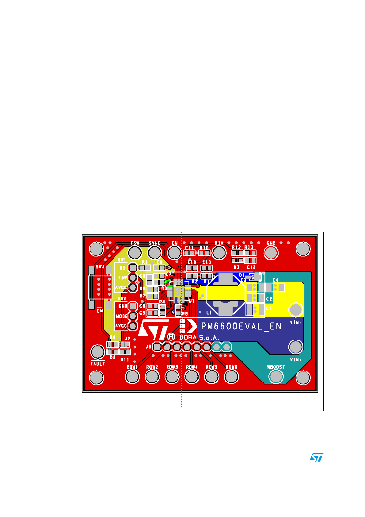
A.7 Top layer of the standard PM6600 demonstration board
While referring to the PM6600EVAL_EN demonstration board, the PGND and SGND
connections are more than one. In this case the PGND and SGND areas are separated in
the top layer (see Figure 1), while the bottom layer of the demonstration board is a unique
GND plane connected to SGND and PGND with the vias on the thermal pad and the vias
inside the test points.
Since the PM6600EVAL_EN demonstration board is an isolated system, there are no crosstalking issues between the GNDs areas.
When the device is mounted on a LCD board, together with other devices (digital, analog
and power ones), it is very important to properly follow the layout guidelines listed above, in
order to dedicate to each device the PGND and SGND portion of the entire board.
In the picture below:
● COMP > green
● Vin > dark blue
● LX > blue
● Vout > light blue
● PGND > light yellow
● SGND > dark yellow
Figure 54. Top layer critical signals components assembly and layout
Signal components Power components
46/60 Doc ID 14248 Rev 7

PM6600 Layout guidelines
The following pictures are the Gerber files of the PM6600EVAL_EN board.
Figure 55. Top side
1.1 cm
3 cm
Figure 56. Bottom side
Vias specs: diameter 0.8 mm, hole 0.3 mm
Doc ID 14248 Rev 7 47/60

Application note PM6600
Appendix B Application note
B.1 Inductor selection
Being the PM6600 mostly dedicated to notebook backlighting, real-estate applications
dictate severe constrain in selecting the optimal inductor. The inductor choice must take into
account different parameters like conduction losses (DCR), core losses (ferrite or ironpowder), saturation current and magnetic-flux shielding (core shape and technology).
The switching frequency of the PM6600 can be set in the 200 kHz-1 MHz range, allowing a
wide selecting room for the inductance value. Low switching frequencies takes to high
inductance value, resulting in significant DCR and size. On the other hand, high switching
frequencies result in significant core losses. The suggested range is 4.7-22 µH, even if the
best trade off between the different loss contributions varies from manufacturer to
manufacturer.
A 6.8 µH inductor has been experimentally found as the most suitable for applications
running at a 660 kHz switching frequency.
B.2 Capacitors selection
The input and output capacitors should have very low ESR (ceramic capacitors) in order to
minimize the ripple voltage. The boost converter of the PM6600 has been designed to
support ceramic capacitors. The required capacitance depends on the programmed LED
current and the minimum dimming frequency (the boost converter is off when the DIM pin is
low and the output capacitor is slowly discharged). Considering the worst case (i.e. 200 Hz
dimming frequency and 30mA/channel), two 2.2 µF MLCCs are suitable for almost all
applications. Particular care must be taken when selecting the rated voltage and the
dielectric type of the output capacitors: 50 V rated MLCC may show a significant
capacitance drop when biased, especially in case of Y5V dielectric.
As in most of boost converters, the input capacitor is less critical, although it is necessary to
reduce the switching noise on the supply rail. The input capacitor is also important for the
internal LDO of the PM6600 and must be kept as close as possible to the chip. The rated
voltage of the input capacitor can be chosen according to the supply voltage range; a 10 µF
X5R MLCC is recommended.
B.3 Flywheel diode selection
The flywheel diode must be a Schottky type to minimize the losses. This component is
subject to an average current equal to the output one and must sustain a reverse voltage
equal to the maximum output rail voltage. Considering all the channels sinking 30 mA each
(i.e. 180 mA output current) and the maximum output voltage (36 V), the STPS1L40M
(I
= 1 A, Vr = 40 V) diode is a good choice. Smaller diodes can be used in applications
f,ave
involving lower output voltage and/or lower output current.
48/60 Doc ID 14248 Rev 7

PM6600 Application note
(
B.4 Design example
In order to help the design of an application using the PM6600, in this section a simple stepby-step design example is provided.
A typical application could be the LCD backlight in a 14.1” LCD panel using the PM6600.
Here below the possible application conditions are listed:
● V
● 6 ROWs x 8 WLEDs @ 20 mA
● V
B.4.1 Switching frequency setting
To reduce the number of the external components, the default switching frequency is
selected (660 kHz typ.) by connecting the FSW pin to AVCC pin.
However, in case a different switching frequency is required, a resistor from FSW pin and
ground can be connected, according to the equation
Equation 22
= 12 ± 20%
IN
= 3.5 V ± 200 mV
F, L ED s
R
FSW
F
SW
=
5.2
B.4.2 Row current setting
The ROWs current is set using a resistor connected to the RILIM pin of the device. The
R
resistor can be calculated as:
RILIM
Equation 23
B.4.3 Inductor choice
The boost section, as all DC-DC converters, can work in CCM (continuous conduction
mode) or in DCM (discontinuous conduction mode) depending on load current, input and
output voltage and other parameters, among which the inductor value.
In a boost converter it is usually preferable to work in DCM.
Once the load, the input and output voltage, and the switching frequency are fixed, the
inductor value defining the boundary between DCM and CCM operation can be calculated
as:
Equation 24
R
RILIM
L
K
I
ROW
B
R
0
=
V998
mA20
2
)
−⋅⋅
D1DR
⋅
F2
SW
Ω=== k9.49
where D is the duty-cycle defined as:
Doc ID 14248 Rev 7 49/60

Application note PM6600
=⋅=
=+⋅
=
(
)
μ=<
Equation 25
=
⎧
V
IN
V
OUT
=−=
⎨
⎩
1D
min,IN
max,IN
V6.9V@68.0
=
V4.14V@52.0
whereas R0 is:
Equation 26
V
R
OUT
0
I
OUT
Ω== 250
and
Equation 27
ROWOUT
mA120I6I
The output voltage in the above calculations is considered as the maximum value (LED with
the maximum forward voltage connected to the leading generator):
Equation 28
max,LEDs,Fmax,OUT
V30mV400V8V
Figure 57. Inductor current in DCM operation
I
I
L
L
I
I
L, p eak
L, p eak
t
T
T
ON
ON
T
T
OF F
OF F
TSW= 1/F
TSW= 1/F
SW
SW
t
Considering the input voltage range, the lower LB will be at the lower input voltage. Hence
the condition to assure the DCM operation becomes:
Equation 29
min,INB
H2.13VLL
An inductor value of 6.8 µH could be a suitable value, considering also a margin from the
boundary condition.
50/60 Doc ID 14248 Rev 7

PM6600 Application note
(
)
It is important to highlight that the inductor choice involves not only the value itself but the
saturation current (higher than the boost current limit), the rated RMS current (the
compliance with the saturation current might be not enough; also the thermal performances
must be taken into account), the DCR (which affects the efficiency) and the size (in some
application might be a strict requirement).
However the DCR can’t be reduced keeping the size small. Hence a trade off between these
two requirements must be achieved according to the application.
B.4.4 Output capacitor choice
The choice of the output capacitor is mainly affected by the desired output voltage ripple.
Since the voltage across the LEDs can be considered almost constant, this ripple is
transferred across the current generators, affecting their dynamic response.
The output ripple can be estimated as (neglecting the contribution of ESR of C
in case of MLCC):
Equation 30
⋅−
TII
OFFOUTpeak,L
OUT
where I
=Δ
V
OUT
is the inductor peak current (see Figure 1) calculated as:
L, peak
⋅
C2
Equation 31
V6.9V@A044.1
I
peak,L
sw
=
⎨
⋅
LF
⎩
⎧
⋅
DV
IN
=
=
min,IN
V4.14V@A914.0
=
max,IN
whereas D, working in DCM, is:
Equation 32
=
⎧
−⋅⋅⋅
=
D
sw
R
0
)1M(MLF2
=
⎨
⎩
min,IN
max,IN
V6.9V@488.0
=
V4.14V@285.0
defining M as:
, very low
OUT
Equation 33
=
V6.9V@125.3
=
V4.14V@083.2
T
can be calculated as:
OFF
M
⎧
V
OUT
=
⎨
V
IN
⎩
min,IN
max,IN
Equation 34
⎧
=⋅=
DTT
⎨
2SWOFF
⎩
Doc ID 14248 Rev 7 51/60
=
min,IN
max,IN
V6.9V@ns5.348
=
V4.14V@ns5.398

Application note PM6600
(
)
defining D2 as:
V6.9V@23.0
=
D
2
SW
()
0
=
−⋅
1MR
⎨
⎩
⎧
⋅⋅⋅
MLF2
=
min,IN
V4.14V@263.0
=
max,IN
The worst case for the output voltage ripple is when input voltage is lower (V
A simple way to select the C
In order to affect as less as possible the current generators, it would be better to fix the
maximum ripple lower than the typical voltage across the generators.
For example considering ΔV
leading generator), the required capacitance is:
Equation 35
A margin from the calculated value should be taken into account because of the
capacitance drop due to the applied voltage when MLCCs are used.
A 4.7 µF MLCC can be a good choice for this application (two 2.2 μF MLCC in parallel can
be also a good solution).
In case a dimming duty cycle different from 100% is used, a further contribution to the
capacitor discharge (during the off time of the dimming cycle) should be considered.
B.4.5 Input capacitor choice
The input capacitor of a boost converter is less critical than the output capacitor, due to the
fact that the inductor is in series with the input, and hence, the input current waveform is
continuous.
IN,min
value is fixing a maximum voltage ripple.
OUT
lower than 80 mV (i.e. the 20% of the voltage across the
OUT
TII
⋅−
C
>
OUT
V2
Δ⋅
OFFOUTpeak,L
max,OUT
F02.2
μ=
= 9.6 V).
A low ESR capacitor is always recommended.
A capacitor of 10 µF is tentatively a good choice for most of the applications.
B.4.6 Overvoltage protection divider setting
The overvoltage protection (OVP) divider provides a partition of the output voltage to the
OVSEL pin. The OVP divider setting not only fixes the OVP threshold, but also the openchannel detection threshold (93% of the OVP threshold).
The proper OVP divider setting can be calculated by the equation:
Equation 36
52/60 Doc ID 14248 Rev 7
V
⎛
OVP
RR
⎜
21
235.1
⎝
−= 1
⎞
⎟
⎠

PM6600 Application note
+<<
+
=+⋅
=
V
has to be chosen in the range
OVP
Equation 37
Where
Equation 38
R1 can be chosen is in the order of hundreds of kilo-ohms to reduce the leakage current in
the resistor divider. For example, setting R
The OVSEL divider capacitors should be chosen according to the formula
Equation 39
For most cases, C10 = 220 pF and C13 = 22 pF are recommended.
B.4.7 Compensation network
For the compensation network, the suggestions provided in section 7.4 are always valid.
The following value of R3 and C8 are usually a good choice for the loop stability:
maxOUTOVPmaxOUT
maxWLED_Fseries_WLEDmaxOUT
= 15 kΩ leads to R1 = 390 kΩ (V
2
R
C5.1C ⋅⋅=
2
1013
R
1
V5.4VVV3V
V30mV400VnV
= 33.5 V).
OVP
R
= 2.4 kΩ
3
C
= 4.7 nF
8
These values are correct when working with 6 ROWs. For applications using less then 4
ROWs it is recommended to calculate again the value of the compensation components.
Please refer to the
B.4.8 Boost current limit
The boost current limit is set to protect the internal power switch against excessive current.
The slope compensation may reduce the programmed current limit. Hence, to take into
account this effect, as a rule of thumb, the current limit can be set as twice as much the
maximum inductor peak current (see section 1.2.4):
I
BOOST, PEAK
Therefore choosing I
Equation 40
Table 11 on page 54 for a detailed components check
> 2.09 A
BOOST, PEAK
= 2.5 A, R
R
BILIM
I
BILIM
K
B
PEAK,BOOST
will be:
Ω== k240
Doc ID 14248 Rev 7 53/60

Application note PM6600
B.4.9 Soft-start
The SS duration is set connecting a capacitor between the SS pin and GND. The capacitor
is thus charged with a constant 5 μA current, forcing the SS pin voltage to ramp up.
The current limit of the internal power-MOS is proportionally released. It reached the set
value when the voltage on the SS pin is 1.2 V.
During the initial part of the SS, the switching frequency is reduced to half of the set value.
This is done to avoid current runaway due to the minimum on time of the switching
controller. The switching frequency becomes the set one when the SS pin voltage is 0.8 V.
Since the current limit is been released proportionally, the changing of the switching
frequency causes the output to increase with an higher slew-rate.
In order to avoid the output overshoot and to avoid a too high slew rate in the OVSEL pin
voltage ramp, it is necessary to set up correctly the SS capacitors, taking into account all the
, I
, C
working conditions (mainly V
IN
OUT
During the SS it is performed the floating ROWs detection.
When one or more ROWs are open, the output voltage increases until the OVSEL pin
reaches the FRD threshold (93% of the OVP threshold). At this point the floating ROWs are
internally excluded from the control loop and considered not connected.
When the SS pin reaches 2.4 V all the IC protections turn active. The latched OVP
protection is activate as soon as the internal LDO regulates 5 V.
OUT
, ILIM)
In order to properly dimension the C
value, it should be considered the two cases: 6
SS
ROWs application and less than 6 ROWs application.
When working with 6 ROWs, the C
Since the DIM signal is internally forced to 100% during the soft-start, a bigger C
value should be chosen in the range 3.3 nF to 10 nF.
SS
results
SS
in a bigger WLEDs brightness that can be higher than the resultant one after the soft-start,
when the ROWs current generators are driven with the applied external DIM signal.
When working with less than 6 ROWs, the application components should be chosen in
order to avoid an OVP triggering due to the switching frequency change mechanism when
SS = 0.8 V. The suggested minimum value for C
is, in this case, 6.8 nF.
SS
Moreover, the other critical components to change respect to the standard 6 ROWs
application are
Table 11. Components
Component name 6 ROWs application < 6 ROWs application
C
SS
R
BILIM
R
SLOPE
R
COMP
C
COMP
CSS, R
BILIM
and R
components are changed to shift the time in which the frequency
SLOPE
increases at the set value. The shift guarantees to avoid any V
V
> 10 V.
IN
R
COMP
and C
are changed to lower the amplitude of the overshoot for 7.5 V<VIN<10 V.
COMP
3.3 nF 6.8 nF
250 kΩ 200 kΩ
680 kΩ 1 MΩ
2.4 kΩ 3.3 kΩ
4.7 nF 3.3 nF
overshoot with
OUT
This avoids the occurrence of the latched OVP condition.
54/60 Doc ID 14248 Rev 7

PM6600 Application suggestions
Appendix C Application suggestions
C.1 Full application schematic
Figure 58. Full application schematic
FAULT
VIN+
VIN -
EN
DIM
Ren 2
100kR
1
1kR t o 3.3kR
2
AVCC
Rdim1
Ren1
3.3kR
MODE
Cen
470nF
Rdi m 2
10 0 k R
L
Cin
>4 . 7 uF
AVCC
Cavcc
6
100nF
Cldo5
Rc o mp
Css
3.3nF to 10nF
2. 4 k R
SW3
Ccomp
3.3nF
330k
Rfsw
AVCC
Rf ilt
4.7R
7
LD O 5
1u F
22
FAULT
21
EN
20
DI M
5
MO D E
1
COM P
24
SS
AV CC
SW2
FSW
6.8uH to 15uH
23
8
VIN
SYNC
PM6600
FSW4RI L IM2BIL IM3SGND
Rb ilim
Rr ilim
180kR
50kR
OVSEL
SLO PE
19
LX
PGND
ROW6
ROW5
ROW4
ROW3
ROW2
ROW1
TH P D
10
18
9
17
16
15
14
13
12
11
25
D
STPS1L40M
ROW6
ROW5
ROW4
ROW3
ROW2
ROW1
C13
R1
22pF to 100pF
*
C10
R2
*
220pF to 1nF
Crow2 Crow4Crow3
Crow1
Crowx = 100pF to 470pF
Rs lop e
68 0 k R
Crow6Crow5
VBOOST
Cout
>4.7uF
3
With respect to the Basic application circuit (see chapter1), some optional components are
added. Below the suggestions, section by section, on why and in which cases to add these
components.
Doc ID 14248 Rev 7 55/60

Application suggestions PM6600
C.2 EN, DIM path in production line
Normally, in production line, the LCD modules are connected to testing machines with long
wires. The VIN, EN and DIM signals are provided with automatic testing equipment, such as
relays and/or software controlled switches, that connects the dedicated power supplies to
the board.
The wires parasitic inductance can lead to voltage spikes conditions that can exceed the
device maximum absolute ratings, thus resulting in a device damage.
In order to filter the critical signals, the suggestion is to add an RC network between the
board connector and the device pin.
Figure 59. EN pin filter
EN
Ren2
100 kR
1
In case of the EN pin, the recommended power supply value is 3.3 V, and we also suggest
to use an RC low pass filter network with Ren1 = 3.3 kΩ, Cen = 470 nF.
Ren1
3.3kR
EN
Cen
470 nF
If the EN is not externally driven, the PM6600 has an internal pull-up that permits to turn the
device ON by leaving the EN pin floating. In case the external driving circuit is present, but it
is not guaranteed that it drives the EN pin to a logic “0”, an external pull-down resistor Ren2
is needed.
Figure 60. DIM pin filter
DIM
Rdim1
1kR to 3.3kR
DIM
Rdim2
10 0kR
2
In the production line, the DIM signal is provided by a common power supply/signal
generator to a set of LED driver boards under test. The use of long wires and relays can
provoke spikes on the DIM pin, with a voltage level higher than the absolute maximum
ratings of the device. In this case, the device is internally damaged and stops working
properly.
To protect the DIM pin of the PM6600 device, a resistor Rdim1 is needed. It prevents a large
inrush current flowing into the device in case the voltage spike is exceeding the absolute
maximum ratings.
In case the DIM signal is provided by a micro controller (in production line and/or in the final
application), a pull-down resistor Rdim2 can be needed. If the micro controller is not
powered, it is possible that the voltage on the DIM pin of the PM6600 device will go to a logic
high level, because of board noise or signals coupling. The pull-down resistor avoids this
issue.
56/60 Doc ID 14248 Rev 7

PM6600 Application suggestions
In case of the DIM pin, we suggest to use a function generator. In case of using a power
supply, it is preferable to use 3.3 V and the same RC filter as the EN pin.
For what concerns the VIN pin, it is already filtered by the input capacitors.
C.3 ROW pins protection
Figure 61. ROW pins protection
ROW6
ROW5
ROW4
ROW3
ROW2
ROW1
Crow2 Crow4Crow3 Crow6Crow5
Crow1
Crow x = 1 00pF to 4 70pF
In the production line, the most common way to test the LED Driver PCB is to connect it to
the LED Board using a Dummy LED Driver Board. The Dummy Board is connected to the
LED Driver PCB by using metal needles, while it is directly connected to the LED Board.
The metal needles contacts, in case the board is not turned off while mounting/removing,
can provoke a charge injection into the ROWs pins of the device, thus damaging it. The
external capacitors, chosen in the range 100 pF to 470 pF, limits the voltage spike on the
ROWs pins, avoiding the charge injection.
In order to limit the EOS induced stress on ROWx pins, 1 nF capacitor can be used. In this
working conditions, please consider that the minimum on time of the current generator is
increased, due to the external capacitors that reduce the current turn-on/off slew-rate.
The capacitors connected between the ROWs pins and SGND are also useful in case of
ESD discharge on the ROWs pins bigger than the device specifications.
C.4 Debug and measurements test points
The tests points used to check the functionality of the board during PCB assembly and/or in
the production line can be dangerous in case of not-protected ESD environment or in case
overvoltage or overcurrent, exceeding the absolute maximum ratings (AMR) of the device,
hits them.
3
The critical pins involved are the ROWx pins. In case a testing machine is connected with
needles on the ROWx pins test points, it can be possible that an ESD, exceeding AMR,
occurs or it is possible that the testing machine creates and overvoltage/overcharge
condition in the pin. In this case the device will result damaged.
The corrective action is to add, for every ROWx pin, 100 pF capacitor vs GND and to avoid
the test points on the ROWx pins if not strictly necessary.
Doc ID 14248 Rev 7 57/60

Application suggestions PM6600
C.5 Inductor choice
The inductor selection should be done according to the datasheet guidelines.
The choice of the inductor value is explained in the
page 49
.
Section B.4.3: Inductor choice on
Moreover, the inductor has to be properly dimensioned also according to the boost current
limit,
Section B.4.8: Boost current limit on page 53
When using low current rated inductors, the risk is to have the inductor saturating during the
soft-start sequence or even during operating mode.
In case of saturation during the soft-start, the device can go into OVP and latch off. If the
inductor is hard saturating, both in soft-start and in operating mode, the risk is to have the
LX pin exceed the absolute maximum ratings. In this condition, the device will switch using
the minimum on time of the boost controller, to avoid the output overcharge and to preserve
the leds from issues. If the saturation is prolonged, the inductor is behaving as a wire (the
inductance value will be extremely reduced). This will create inductor damage and/or device
damage because of overstress condition.
58/60 Doc ID 14248 Rev 7

PM6600 Revision history
11 Revision history
Table 12. Document revision history
Date Revision Changes
07-Dec-2007 1 Initial release
21-Jan-2008 2 Updated Ta bl e 4 , Ta bl e 5 and Table 6 on page 12
07-Apr-2008 3 Updated Section 3.3 on page 11 and Section 8.2 on page 38
Updated Section 3.3 on page 11 and Section 8.2 on page 38
20-Oct-2008 4
12-Feb-2009 5
29-Jun-2009 6 Updated Table 4 on page 10
18-Feb-2010 7 Updated Section C.3 on page 57
Added Section Appendix A on page 44, Section Appendix C on page
55
Added Figure 58 on page 55, Figure 60 on page 56, Section C.1 on
page 55, Section C.3 on page 57
Doc ID 14248 Rev 7 59/60

PM6600
Please Read Carefully:
Information in this document is provided solely in connection with ST products. STMicroelectronics NV and its subsidiaries (“ST”) reserve the
right to make changes, corrections, modifications or improvements, to this document, and the products and services described herein at any
time, without notice.
All ST products are sold pursuant to ST’s terms and conditions of sale.
Purchasers are solely responsible for the choice, selection and use of the ST products and services described herein, and ST assumes no
liability whatsoever relating to the choice, selection or use of the ST products and services described herein.
No license, express or implied, by estoppel or otherwise, to any intellectual property rights is granted under this document. If any part of this
document refers to any third party products or services it shall not be deemed a license grant by ST for the use of such third party products
or services, or any intellectual property contained therein or considered as a warranty covering the use in any manner whatsoever of such
third party products or services or any intellectual property contained therein.
UNLESS OTHERWISE SET FORTH IN ST’S TERMS AND CONDITIONS OF SALE ST DISCLAIMS ANY EXPRESS OR IMPLIED
WARRANTY WITH RESPECT TO THE USE AND/OR SALE OF ST PRODUCTS INCLUDING WITHOUT LIMITATION IMPLIED
WARRANTIES OF MERCHANTABILITY, FITNESS FOR A PARTICULAR PURPOSE (AND THEIR EQUIVALENTS UNDER THE LAWS
OF ANY JURISDICTION), OR INFRINGEMENT OF ANY PATENT, COPYRIGHT OR OTHER INTELLECTUAL PROPERTY RIGHT.
UNLESS EXPRESSLY APPROVED IN WRITING BY AN AUTHORIZED ST REPRESENTATIVE, ST PRODUCTS ARE NOT
RECOMMENDED, AUTHORIZED OR WARRANTED FOR USE IN MILITARY, AIR CRAFT, SPACE, LIFE SAVING, OR LIFE SUSTAINING
APPLICATIONS, NOR IN PRODUCTS OR SYSTEMS WHERE FAILURE OR MALFUNCTION MAY RESULT IN PERSONAL INJURY,
DEATH, OR SEVERE PROPERTY OR ENVIRONMENTAL DAMAGE. ST PRODUCTS WHICH ARE NOT SPECIFIED AS "AUTOMOTIVE
GRADE" MAY ONLY BE USED IN AUTOMOTIVE APPLICATIONS AT USER’S OWN RISK.
Resale of ST products with provisions different from the statements and/or technical features set forth in this document shall immediately void
any warranty granted by ST for the ST product or service described herein and shall not create or extend in any manner whatsoever, any
liability of ST.
ST and the ST logo are trademarks or registered trademarks of ST in various countries.
Information in this document supersedes and replaces all information previously supplied.
The ST logo is a registered trademark of STMicroelectronics. All other names are the property of their respective owners.
© 2010 STMicroelectronics - All rights reserved
Australia - Belgium - Brazil - Canada - China - Czech Republic - Finland - France - Germany - Hong Kong - India - Israel - Italy - Japan -
STMicroelectronics group of companies
Malaysia - Malta - Morocco - Philippines - Singapore - Spain - Sweden - Switzerland - United Kingdom - United States of America
www.st.com
60/60 Doc ID 14248 Rev 7
 Loading...