

®
Application Specific Discretes
ASD™
MAIN PRODUCT CHARACTERISTICS
PKC-136
PEAK CLAMP
V
V
DRM
BR
160Vdc
700Vdc
P 1.5W
FEATURES
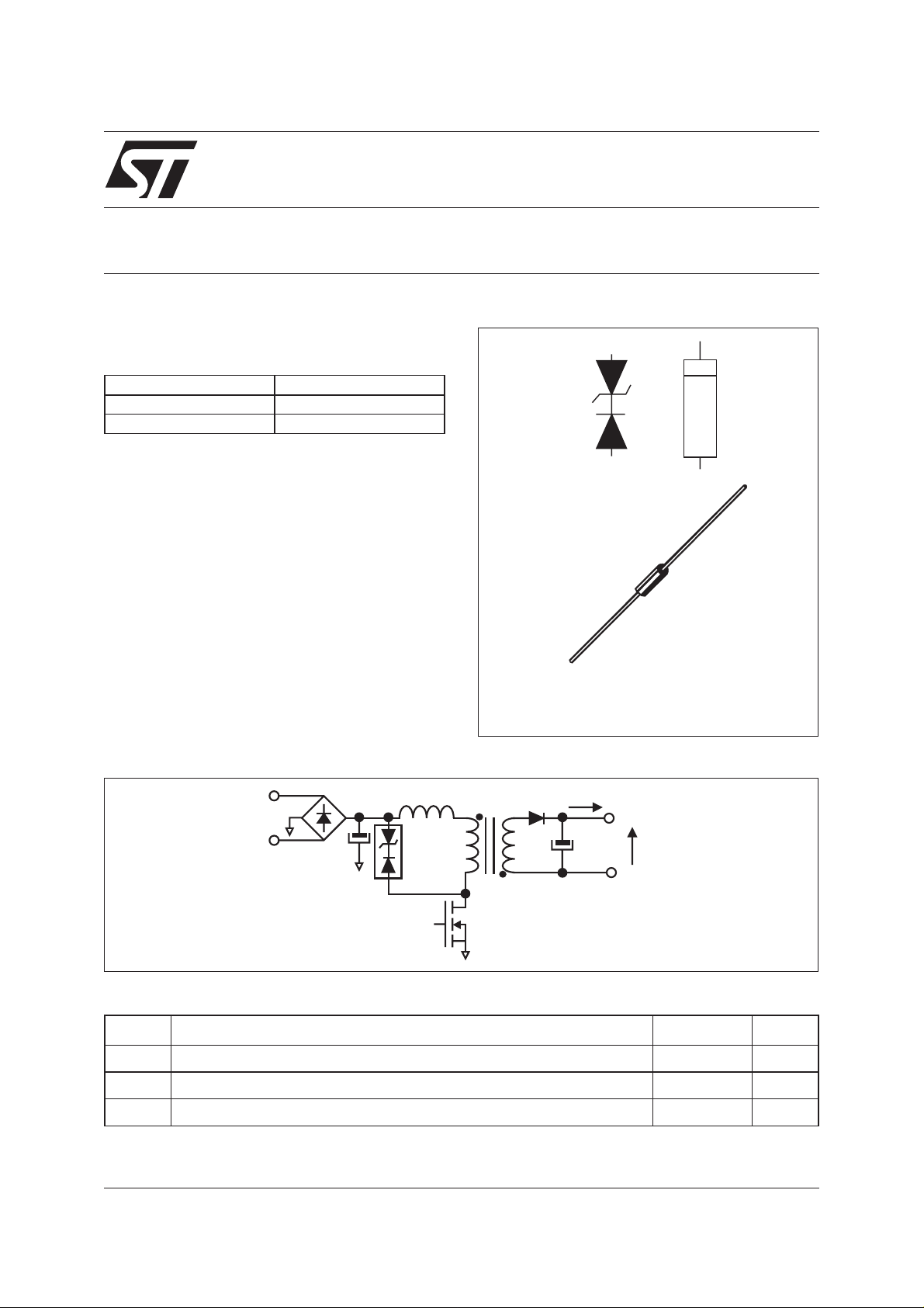
Protection of the Mosfet in flyback power supply
■
TRANSIL™ and blocking diode in a single
■
package
BENEFITS
Accurate voltage clamping regardless load
■
■ Reduced current loop
■ Reduced EMI emission
■ High integration
■
Fast assembly
■
Reduced losses in stand by mode
BASIC CONNECTION
Lf
DO-15
Io
T
D
Vo
ABSOLUTE MAXIMUM RATINGS (limiting values)
Symbol Parameter Value Unit
T
stg
Storage temperature
T
j
Junction temperature
P
August 2001 - Ed: 2A
Maximum power dissipation T°lead = 90°C
- 40 to + 150 °C
150 °C
1.5 W
1/5

PKC-136
ELECTRICAL CHARACTERISTICS TRANSIL
Symbol Parameter Test conditions
Unit
Min. Typ. Max.
Value
I
RM
V
BR
Leakage current VR= 136V
Breakdown voltage IR= 1mA
Tj= 25°C 1 µA
=125°C 10
T
j
Tj= 25°C 150 160 170 V
pulse test < 50ms
R
d
Dynamical Resistance tp < 500ns
Tj= 125°C 4 Ω
between I = 0.5Amps
and I = 1.5Amps
-4
αT
Temperature
10.8 10
/°C
Coefficient
V
sCL
Surge Clamping
voltage
Ipp = 2.7Amps
10/1000µs
219 V
CALCULATION OF THE CLAMPING VOLTAGE:
In repetitive mode and for low current rating, use the equation (1) and (2) to calculate the breakdown
voltage V
of the transil versus the operating junction temperature and use the equation (3) to calculate
BR
the clamping voltage versus the transil current Ipp and the temperature.
VTTVC
=− °α()()25 25
∆
BR j BR
VT V C V
() ( )=°+25 ∆
BR j BR BR
(1)
(2)
V T V T Rd Ipp
() () .=+
CL j BR j
(3)
ELECTRICAL CHARACTERISTICS DIODE (Tj = 25°C unless otherwise specified)
Value
Symbol Parameter Tests conditions
Min. Typ. Max.
I
R
V
RRM
Reverse leakage current VR=V
Repetitive Peak Reverse
Tj= 25°C
RRM
Tj= 25°C
= 125°C
T
j
320
700 V
3 µA
Voltage
trr
Reverse Recovery Time I
=1A dIF/ dt = -50A/µs
F
45 ns
VR= 30V
V
FP
Peak Forward Voltage IF=3A
dIF/ dt = 100A/µs
Tj= 25°C
= 125°C
T
j
12 V
18
CAPACITANCE
Symbol Parameter Typical Value Unit
C
Total Parasitic capacitance 1MHz 30mV
35 pF
Unit
2/5

PKC-136
THERMAL RESISTANCES
Symbol Parameter Value Unit
R
R
th(j-l)
th(j-a)
Junction to leads L = 10mm
Junction to ambiant condition see note 1
Note 1: Device mounted on a epoxy FR4 board of 35µm thickness
Lead Length: 10mm
Pad diameter: 4mm
Track width: 1mm
Track length: 25mm
The Rth
S(Cu) = 1.5cm
S(Cu) = 3.5cm
Fig.1:Peakpulse power versusexponentialpulse
duration.
1.E+02
1.E+01
1.E+00
1.E-01
1.E-04 1.E-03 1.E-02 1.E-01 1.E+00 1.E+01
can be reduced by replacing the Cu track by plan:
(j-a)
2
Pp(kW)
/lead R
2
/lead R
th(j-a)
th(j-a)
tp(ms)
= 65°C/W
= 60°C/W
Tj initial=25°C
Fig. 2: Relative variation of peak pulse power
versus initial junction temperature.
%
110
100
90
80
70
60
50
40
30
20
10
0
0 25 50 75 100 125 150 175
40 °C/W
105 °C/W
Tj(°C)
Fig. 3: Average power dissipation versus ambient
temperature.
P(W)
1.8
1.6
1.4
1.2
1.0
0.8
0.6
0.4
0.2
0.0
0 25 50 75 100 125 150
Tamb=Tleads
Printed circuit board
Tamb(°C)
Fig. 4: Variation of thermal impedance junction to
ambient versus pulse duration (printed circuit
board epoxy FR4)
Zth(j-a) (°C/W)
1000.0
Free air
100.0
10.0
tp(s)
1.0
1.E-02 1.E-01 1.E+00 1.E+01 1.E+02 1.E+03
3/5

PKC-136
Fig. 5: Thermal resistance junction to ambient
versus copper surface under each lead.
Rth(j-a)
110
100
90
80
70
60
50
40
30
20
10
0
012345678910
S(cm²)
Lleads=10mm
Fig. 6-2: Reverse leakage current versus reverse
voltage applied (typical values, for diode).
IR(µA)
1.E+02
1.E+01
1.E+00
1.E-01
1.E-02
1.E-03
0 50 100 150 200 250 300 350 400 450 500 550 600 650 700
Tj=150°C
Tj=125°C
Tj=100°C
Tj=25°C
VR(V)
Fig. 6-1: Reverse leakage current versus reverse
voltage applied (typical values, for Transil).
IR(µA)
1.E+00
1.E-01
1.E-02
1.E-03
1.E-04
1.E-05
Tj=150°C
Tj=125°C
Tj=100°C
Tj=25°C
VR(V)
1.E-06
10 20 30 40 50 60 70 80 90 100 110 120 130 140 150
Fig. 7: Transient peak forward voltage versus
/dt (90% confidence).
d
IF
V (V)
FP
50
IF=3A
Tj=125°C
45
40
35
30
25
20
15
10
5
0
0 50 100 150 200 250 300 350 400 450 500
dIF/dt(A/µs)
Fig. 8: Clamping voltage versus peak pulse
current (maximum values).
Ipp(A)
10.0
tp<500ns
Tj=25°C
1.0
Vcl(V)
0.1
160 165 170 175 180 185 190 195 200 205 210 215 220
4/5
Tj=125°C
Fig. 9: Junction capacitance versus reverse
voltage applied on clamping characteristic (typical
values).
C(pF)
100
VR(V)
10
1 10 100 1000
F=1MHz
Vosc=30mV
Tj=25°C
RMS

PACKAGE MECHANICAL DATA
DO-15
PKC-136
REF. DIMENSIONS
A
CC
Millimeters Inches
Min. Max. Min. Max.
A 6.05 6.75 0.238 0.266
B 2.95 3.53 0.116 0.139
D
B
C 26 31 1.024 1.220
D 0.71 0.88 0.028 0.035
Ordering type Marking Package Weight Baseqty
PKC136 Partnumber
DO-15 0.4g 1000 Ammopack
Diode cathode ring
PKC136-RL Partnumber
DO-15 0.4g 6000 Tape and reel
Diode cathode ring
Delivery
mode
Informationfurnished isbelieved tobeaccurate andreliable. However,STMicroelectronics assumes noresponsibility forthe consequences of
useof suchinformation norfor anyinfringementof patentsor otherrights ofthird parties whichmay resultfrom itsuse. No licenseis grantedby
implication or otherwise under any patent or patent rights of STMicroelectronics. Specifications mentioned in this publication are subject to
change withoutnotice. This publication supersedesand replaces all information previously supplied.
STMicroelectronics products are not authorized for use as critical components in life support devices or systems without express written approval ofSTMicroelectronics.
The ST logo is a registered trademark of STMicroelectronics
© 2001 STMicroelectronics - Printed in Italy - All rights reserved.
STMicroelectronics GROUP OF COMPANIES
Australia - Brazil - China - Finland - France - Germany - Hong Kong - India - Italy - Japan - Malaysia
Malta - Morocco - Singapore - Spain - Sweden - Switzerland - United Kingdom - U.S.A.
http://www.st.com
5/5
 Loading...