

查询STLC60444供应商
PeakSHDSL 8 CHANNEL CENTRAL OFFICE CHIPSET
DESCRIPTION
The 8-channel SHDSL chipset from S TM icroelectronics provides a complete low-power, low cost
solution for Central Office (CO) SHDSL solutions.
The chipset integrates all SHDS L functions from
Utopia interface to the line in three devices:
■ STLC80815: 8 channel SHDSL data pump
(SHDSL Transceiver)
■ STLC60444: 4 channel SHDSL Analog front
end
■ TS615: Dual wide band operational amplifier
with high output current
The product is targeted for customers looking to
build cost effective central office sol utions, i ncluding Digital Subscriber Line Access Multiplexers
(DSLAM) and Digital Loop Carriers (DLC).
PeakSHDSL
PRODUCT BRIEF
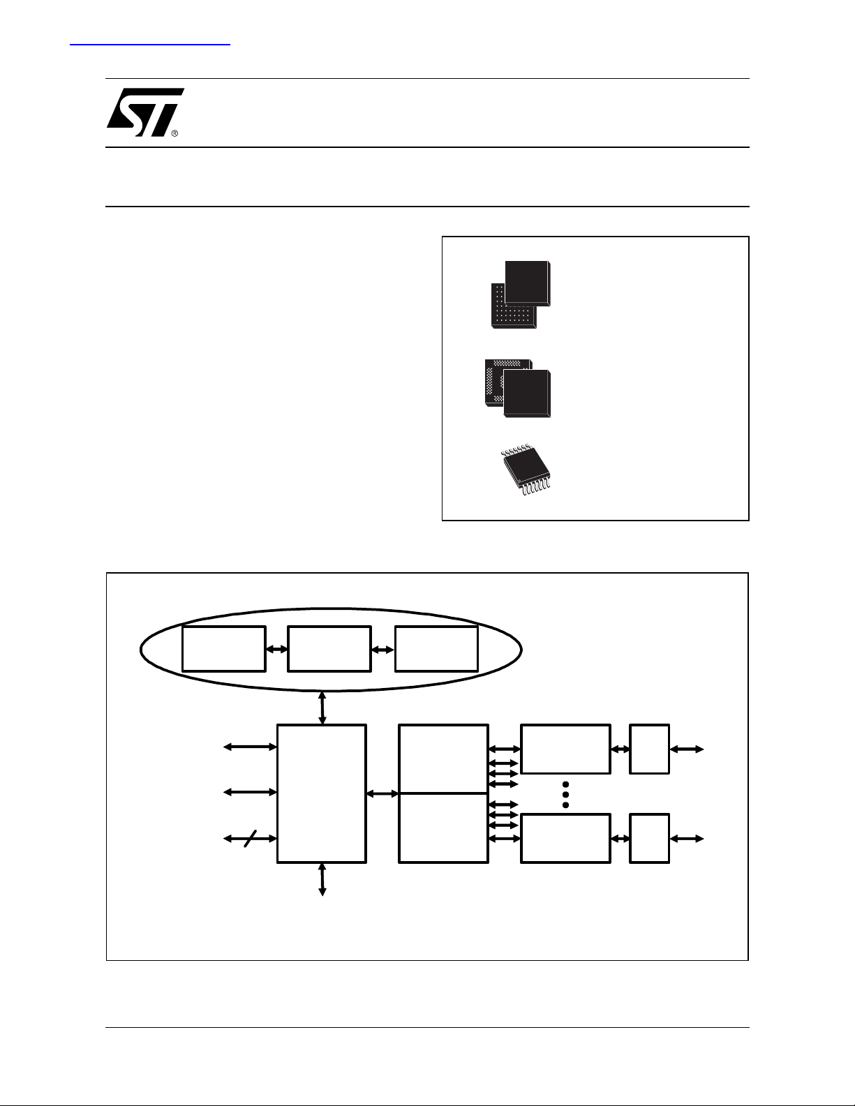
PBGA-272 package
for
STLC80815 device
EFBGA216 package
for
STLC60444 device
TSSOP14 package
for
TS615 device
CHIPSET ARCHITECTURE OVERVIEW
Figure 1. Chipset Architecture Overview
Flash ROM Host CPU SDRAM
Utopia
ATM
Octal SHDSL
PCM Highway
8
transceiver
PCM
Serial boot & management interface
Quad SHDSL
AFE
Quad SHDSL
AFE
Line driver &
hybrid
Line driver &
hybrid
Line
I/F
Line
I/F
Loop
Loop
With less than 750 mWatt per chan nel, the Pe akSHDSL chi ps et is one of the mo st com petitive s olutions
for SHDSL central office applications.
May 2003
This is preliminary information on a new product now in development. Details are subject to change without notice.
1/8

PeakSHDSL
STLC80815- 8 CHANNEL SHDSL DATA PUMP (SHDSL TRANSCEIVER)
Introduction
The STLC80815 includes eight indep endent transceive rs, which are optimized for central office application of Symmetrical Digital Subscriber Line (SHDSL) modems. The channels can operate simultaneously
in different modes and standards. It is an ideal integrated solution for central office equipment sensitive to
cost, power and space.
It includes full object code for a complete management/control and diagnostic API, and requires only power up initialization from the host interface. This allows a single low-cost host processor to supports tens of
ports via a parallel or serial interface.
A "hostless" line card can be designed using the STLC80815. In this case a remote host can boot the chip
and manage it via a serial host interface or using the in-band ATM cells.
Each channel in this highly integrated device includes the following components : frame, a PAM receiver
and transmitter, a 512 state TCM decoder and a timing synthesizer. In addition the device includes a centralized controller, which reduces to a minimum the requirements placed from the host, a Utopi a and a
PCM highway interface, which are common to all eight channels.
Figure 2. Block diagram of the STLC80815 SHDSL transceiver
Bitpump
(G.991.2
PCM x 8
PCM HW
NTR
PCM
TC
xDSL
Framer
(G.991.2
PMS-TC)
TPS-TC)
Modulator
Echo
Canceller
AFE Data
AFE
I/F
AFE Control
2/8
Utopia
ATM
TC
TC
(G.991.2
TPS-TC)
Dedicated
Risc
Controller
DSP
Controller
512 states
TCM
Decoder
modulator
Host I/F
Host Serial I/F
De-
PLL
Host Parallel I/F
17.664MHz Clk

PeakSHDSL
Main features
■ Compatibility with: ITU G.991.2 (G.SHDSL), ITU G.994.1 (G.HS) and ETSI RE/TM-06011 (SDSL),
ANSI HDSL2 and HDSL4.
■ Supports four-wire operation
■ Extremely low power consumption per channel: <700mW for all ITU G.991.2 Annex B rates, masks and
loops.
■ Outstanding reach performance: Symmetrical rate of 1552kbps over 5.5 Km (18.0kft) for an ETSI
0.4mm cable.
■ Includes 512 states TCM decoder
■ Supports symmetrical rates from 192 kbps up to 2.3 Mbit/s in step of 8kbps
■ Includes an internal, flexible frequency synthesizer
■ Supports all G.991.2 clock modes, including synchronous and plesiochronous modes.
■ Support operation with NTR, External PLL or VCXO are not required
■ Includes a fully-featured flexible framer, which supports simultaneous ATM and PCM transmis sion
■ T1/E1 and in-band ISDN services are supported
■ Serial and parallel host interface
■
In-band ATM boot and management supporte d
■ Complete software control protocol stack/API
■ Boundary scan testing compliant to IEEE 1149.1 Join Test Action Group (JTAG)
■ 272-pin TPBGA272 package (27x27m m)
■ -40 to 85°C operation
3/8

PeakSHDSL
STLC60444- 4-CHANNEL SHDSL ANALOG FRONT END
Short introd uction
The STMicroelectronics STLC 60444 Q uad A FE incorporat es fou r comple te ana log front end s, optim ized
for Central Office (CO) ADSL and SHDSL modems. The device integrates high-resolution analog to digital
converters (ADC) and digital to analog converters (DAC), which combined with active filtering significantly
reduces the requirements place d on external compon ents. Th e STLC60444 Q uad AFE is i deal for cost,
power and board area sensitive CO equipment.
Figure 3. Block diagram of STLC60444 SHDSL Analog Front End
16
15
8
Tx/Rx
Channel
Voltage Reference
Tx1
Rx1
8
Tx/Rx data
Data Interface
16
Data Interface
15
Voltage Reference
Tx/Rx
Channel
OEN
16
Control
Interface
4
Serial
Control I/F
15
Tx/Rx
Channel
Voltage Reference
Sync
Clock
VCXO
Clock
Generator
VCXO Control
16
15
Voltage Reference
Tx/Rx
Channel
Main features
■ Integrates four complete full-rate ADSL/SHDSL analog front ends
■ Integrates all active circuits except transmit line drivers
■ Low power, 3.3V operation
■ Integrated analog filters and 15-bit A/D & D/A converters
■ Interpolation filtering to reduce transmit channel data rate
■ 0 to +48 dB PGA range for each receive channel
■ Excellent SFDR and input noise performance
■ 0.35µm CMOS technology with Triple Well
■ Industrial temperature range (-40 °C to +85 °C)
Tx2
Rx2
Tx3
Rx3
Tx4
Rx4
4/8

PeakSHDSL
TS615 - DUAL WIDE BAND OPERATIONAL AMPLIFIER WITH HIGH OUTPUT CURRENT
Short Introd uction
The TS615 is a dual operational amplifier featuring a high output current 410mA. The TS615 is ideally suited for xDSL applications. The device is designed for the high slew rates to support low harmonic distortion
and intermodulation.
Main features
■ Low Noise: 5.2nV/(Hz)
■ High Peak Output Current: 420mA
■ Very Low Harmonic and Intermodulation Distortion (IM2 = -86dBc)
■ High Slew Rate: 410V/µsec
■ Current Feedback Structure
■ 14 pins TSSOP package
PeakSHDSL OCTAL-QUAD EVALUATION BOARD
ST offers a 8-channel evaluation board (EVM) which includes the STLC80815 eight-port SHDSL DSP, two
STLC60444 four-port AFE, eight line drivers, channel interface and protection circuits. The board is available now.
1/2
The board includes the following Interfaces:
– FDC interface (see below)
– Two UTOPIA connectors
– PCM OSM connectors, which can be multiplexed to a selected channel.
–OSM NTR
– 5x50 Header, which is connected to various points in the circuit, including all the PCM channels
– Eight RJ45 connectors to the lines
The board uses +12V, 3.3V and 1.8V supply rails.
For your reference the block diagram of the board is provided below:
5/8

PeakSHDSL
Figure 4. Block Diagram of the PeakSHDSL Octal-Quad EVM
PCM
OSMConnectors
TxD
TxC
RxD
RxC
UTOPIA
TX-CON
UTOPIA
RX-CON
NTR
PCM
Channel
Selector
4
4
4
4
4
4
4
4
4
36
FDC
CON
PCM0
PCM1
PCM2
PCM3
PCM4
PCM5
PCM6
PCM7
PCM
HW
STLC80815
Octal DSP
MONITOR
MICTOR
PARALLEL DATA
Byte SYNC
SERIAL CONTROL
CLK
PARALLEL DATA
Byte SYNC
SERIAL CONTROL
CLK
STLC
60444
Quad
AFE
STLC
60444
Quad
AFE
Tx (differential)
Rx (differential)
LD Control
Tx (differential)
Rx (differential)
LD Control
Tx (differential)
Rx (differential)
LD Control
Tx (differential)
Rx (differential)
LD Control
Tx (differential)
Rx (differential)
LD Control
Tx (differential)
Rx (differential)
LD Control
Tx (differential)
Rx (differential)
LD Control
Tx (differential)
Rx (differential)
LD Control
8 CHANNEL
LINE INTERFACE
LDH
CH#A
LDH
CH#B
LDH
CH#C
LDH
CH#D
LDH
CH#E
LDH
CH#F
LDH
CH#G
LDH
CH#H
Line Connector
RJ45
RJ45
RJ45
RJ45
RJ45
RJ45
RJ45
RJ45
6/8
NTR
PCM
TxD
TxC
RxD
RxC
OSC
80815
PCM
Tx SYNC
Rx SYNC
18
POWER MEASURE OPTION
1.8V - OCTAVE
3.3V - OCTAVE
3.3V - SAIPH - DIGITAL
3.3V - SAIPH - ANALOG
80815
Host
ADDR
11
5x50 HEADEAR
(Optional)
+12V LD (1-8)
3.3V - DVCC
80815
Host
DATAUtopia
8
80815
ale, wr,
rd, cs
80815
serial
DUMP
interface
80815
serial
host
interface
P
O
W
E
R
C
O
N

PeakSHDSL
OCTAL CHIPSET, SOFTWARE AND REFERENCE DESIGN
The PeakSHDSL chipset consists of an octal digital Transceiver (STLC80815) and two quad AFEs
(STLC60444). These chips are part of a chipset with a number of user interfaces available including Utopia
level 2, Eight PCM (16 for the Hex solution), and PCM highway.
Software and Management is supported through:
– A complete software control protocol stack/API
– No need for real-time interaction with any host CPU
– Supports in-band ATM management and in-band boot through the Utopia interface
– Hostless line-card design using serial host i/f or in-band ATM
– Boundary scan testing compliant to IEEE 1149.1 Joint Test Action Group (JTAG)
The PeakSHDSL solution is provided via a fully documented, turnkey transceiver reference design, development systems, and technical support. This includes a development kit that allows customers to shorten
the designer's development time by quickly building complete SHDSL solutions:
–
A Hardware Design Guide - which includes transceiver schematics, transceiver layout gerbers and
bill of materials (BOM). The design guide also includes detail s on planning, layout, testing and debugging an SHDSL product.
–
A Software Design Guide - which includes a detailed description of the management protocol.
Moreover, ST offers the Host CPU Interface Library software code with instructions to help integrate
the software functions into the customer's source code.
–
Fast Debugger Card (FDC) and Man ager Analyzer T ools - To a ssist customers with evaluation,
test and debug of their SHDSL design at the early phase of development, ST offers the Fast Debugger Card (FDC) and Manager Analyzer Tools (OMANA, a MS-Windows® based PC application). Using these tools enables testing the SHDSL circuitry even before the host controller software is
completed, by bypassing the host using the FDC. The Manager Analyzer Tool enables the customer
to configure the SHDSL transceiver and test performance and provides a graphic display of system
performance.
–
The Profiler - to assist incorporating the interface l ib rary into t he host sof tware, ST provides the Pro-
filer. The Profiler is a PC based application that displays statistics on memory and real tim e requirements of the API task, the interrupt handler and the messages queues that are used. Using this tool
will scale the required memory b uffers and help id entify and sol ve real t ime issues during software
integration.
7/8

PeakSHDSL
Information furnished is believed to be accurate and reliable. However, STMicroelectronics assumes no responsibility for the consequences
of use of such information nor for any infringement of patents or other rights of third parties which may result from its use. No license is granted
by implic ation or otherwise under any patent or p at ent rights of STMicroelectronics. Spec i fications mentioned in this publicatio n are subject
to change without notice. This publication supersedes and replaces all information previously supplied. STMicroelectronics products are not
authorized for use as cri t i cal compone nts in life support device s or systems without express written approval of STM i croelectr onics.
STMicroelectronic s acknowledges the trad emarks of all companies re fe rred to in this document.
The ST logo is a registered trademark of STMicroelectronics
© 2003 STMic roelectronics - All Rig hts Reserved
Austra lia - Brazil - Canada - Ch i na - F i nl and - France - Germany - Hong Kong - In di a - I srael - Italy - J apan -Malaysia - Malta - Morocco -
Singap ore - Spain - Sweden - Switzerland - U ni ted Kingdom - United St at es.
STMicroelectronics GROUP OF COMPANIES
http://www.s t. com
8/8
 Loading...