


Features
P
■ EXCELLENT THERM AL STABILITY
■ COMMON SOURCE CONFIGURATION
■ BROADBAND PERFORMANCES P
WITH 15 dB GAIN @ 500MHz
■ NEW LEADLESS PLAST IC PAC KAG E
■ EDS PROTECTION
■ SUPPLIED IN TAPE & REEL OF 3K UNITS
■ IN COMPLIANCE WITH THE 2002/93/E C
EUROPEAN DIRECTIVE
OUT
= 8W
Description
The PD54008L-E is a common source
N-Channel, enhancement-mode lateral FieldEffect RF power transistor. I t is designed for high
gain, broad band commercial and industrial
applications. It operates at 7 V in comm on source
mode at frequencies of up to 1 GHz. PD54008L-E
boasts the excellent gain, linearity and reliability
of STH1LV latest LDMOS technology mounted in
the innovative leadless SMD plastic package,
PowerFLAT™.
PD54008L-E
RF Power Transistors
The LdmoST Plastic FAMILY
PowerFLAT™ (5x5)
in Connection
PD54008L-E’s superior linearity performance
makes it an ideal solution for portable radio.
TOP VIEW
Order Codes
Part Number Marking Package Packaging
PD54008L-E 54008 PowerFLAT (5x5) Tape & Reel
Rev 1
January 2006 1/15
www.st.com
15

PD54008L-E
Contents
1 Electrical Data . . . . . . . . . . . . . . . . . . . . . . . . . . . . . . . . . . . . . . . . . . . . . . . . 3
1.1 Maximum Ratings . . . . . . . . . . . . . . . . . . . . . . . . . . . . . . . . . . . . . . . . . . . . . . 3
1.2 Thermal Data . . . . . . . . . . . . . . . . . . . . . . . . . . . . . . . . . . . . . . . . . . . . . . . . . 3
1.3 Electrical Characteristics . . . . . . . . . . . . . . . . . . . . . . . . . . . . . . . . . . . . . . . . . 4
2 Impedances . . . . . . . . . . . . . . . . . . . . . . . . . . . . . . . . . . . . . . . . . . . . . . . . . . 5
3 Typical Performance . . . . . . . . . . . . . . . . . . . . . . . . . . . . . . . . . . . . . . . . . . . 6
3.1 Typical Performance (Broadband) . . . . . . . . . . . . . . . . . . . . . . . . . . . . . . . . . 7
4 Test circuit schematic . . . . . . . . . . . . . . . . . . . . . . . . . . . . . . . . . . . . . . . . . . 8
5 Package Mechanical Data . . . . . . . . . . . . . . . . . . . . . . . . . . . . . . . . . . . . . . 10
6 Revision History . . . . . . . . . . . . . . . . . . . . . . . . . . . . . . . . . . . . . . . . . . . . . 14
2/15
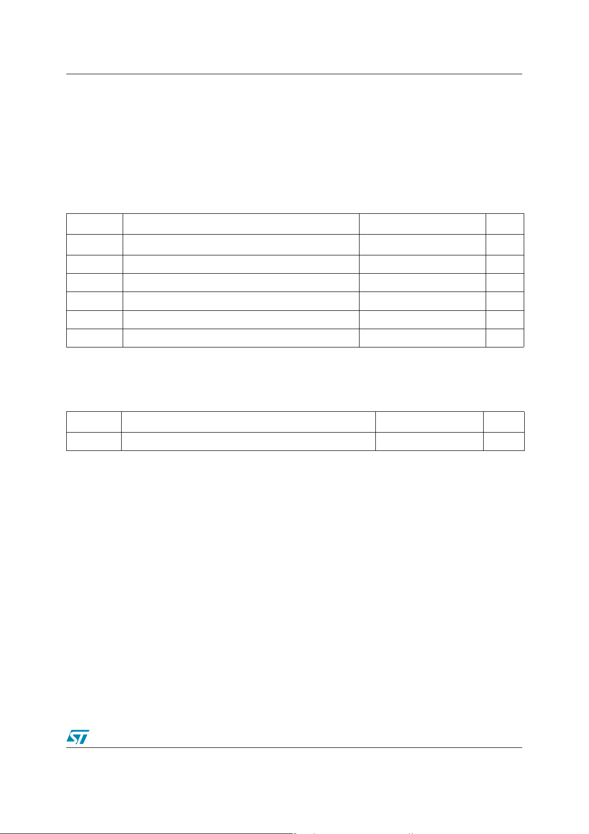
PD54008L-E 1 Electri c al Data
1 Electrical Data
1.1 Maximum Ratings
Table 1. Absolute Maximum Ratings
(T
Symbol Parameter Value Unit
V
(BR)DSS
V
GS
I
D
P
DISS
T
J
T
STG
= 25°C)
CASE
Drain Source Voltage 25 V
Gate-Source Voltage -0.5 to +15 V
Drain Current 5 A
Power Dissipation (t
Max. Operating Junction Temperature 150 °C
Storage Temperature -65 to +150 °C
case
=70°C)
26.7 W
1.2 Thermal Data
Table 2. Thermal data
Symbol Parameter Value Unit
R
thj-case
Junction to Case t hermal resistance 3 °C/W
3/15
1 Electrical Data PD54008L-E
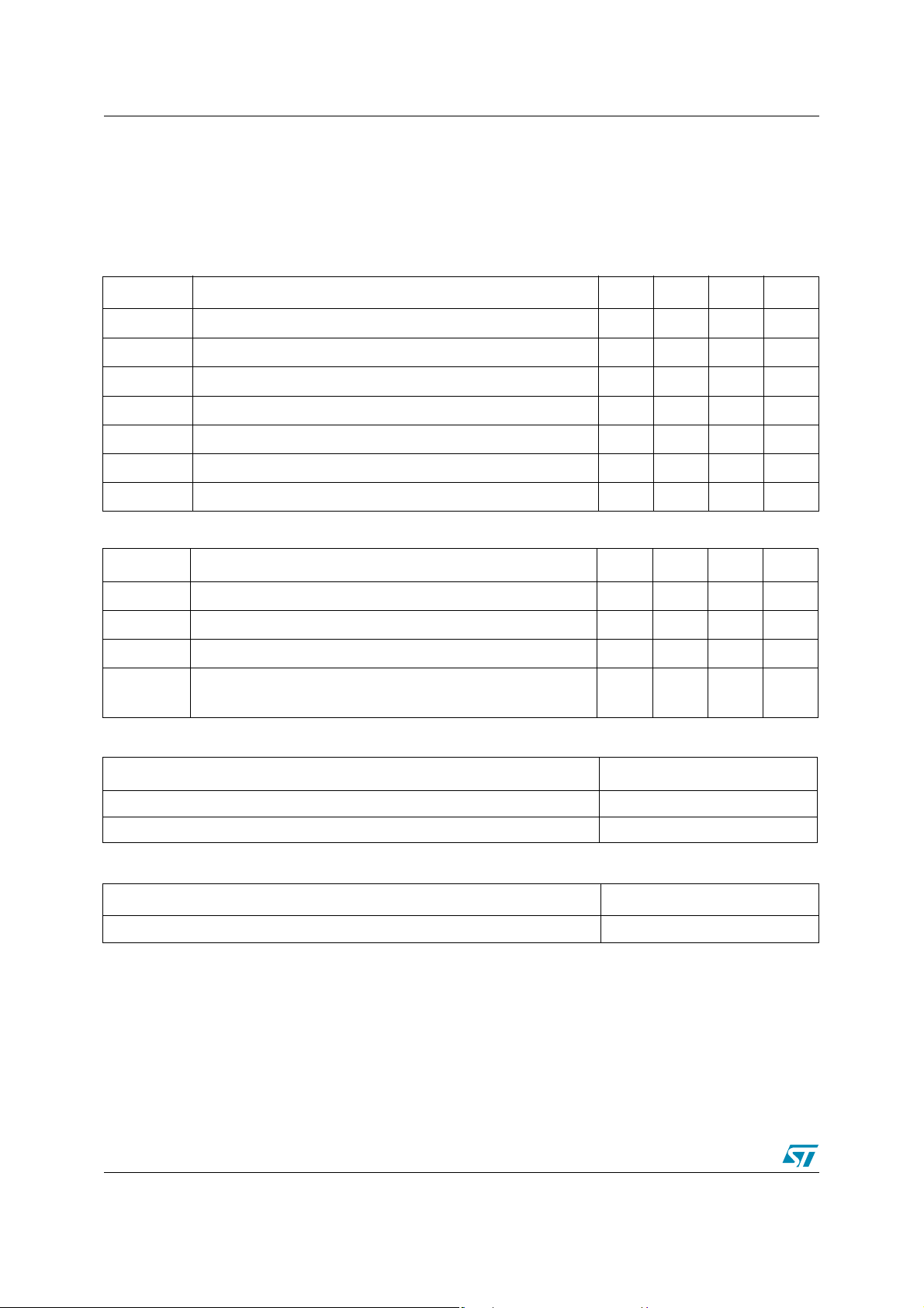
1.3 Electrical Characteristics
(T
CASE
= 25°C)
Table 3. Static
Symbol Test Conditions Min. Typ. Max. Unit
I
DSS
I
GSS
V
GS(Q)
V
DS(ON)
C
C
OSS
C
ISS
RSS
VGS = 0V VDS = 25V
VGS = 5V VDS = 0V
VDS = 10V ID = 50mA
VGS = 10V ID = 0.5A
VGS = 0V VDS = 7.5V f = 1MHz
VGS = 0V VDS = 7.5V f = 1MHz
VGS = 0V VDS = 7.5V f = 1MHz
1 μA
1 μA
2.0 5.0 V
0.09 V
80 pF
60 pF
6.6 pF
Table 4. Dynamic
Symbol T est Conditions Min. Typ. Max. Unit
P
1dB
G
PS
η
D
Load
Mismatch
VDD = 7.5 V IDQ = 200 mA f = 500MHz
VDD = 7.5 V IDQ = 200 mA P
VDD = 7.5 V IDQ = 200 mA P
V
= 7.5 V IDQ = 200 mA P
DD
8 W f = 500MHz
OUT =
= 8 W f = 500MHz
OUT
8W f = 500MHz
OUT =
All Phase Angles
8W
15 dB
50 %
20:1 VSWR
Table 5. ESD Protection Characteristics
T est Conditions Class
Human Body Model 2
Machine Model M3
Table 6. Moisture Sensitivity Level
Test Methodology Rating
J-STD-020B MSL 3
4/15

PD54008L-E 2 Impedances
2 Impedances
Figure 1. Impedance Data Schematic
D
Z
DL
Table 7. Impedance Data
f
SC13140
(1)
Typical Input
Impedance
G
Zin
Z
IN
(Ω)Z
S
Typical Drain
Load Impedance
480MHz 1.12 - j 2.02 2.01 + j 0. 13
500MHz 1.3 - j 2.01 1.84 + j 0.7
520MHz 1.66 - j 2.55 1.66 + j 1. 51
DL
(Ω)
1. In Broadband amp lif ier
5/15

3 T ypical Performance PD54008L-E
Vds = 7.5 V
Vds = 7. 5 V
Vds = 7.5 V
Ciss
3 Typical Performance
Figure 2. Power Gain vs. Output Power Figure 3. Efficiency vs Outpu t Power
20
Idq = 200 mA
19
18
17
16
15
Gp (dB)
14
13
12
11
10
Idq = 150 mA
Idq = 100 mA
f = 500 MHz
012345678910
Pout (W)
80
70
60
50
40
Nd (%)
30
20
10
0
012345678910
Pout (W)
Idq = 200 mA
f = 500 MHz
Figure 4. Return Loss vs. Ou t pu t Power Figure 5. Capacitance Vs S upp ly Voltage
0
-5
-10
-15
RL (dB)
-20
-25
Idq = 20 0 mA
f = 500 MHz
1000
f = 1 MHz
100
Coss
C (pF)
10
Crss
-30
012345678910
Pout (W)
6/15
1
0123456789
Vds (V)

PD54008L-E 3 Typical Perf ormance
3.1 Typical Performance (Broadband)
Figure 6. Power Gain vs. Frequency Figure 7. Efficiency vs. Frequency
14
12
10
8
Gp (dB)
6
4
2
0
470 480 490 500 510 520 530
f (MH z)
Idq = 150 mA
Pin = 26 dBm
Figure 8. Return Loss vs. Frequency
0
-4
-8
RL (dB)
-12
70
60
50
40
Nd (%)
30
20
10
0
470 480 490 500 510 520 530
f (MHz)
Idq = 150 mA
Pin = 26 dBm
-16
-20
470 480 490 500 510 520 530
f (MH z)
Idq = 150 mA
Pin = 26 dBm
7/15

4 Test circuit schematic PD54008L-E
4 Test ci rcuit schematic
Figure 9. Internal schematic
Table 8. Test circuit component part list
COMPONENT DESCRIPTION
B1, B2 Ferrite bead
C1, C16 300 pF, 100 mil ATC
C2, C3, C4, C13,C14 1 -:- 20 pF Trimmer cap - JOHANSON
C15 0.8 -:- 10 pF Trimmer cap - JOHANSON
C5 36 pF, 100 mil ATC
C6 51 pF, 100 mil ATC
C7 62 pF, 100 mil ATC
C8, C17 150 pF, 100 mil CHIP CAP
C9 1 nF, 100 mil CHIP CAP
C10, C18 1000 pF, 100 mil CHIP CAP
C11, C19 0.1 nF, 100 mil CHIP CAP
C12, C20 10 μF 50 V Electrolytic Capacitor
C21 15 pF, 100 mil ATC
L 43nH, Coilcraft
R1 33 KΩ, 1W CHIP Resistor
R3 1 KΩ, 1W CHIP Resistor
R4 15 Ω, 1W CHIP Resistor
Z1 0.49" X 0.080" MICROSTRIP
Z2 1.024" X 0.080" MICROSTRIP
Z3 0.079" X 0.080" MICROSTRIP
Z4 0.24" X 0.223" MICROSTRIP
Z5 0.079" X 0.223" MICROSTRIP
8/15

PD54008L-E 4 Test circuit schematic
Table 8. Test circuit component part list
Z6 0.138" X 0.223" MICROSTRIP
Z7 0.259" X 0.223" MICROSTRIP
Z8 0.079" X 0.080" MICROSTRIP
Z9 0.413" X 0.080" MICROSTRIP
Z10 0.756" X 0.080" MICROSTRIP
Z1 1 0.61" X 0.080" MICROSTRIP
N1, N2 Typ e N Flange Mount
Board ROGER, ULTRA LAM 2000 THK 0.030", εr = 2.55 2oz. ED cu SIDES
9/15

5 Package Mechani cal Data PD54008L-E
5 Package M echanical Da ta
In order to meet environmental requirements, ST offers these devices in ECOPACK®
packages. These packages have a Lead-free second level interconnect . The category of
second level interconnect is marked on the package and on the inner box label, in compliance
with JEDEC Standard JESD97. The maximum ratings related to soldering conditions are also
marked on the inner box label. ECOPACK is an ST trademark. ECOPACK specifications are
available at: www.st.com
10/15

PD54008L-E 5 Package Mechan ical Data
Table 9. PowerFLAT™ Mechanical Data
mm inch
Dim.
MIN. TYP. MAX. MIN. TYP. MAX.
A 0.90 1.00 0.035 0.039
A1 0.02 0.05 0.001 0.002
A3 0.24 0.009
AA 0.15 0.25 0.35 0.006 0.01 0.014
b 0.43 0.51 0.58 0.017 0.020 0.023
c 0.64 0.71 0.79 0.025 0.028 0.031
D 5.00 0.197
d 0.30 0.011
E 5.00 0.197
E2 2.49 2.57 2.64 0.098 0.101 0.104
e 1.27 0.050
f 3.37 0.132
g 0.74 0.03
h 0.21 0.008
Figure 10. PowerFLAT™ Package Dimensions
11/15

5 Package Mechani cal Data PD54008L-E
Table 10. PowerFLAT™ Tape & Reel Dimensions
mm.
DIM.
MIN. TYP MAX.
Ao 5.15 5.25 5.35
Bo 5.15 5.25 5.35
Ko 1.0 1.1 1.2
Figure 1 1. PowerFLAT™ T ape & Reel
12/15

PD54008L-E 5 Package Mechan ical Data
Table 11. Recommended FO OTPR IN T
13/15

6 Revision Hist ory PD54008L-E
6 Revision History
Date Revision Description of Changes
19-Jan-2006 1 First Issue
14/15

PD54008L-E 6 Revision History
I
s
o
d
b
ct
t
ot
a
nformation furnished is believed to be accurate and reliable. However, STMicroelectronics assumes no responsibility for the consequence
f use of such information nor for any infringement of patents or other rights of third parties which may result from its use. No license is grante
y implic ation or otherwise under any patent or patent ri ghts of STM i croelectr onics. Specifications menti oned in thi s publicati on are subje
o change without notice. This publication supersedes and replaces all information previously supplied. STMicroelectronics products are n
uthoriz ed for use as critical compo nents in life support devic es or systems without express writt en approval of STMicroel ectronics.
The ST logo is a registered t rademark of S TM i croelectr oni cs.
All other nam es are the pro perty of thei r respectiv e owners
© 2006 STMi croelectronics - All ri ght s reserved
Austra l i a - Be l gi um - Brazil - Canada - Chi na - Czech Rep ubl i c - Finland - F rance - Germ any - Hong Kon g - In di a - Israel - It aly - Japan -
Malaysi a - M al ta - Morocco - Singapore - Spain - Swe den - Switzerland - Un i te d Kingdom - United States of America
STMicroelectron ics group of com panies
www.st.com
15/15
 Loading...