

STEVAL-PCC009V4
STEVAL-PCC009V4
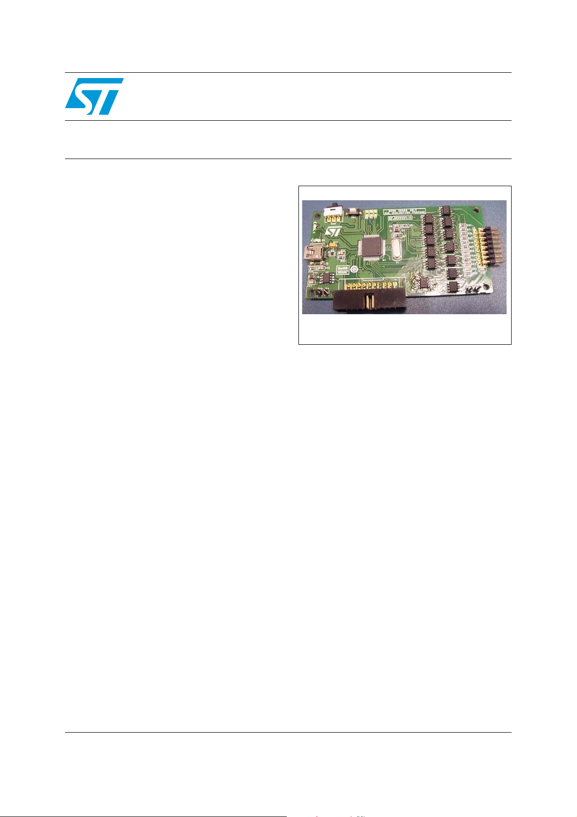
Opto-isolated universal USB to serial bridge demonstration board
for motor control applications
Data brief
Features
■ STM32-based demonstration board used as
the interface between the PC and motor control
systems
■ 8-pin interface for SPI/I
■ 6 GPIOs available
■ Opto-isolation on SPI, USART and GPIOs
■ Magnetic isolation for I
■ RoHS compliant
Description
The STEVAL-PCC009V4 demonstration board
implements a universal USB on the serial isolated
interface communication. It is useful in all
applications which need safe connection from PC
to the application boards.
2
C/UART
2
C
The STEVAL-PCC009V4 has a 16-pin
communication interface which allows connecting
a device that uses I
2
C, SPI or UART protocols.
Thus, the board functions as a bridge between a
serial communication based device and a PC.
July 2012 Doc ID 022310 Rev 2 1/8
For further information contact your local STMicroelectronics sales office.
www.st.com
8
Schematics STEVAL-PCC009V4
3V3
3V3
BOOT0
OSC_IN
RESET#
3V3
3V3
OSC_IN
RESET#
3V3
VDDA
AGND
PC8
OSC_OUT
OSC_OUT
AGND
VDDA
3V3
GND
3V3
GND
3V3
GND
3V3
BOOT1_PB2
BOOT1_PB2
3V3
3V3
GND
BOOT0
PB4_NTRST
PB3_TDO
PA15_TDI
PA14_TCK
PD2
USBDM
USBDP
PA13_TMS
PC5
PC4
PC8
PB9_TIM4_CH4
PB8_TIM4_CH3
PA3_USART2_RX
PA0_USART2_CTS
PC0_GPIO_IN10
PA6_SPI1_MISO
PA1_USART2_RTS
PB7_I2C1_SDA
PB6_I2C1_SCL
PB5_I2C1_SMBAI
PA7_SPI1_MOSI
PA5_SPI1_SCK
PA4_USART2_CLK
PA2_USART2_TX
R3
0
R3
0
C1
22pF
C1
22pF
C8
100nF
C8
100nF
R4
0
R4
0
C6
100nF
C6
100nF
L1
10uH
L1
10uH
SW1
SW _PB
SW1
SW _PB
C5
10nF
C5
10nF
R5
0
R5
0
R9
0
R9
0
C2
22pF
C2
22pF
D1
STATUS
D1
STATUS
R8
10k
R8
10k
R2
100k
R2
100k
R1
100k
R1
100k
Y1
8MHz
Y1
8MHz
R6
0
R6
0
C4
10uF
C4
10uF
C7
100nF
C7
100nF
R7
1M
R7
1M
C9
100nF
C9
100nF
U1
STM32F103RBT6
U1
STM32F103RBT6
PD2
54
PC12
53
PC11
52
PC10
51
PA1 5
50
PA1 4
49
VDD_2
48
VSS_2
47
PA1 3
46
PA1 2
45
PA11
44
PA1 0
43
PA9
42
PA8
41
PC9
40
PC8
39
PC7
38
PC6
37
VBAT
1
PC13-TAMPER-RTC
2
PC14-OSC32_IN
3
PC15-OSC32_OUT
4
PD0 OSC_IN
5
PD1 OSC_OUT
6
PC0
8
NRST
7
VSSA
12
PC1
9
VDD-4
19
PC2
10
PC3
11
VDDA
13
PA0 -W KUP
14
PA1
15
PA2
16
PA3
17
VSS_4
18
PA4
20
PA5
21
PA6
22
PA7
23
PC4
24
PC5
25
PB0
26
PB1
27
PB2
28
PB6
58
PB15
36
PB14
35
PB13
34
PB12
33
VSS_1
31
PB11
30
VDD_1
32
PB10
29
PB5
57
PB4
56
PB3
55
BOOT0
60
PB7
59
PB8
61
PB9
62
VSS_3
63
VDD_3
64
R10
360
R10
360
C3
100nF
C3
100nF
AM10181V1
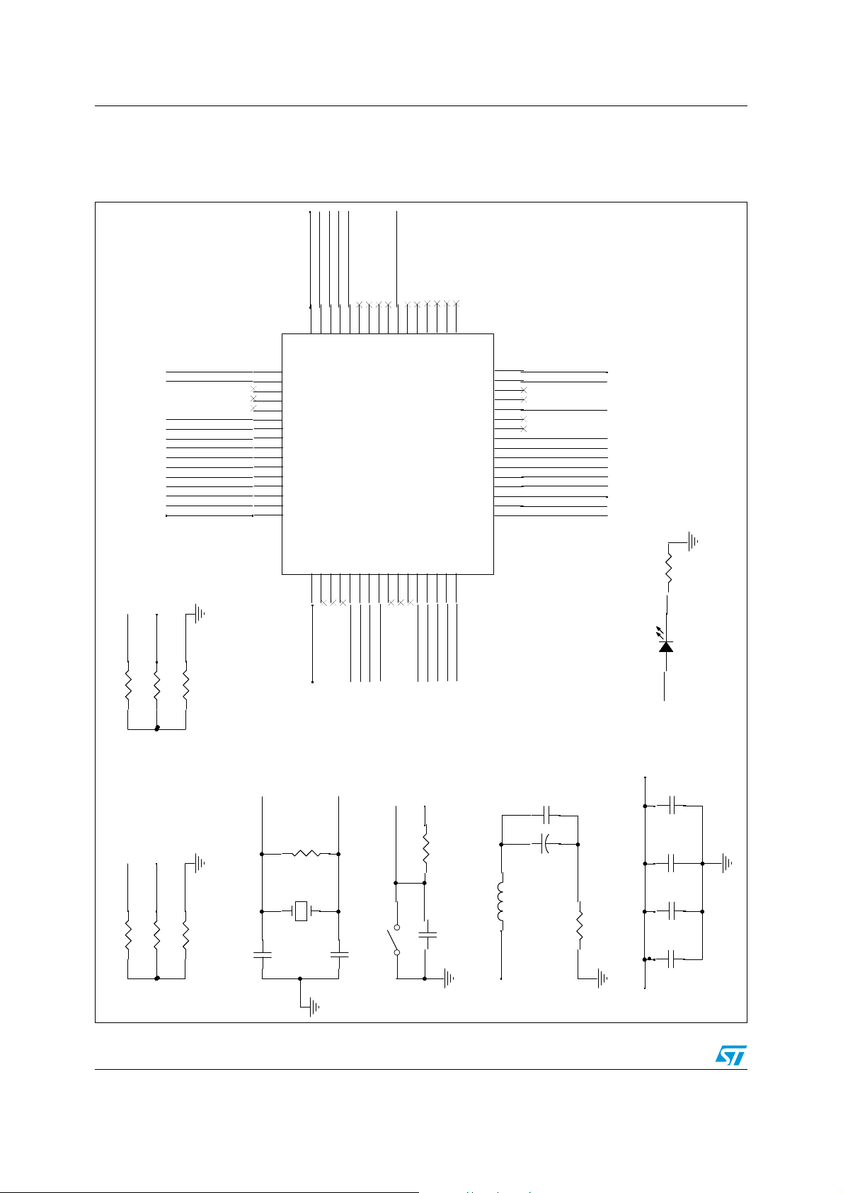
1 Schematics
Figure 1. Microcontroller section
2/8 Doc ID 022310 Rev 2
STEVAL-PCC009V4 Schematics
PB4_NTRST
PA15_TDI
PA13_TMS
3V33V3
PA14_TCK
PA13_TMS
PB4_NTRST
PA15_TDI
PB3_TDO
RESET#
3V3
PA14_TCK
R36
4k7
R36
4k7
R18
10k
R18
10k
R20
10k
R20
10k
R37
4k7
R37
4k7
R19
10k
R19
10k
R38
4k7
R38
4k7
R39
4k7
R39
4k7
R16
10k
R16
10k
J1
JTAG_20PIN
J1
JTAG_20PIN
12
34
56
78
910
1112
1314
1516
1718
1920
AM10182V1
PC5
3V3
3V3
PC5
VDD_TGND_T
TP3
TEST POINT
TP3
TEST POINT
1
TP1
TEST POINT
TP1
TEST POINT
1
C25
100nF
C25
100nF
SW2
MODE SELECTION SWITCH
SW2
MODE SELECTION SWITCH
3
2
1
TP2
TEST POINT
TP2
TEST POINT
1
R15
100
R15
100
TP4
TEST POINT
TP4
TEST POINT
1
R17
10k
R17
10k
AM10183v1
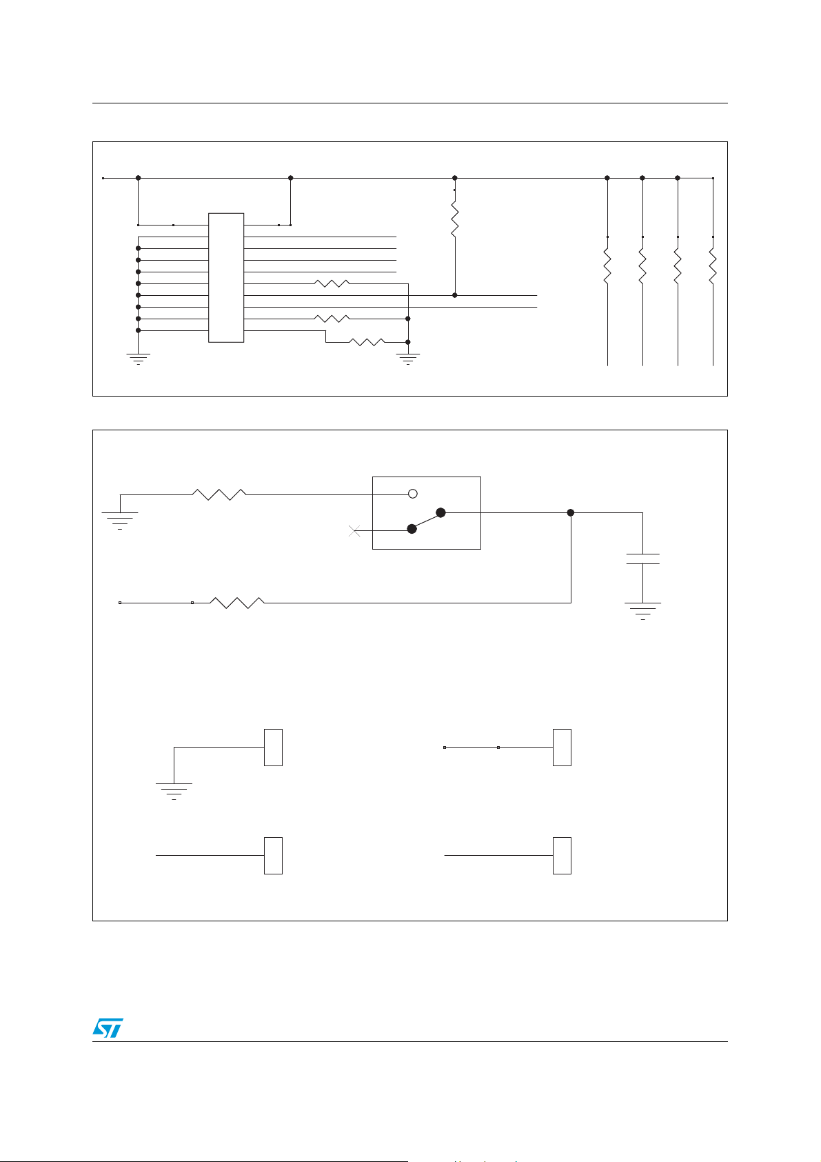
Figure 2. JTAG interface
Figure 3. Mode selection switch
Doc ID 022310 Rev 2 3/8

Schematics STEVAL-PCC009V4
5V0
USBDP
USBDM
GND
5V0 USBDM
PC4
GND
3V3
3V3
3V3
USBDP PD2
3V3
U2
USBLC6-2P6
U2
USBLC6-2P6
I/O2
4
VBUS
5
I/O1
6
I/O11GND2I/O2
3
R221MR22
1M
R21
1k5
R21
1k5
D2
POWERD2POWER
J2
USB_MINIB TYPEJ2USB_MINIB TYPE
USB_VCC
1
USBDM
2
USBDP
3
USB_GND
5
SHELL6SHELL7SHELL
8
ID
4
SHELL
9
C43
10uF
C43
10uF
C42
4.7nF
C42
4.7nF
C40
4.7uF
C40
4.7uF
C44
100nF
C44
100nF
U3
LD1117D33TRU3LD1117D33TR
VIN
4
NC
5
VOUT
6
GND1VOUT2VOUT
3
VOUT
7
NC
8
C41
100nF
C41
100nF
R23
360
R23
360
AM10184v1
Figure 4. Power supply
4/8 Doc ID 022310 Rev 2

STEVAL-PCC009V4 Schematics
3V3
3V3
GND
GND
VDD_T
GND_T
VDD_T
GND_T
PB9_TIM4_CH4
PB8_TIM4_CH3
PB8_TIM4_CH3_DB
3V3
GND
VDD_T
GND_T
PA2_USART2_TX
PA2_USART2_TX_DB
PA3_USART2_RX
VDD_T
GND_T
3V3
GND
PA3_USART2_RX_DB
3V3
GND
VDD_T
GND_T
PA7_SPI1_MOSI
PA7_SPI1_MOSI_DB
PA1_USART2_RTS
VDD_T
GND_T
3V3
GND
PA1_USART2_RTS_DB
3V3
GND
VDD_T
GND_T
PA0_USART2_CTS
PA0_USART2_CTS_DB
3V3
GND
VDD_T
GND_T
PA4_USART2_CLK
PA4_USART2_CLK_DB
3V3
GND
VDD_T
GND_T
PA5_SPI1_SCK
PA5_SPI1_SCK_DB
VDD_T
PA6_SPI1_MISO
GND_T
PA6_SPI1_MISO_DB
GND
3V3
VDD_T
PC0_GPIO_IN10
GND_T
PC0_GPIO_IN10_DB
GND
3V3
3V3
GND
VDD_T
GND_T
GND
3V3 VDD_T
GND_T
GND
GND_T
3V3
VDD_T
PB5_I2C1_SMBAI
VDD_T
GND_T
3V3
GND
PB5_I2C1_SMBAI_DB
PB7_I2C1_SDA
PB6_I2C1_SCL
PB7_I2C1_SDA_DB
PB6_I2C1_SCL_DB
PB9_TIM4_CH4_DB
R35
47E
R35
47E
C22
100nF
C22
100nF
C19
100nF
C19
100nF
C13
DNM
C13
DNM
R13
10k
R13
10k
R34
47E
R34
47E
R25
47E
R25
47E
U12
ACPL-072L
U12
ACPL-072L
VDD1
1
NC
3
GND2
5
NC
7
Vi
2
GND1
4
Vo
6
VDD2
8
C35
100nF
C35
100nF
R32
47E
R32
47E
C11
DNM
C11
DNM
C24
100nF
C24
100nF
C33
100nF
C33
100nF
R26
47E
R26
47E
U6
ACPL-072LU6ACPL-072L
VDD1
1
NC
3
GND2
5
NC
7
Vi
2
GND1
4
Vo
6
VDD2
8
C20
100nF
C20
100nF
C31
100nF
C31
100nF
C10
DNM
C10
DNM
U13
ACPL-072L
U13
ACPL-072L
VDD1
1
NC
3
GND2
5
NC
7
Vi
2
GND1
4
Vo
6
VDD2
8
C30
100nF
C30
100nF
U16
ADUM1250SRZ
U16
ADUM1250SRZ
VDD1
1
NC
3
GND2
5
NC
7
Vi
2
GND1
4
Vo
6
VDD2
8
C17
100nF
C17
100nF
R30
47E
R30
47E
C37
100nF
C37
100nF
C14
100nF
C14
100nF
C23
100nF
C23
100nF
C27
100nF
C27
100nF
U10
ACPL-072L
U10
ACPL-072L
VDD1
1
NC
3
GND2
5
NC
7
Vi
2
GND1
4
Vo
6
VDD2
8
U9
ACPL-072LU9ACPL-072L
VDD1
1
NC
3
GND2
5
NC
7
Vi
2
GND1
4
Vo
6
VDD2
8
U15
ACPL-072L
U15
ACPL-072L
VDD1
1
NC
3
GND2
5
NC
7
Vi
2
GND1
4
Vo
6
VDD2
8
R31
47E
R31
47E
C18
100nF
C18
100nF
U5
ACPL-072LU5ACPL-072L
VDD1
1
NC
3
GND2
5
NC
7
Vi
2
GND1
4
Vo
6
VDD2
8
R28
47E
R28
47E
U8
ACPL-072LU8ACPL-072L
VDD1
1
NC
3
GND2
5
NC
7
Vi
2
GND1
4
Vo
6
VDD2
8
C45
100nF
C45
100nF
C26
100nF
C26
100nF
U11
ACPL-072L
U11
ACPL-072L
VDD1
1
NC
3
GND2
5
NC
7
Vi
2
GND1
4
Vo
6
VDD2
8
R29
47E
R29
47E
R11
10k
R11
10k
U14
ACPL-072L
U14
ACPL-072L
VDD1
1
NC
3
GND2
5
NC
7
Vi
2
GND1
4
Vo
6
VDD2
8
C21
100nF
C21
100nF
C36
100nF
C36
100nF
C32
100nF
C32
100nF
R33
47E
R33
47E
U4
ACPL-072LU4ACPL-072L
VDD1
1
NC
3
GND2
5
NC
7
Vi
2
GND1
4
Vo
6
VDD2
8
R27
47E
R27
47E
C34
100nF
C34
100nF
R12
10k
R12
10k
R24
47E
R24
47E
C46
100nF
C46
100nF
C29
100nF
C29
100nF
C16
100nF
C16
100nF
C38
100nF
C38
100nF
C28
100nF
C28
100nF
C15
100nF
C15
100nF
U7
ACPL-072LU7ACPL-072L
VDD1
1
NC
3
GND2
5
NC
7
Vi
2
GND1
4
Vo
6
VDD2
8
C12
DNM
C12
DNM
R14
10k
R14
10k
AM10185v1
Figure 5. Opto-isolator section
Doc ID 022310 Rev 2 5/8

Schematics STEVAL-PCC009V4
PA1_USART2_RTS_DBPA0_USART2_CTS_DB
PA2_USART2_TX_DB PA3_USART2_RX_DB
PB9_TIM4_CH4_DB
PB8_TIM4_CH3_DB
PA4_USART2_CLK_DB
PB6_I2C1_SCL_DB
PA6_SPI1_MISO_DB
PA5_SPI1_SCK_DB
PA7_SPI1_MOSI_DB
PC0_GPIO_IN10_DB
PB7_I2C1_SDA_DB
PB5_I2C1_SMBAI_DB
GND_TVDD_T
C39
100nF
C39
100nF
J3
CON16A
J3
CON16A
1 2
3 4
5 6
7 8
9 10
11 12
13 14
15 16
AM10186V1
Figure 6. 16-pin communication interface
6/8 Doc ID 022310 Rev 2

STEVAL-PCC009V4 Revision history
2 Revision history
Table 1. Document revision history
Date Revision Changes
04-Oct-2011 1 Initial release.
16-Jul-2012 2
Updated cover page.
Minor text changes.
Doc ID 022310 Rev 2 7/8

STEVAL-PCC009V4
Please Read Carefully:
Information in this document is provided solely in connection with ST products. STMicroelectronics NV and its subsidiaries (“ST”) reserve the
right to make changes, corrections, modifications or improvements, to this document, and the products and services described herein at any
time, without notice.
All ST products are sold pursuant to ST’s terms and conditions of sale.
Purchasers are solely responsible for the choice, selection and use of the ST products and services described herein, and ST assumes no
liability whatsoever relating to the choice, selection or use of the ST products and services described herein.
No license, express or implied, by estoppel or otherwise, to any intellectual property rights is granted under this document. If any part of this
document refers to any third party products or services it shall not be deemed a license grant by ST for the use of such third party products
or services, or any intellectual property contained therein or considered as a warranty covering the use in any manner whatsoever of such
third party products or services or any intellectual property contained therein.
UNLESS OTHERWISE SET FORTH IN ST’S TERMS AND CONDITIONS OF SALE ST DISCLAIMS ANY EXPRESS OR IMPLIED
WARRANTY WITH RESPECT TO THE USE AND/OR SALE OF ST PRODUCTS INCLUDING WITHOUT LIMITATION IMPLIED
WARRANTIES OF MERCHANTABILITY, FITNESS FOR A PARTICULAR PURPOSE (AND THEIR EQUIVALENTS UNDER THE LAWS
OF ANY JURISDICTION), OR INFRINGEMENT OF ANY PATENT, COPYRIGHT OR OTHER INTELLECTUAL PROPERTY RIGHT.
UNLESS EXPRESSLY APPROVED IN WRITING BY TWO AUTHORIZED ST REPRESENTATIVES, ST PRODUCTS ARE NOT
RECOMMENDED, AUTHORIZED OR WARRANTED FOR USE IN MILITARY, AIR CRAFT, SPACE, LIFE SAVING, OR LIFE SUSTAINING
APPLICATIONS, NOR IN PRODUCTS OR SYSTEMS WHERE FAILURE OR MALFUNCTION MAY RESULT IN PERSONAL INJURY,
DEATH, OR SEVERE PROPERTY OR ENVIRONMENTAL DAMAGE. ST PRODUCTS WHICH ARE NOT SPECIFIED AS "AUTOMOTIVE
GRADE" MAY ONLY BE USED IN AUTOMOTIVE APPLICATIONS AT USER’S OWN RISK.
Resale of ST products with provisions different from the statements and/or technical features set forth in this document shall immediately void
any warranty granted by ST for the ST product or service described herein and shall not create or extend in any manner whatsoever, any
liability of ST.
ST and the ST logo are trademarks or registered trademarks of ST in various countries.
Information in this document supersedes and replaces all information previously supplied.
The ST logo is a registered trademark of STMicroelectronics. All other names are the property of their respective owners.
© 2012 STMicroelectronics - All rights reserved
STMicroelectronics group of companies
Australia - Belgium - Brazil - Canada - China - Czech Republic - Finland - France - Germany - Hong Kong - India - Israel - Italy - Japan -
Malaysia - Malta - Morocco - Philippines - Singapore - Spain - Sweden - Switzerland - United Kingdom - United States of America
www.st.com
8/8 Doc ID 022310 Rev 2
 Loading...