

S-Touch® product family interface demonstration board
Features
■ Generic interface for various S-Touch
family demonstration boards
■ DFU capability for reprogramming
■ 10-pin interface for serial communication
■ USB powered
■ RoHS compliant
Description
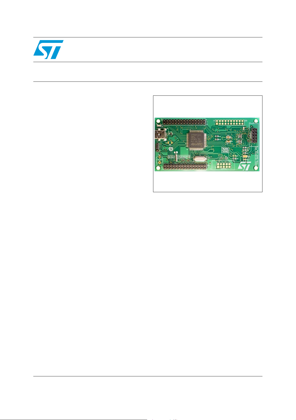
The STEVAL-PCC009V3 is a demonstration
motherboard based on the STM32
microcontroller, used as the generic interface for
various S-Touch
daughterboards (e.g. STEVAL-ICB002V1 based
on the STMPE821).
®
product family demonstration
®
product
STEVAL-PCC009V3
based on the STM32
Data brief
STEVAL-PCC009V3
Power to the STEVAL-PCC009V3 is provided by a
USB mini B-type connector, while power to the
capacitive touch daughterboards is supplied by
the STEVAL-PCC009V3 via the 10-pin connector.
The STEVAL-PCC009V3 is also able to work in
DFU mode to reprogram the STM32
microcontroller.
September 2011 Doc ID 022231 Rev 1 1/7
For further information contact your local STMicroelectronics sales office.
www.st.com
7
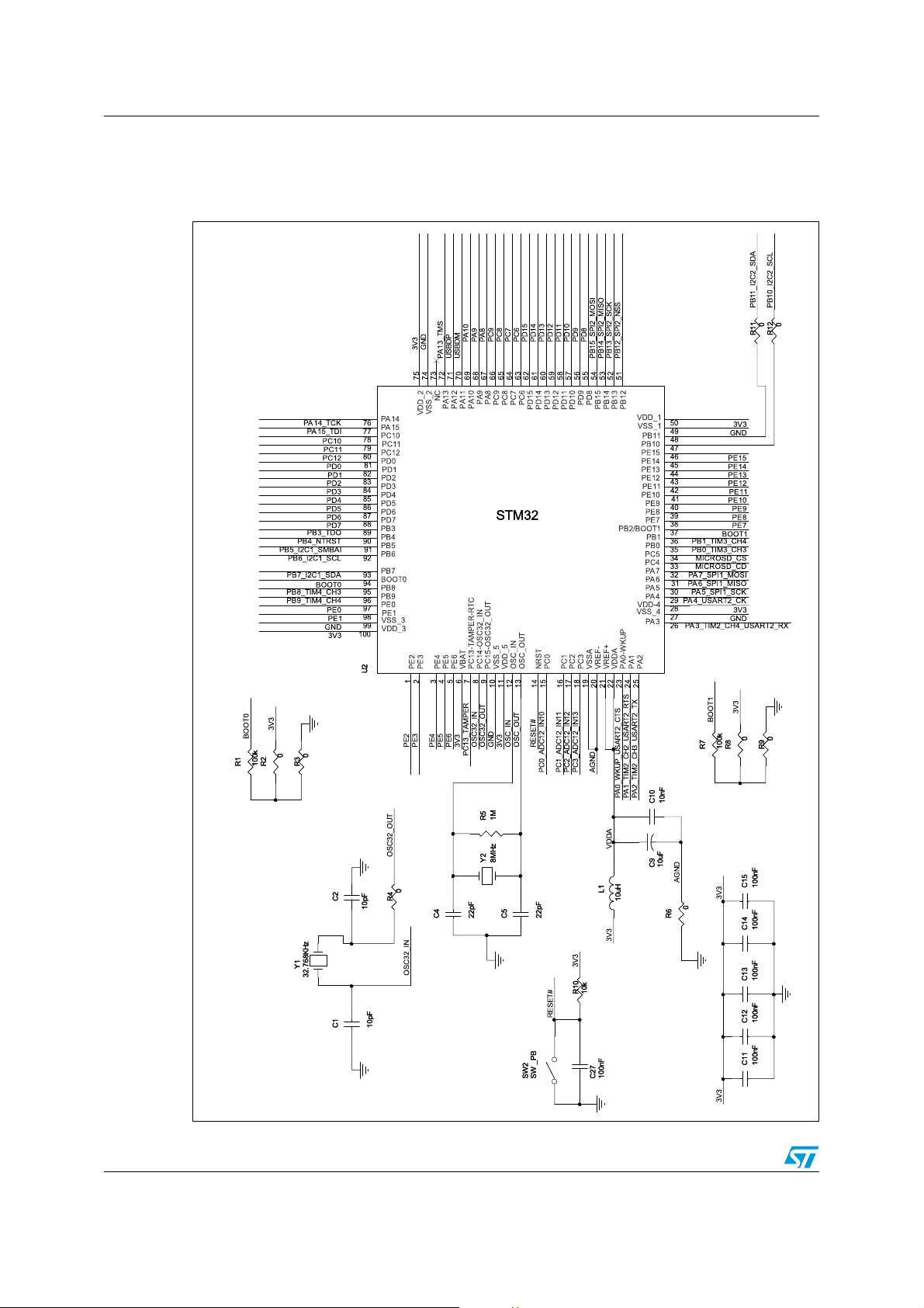
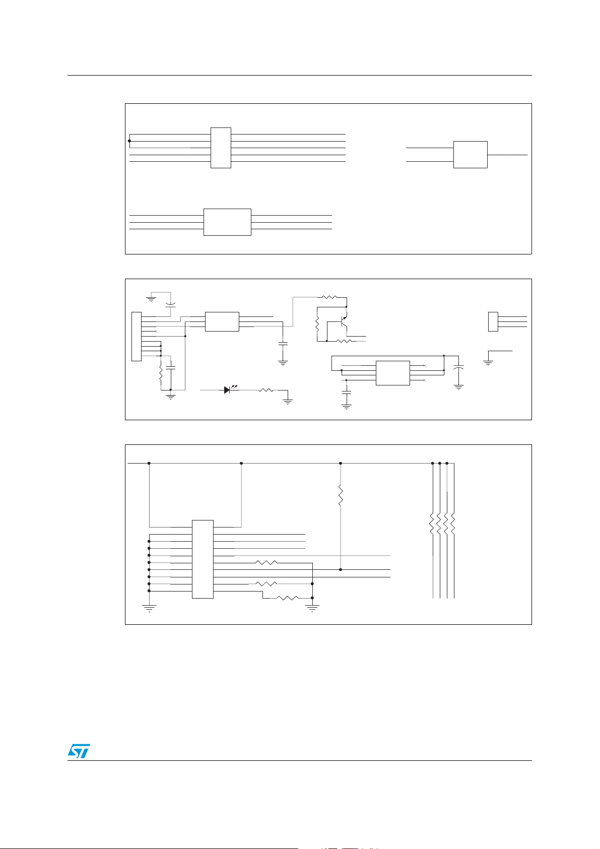
Schematic diagrams STEVAL-PCC009V3
1 Schematic diagrams
Figure 1. Microcontroller
2/7 Doc ID 022231 Rev 1
AM10138V1
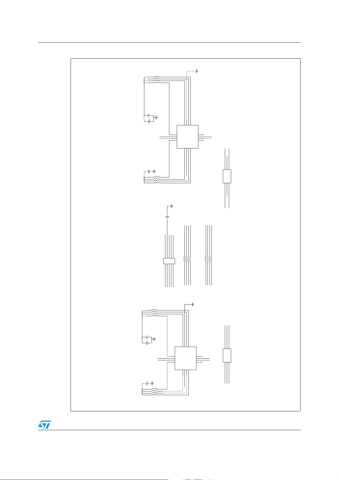
STEVAL-PCC009V3 Schematic diagrams
Figure 2. Synchronous interface
EXB-38V472JV
EXB-38V472JV
RN6
RN6
1
8
2
7
3
6
5
4
V_CON
C19
C19
1uF
1uF
C18
0.1uF
C18
0.1uF
C17
C17
3V3
1
2
3
4
PB14_SPI2_MISO_DB
V_CON
3V3
0.1uF
0.1uF
PB14_SPI2_MISO
8
7
6
5
RN5
RN5
EXB-38V472JV
EXB-38V472JV
PB15_SPI2_MOSI_DB
PB13_SPI2_SCK_DB
PB12_SPI2_NSS_DB
10
12
11
GND
I/OVCC49I/OVCC3
I/OVCC2
NC
I/OVCC1
13
VCC
14
VL
15
I/OVL1
16
U10
U10
8
VCC
V_CON
7
VL
3V3
6
NC
5
ST2349
OE2I/OVL3
I/OVL2
3
4
1
3V3
PB12_SPI2_NSS
PB13_SPI2_SCK
PB15_SPI2_MOSI
ST2349
I/OVL4
GND
PB13_SPI2_SCK_DB
PB12_SPI2_NSS_DB
6
5
6
445
3
1
2
ESDALC6V1M6U8ESDALC6V1M6
U8
1
3
2
GND
PB14_SPI2_MISO_DB
PB15_SPI2_MOSI_DB
C3
100nFC3100nF
PB15_SPI2_MOSI_DB
PB10_I2C2_SCL_DB
PB14_SPI2_MISO_DB
I/OVCC1
VCC
VL
I/OVL1
U5
PB0_TIM3_CH3_DB
876
5
RN1
RN1
123
4
SPI_CON10AJ2SPI_CON10A
PB10_I2C2_SCL
PB14_SPI2_MISO
PB0_TIM3_CH3
PB15_SPI2_MOSI
PB0_TIM3_CH3_DB
PB1_TIM3_CH4_DB
PB11_I2C2_SDA_DB
11
10
12
9
GND
I/OVCC4
I/OVCC3
I/OVCC2
VCC
I/OVL21OE2I/OVL33I/OVL4
4
3V3
PB11_I2C2_SDA
PB0_TIM3_CH3
PB1_TIM3_CH4
V_CON
PB1_TIM3_CH4_DB
PB12_SPI2_NSS_DB
PB13_SPI2_SCK_DB
PB11_I2C2_SDA_DB
J2
5 6
9 10
1 2
3 4
7 8
GND
PB14_SPI2_MISO_ DB
PB10_I2C2_SCL_DB
PB15_SPI2_MOSI_ DB
PB0_TIM3_CH3_DB
RN4
RN4
EXB-38V472JV
EXB-38V472JV
1
8
2
7
3
6
4
5
C8
1uFC81uF
C7
0.1uFC70.1uF
C6
3V3 V_CON
1
2
3
4
PB10_I2C2_SCl_DB
13
14
15
16
0.1uFC60.1uF
PB10_I2C2_SCL
8
7
6
5
RN3
RN3
EXB-38V472JV
EXB-38V472JV
PB12_SPI2_NSS_DB
PB11_I2C2_SDA_DB
PB13_SPI2_SCK_DB
PB1_TIM3_CH4_DB
876
5
RN2
RN2
EXB-38V472JV
EXB-38V472JV
EXB-38V472JV
NC
8
7
VL
6
NC
5
ST2349U5ST2349
EXB-38V472JV
123
4
PB11_I2C2_SDA
PB1_TIM3_CH4
PB13_SPI2_SCK
PB12_SPI2_NSS
GNDGND
PB11_I2C2_SDA_DB
PB1_TIM3_CH4_DB
6
44556
V_CONV_CON
3V33V3
11223
ESDALC6V1M6U4ESDALC6V1M6
U4
3
PB10_I2C2_SCL_DB
PB0_TIM3_CH3_DB
AM10139V1
Doc ID 022231 Rev 1 3/7
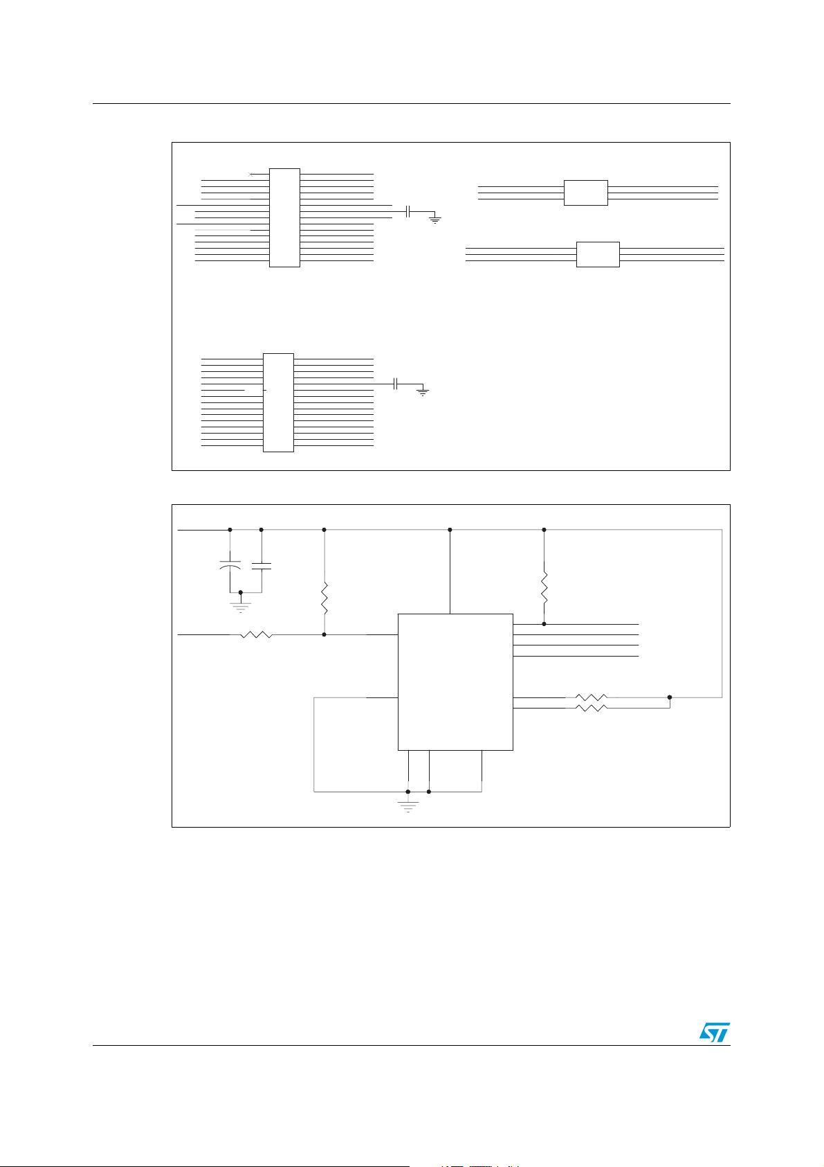
Schematic diagrams STEVAL-PCC009V3
Figure 3. Extension board interface
J4
PB6_I2C1_SCL
PB5_I2C1_SMBAI
PB8_TIM4_CH3
GND
PA2_TIM2_CH3_USAR T 2_TX
GND
PA4_USART2_CK
PA1_TIM2_CH2_USAR T 2_R T S
PE1
PE3
PE8
PE10
PE12
PE14
PD8
PD10
PD12
PD14
GND
PC6
PC8
GND
PA9
PC10
PC12
PD0
PD2
PD4
PD6
J4
1 2
3 4
5 6
7
9
11
13 14
15 16
17
19 20
21
23
25
27 28
29 30
GENERIC_30PIN
GENERIC_30PIN
J7
J7
1 2
3 4
5 6
7 8
9
11 12
13 14
15 16
17
19 20
21 22
23 24
25 26
27 28
29 30
GENERIC_30PIN
GENERIC_30PIN
GND
PB7_I2C1_SDA
GND
PB9_TIM4_CH4
8
GND
10
PA3_TIM2_CH4_USAR T 2_R X
12
V_CON
PA0_WKUP_USART2_CTS
PE0
18
PE2
PE4
22
PE9
24
PE11
26
PE13
PE15
PD9
PD11
PD13
PD15
V_CON
10
PC7
PC9
PA8
PA10
18
PC11
PC13_TAMPER
PD1
PD3
PD5
PD7
C26
C26
100nF
100nF
C16
C16
100nF
100nF
U6
PA2_TIM2_CH3_USART2_TX
GND GND
PA4_USART2_CK
PA0_WKUP_USART2_CTS
GND GND
PE1
U6
1
1
2
2
3
3
ESDALC6V1M6
ESDALC6V1M6
1
2
3
U7
U7
1
2
3
ESDALC6V1M6
ESDALC6V1M6
6
6
5
5
4
4
6
6
5
5
4
4
PA3_TIM2_CH4_USART2_RX
PE0
PA1_TIM2_CH2_USART2_RTS
PE2
AM10140V1
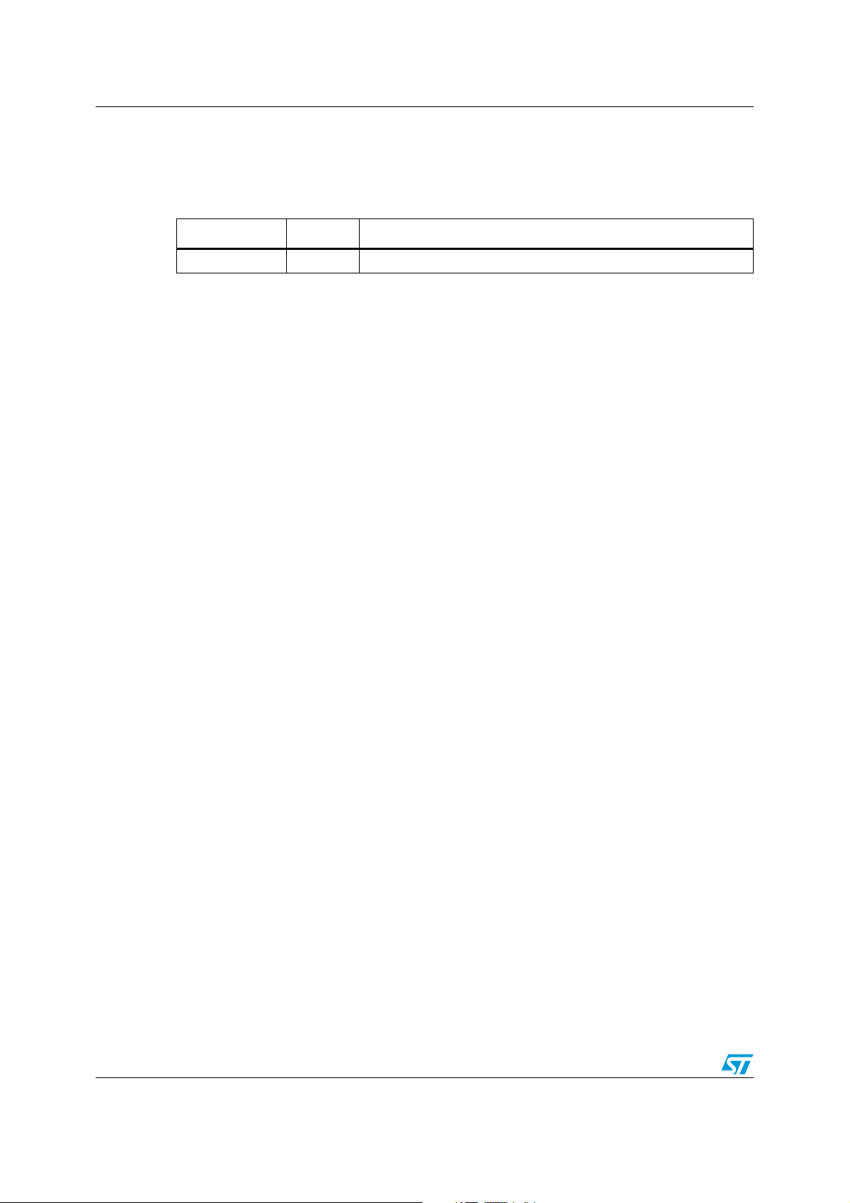
Figure 4. MicroSD
3V3
C25
R22
R22
500
500
C25
100nF
100nF
C24
C24
4.7uF
4.7uF
MICRO SD_CD
R20
R20
100k
100k
10
R21
R21
(DNM)
(DNM)
4
J8
J8
9
CD
COM
VSS
VSS
11
12
VDD
DATA_IN
SCLK
DATA_OUT
RSV
RSV
VSS2
6
CS
MMC_CON
MMC_CON
2
3
5
7
8
1
MICRO SD_CS
PA7_SPI1_M OSI
PA5_SPI1_SCK
PA6_SPI1_MISO
R24
R24
R23
R23
100k
100k
100k
100k
AM10141V1
4/7 Doc ID 022231 Rev 1
STEVAL-PCC009V3 Schematic diagrams
Figure 5. Analog interface
J1
J1
AGND
AGND
PE5
VDDA
PC0_ADC12_IN 10 PC3_ADC12_IN 13
AGND
PC1_ADC12_IN 11
1
3 4
5
7 8
9 10
ANALOG_CONN
ANALOG_CONN
U3
U3
1
1
2
2
3
3
ESDALC6V1M6
ESDALC6V1M6
2
6
6
5
4
PC0_ADC12_IN 10
PC1_ADC12_IN 11
PC2_ADC12_IN 12
PE6
PC3_ADC12_IN 13
6
AGND
5
PC2_ADC12_IN 12
4
PE5
PE6
U1
U1
1
1
2
2
ESDALC6V1M3
ESDALC6V1M3
AGND
3
3
AM10142V1
Figure 6. Power supply
R18
R18
1k5
1k5
R26
R26
1k5
1k5
Q1
2STR1215Q12STR1215
3V3
PE7
R27
R27
1k5
1k5
GND
3V3 3V3
5V0
C22
C22
100nF
100nF
U11
U11
1
GND
2
VOUT
3
VOUT
VIN4NC
LD1117D33TR
LD1117D33TR
VOUT
VOUT
3V3
8
NC
7
6
5
C21
C21
10uF
10uF
CON3J6CON3
J6
GND
3V3
1
V_CON
2
5V0
3
AM10143V1
CON9J5CON9
J5
1
2
3
4
5
6
7
8
9
C28
C28
U9
U9
4.7uF
4.7uF
5V0 USBDM
R191MR19
1M
C23
C23
4.7nF
4.7nF
1
2
3
3V3
1
2
3
USBLC6-2P6
USBLC6-2P6
D1
POWERD1POWER
6
6
3V3
5
5
USBDP
4
4
C20
C20
4.7nF
4.7nF
R25
R25
500
500
Figure 7. JTAG interface
3V33V3
R14
R14
10k
10k
J3
J3
12
34
56
78
910
1112
1314
16
JTAG_20PIN
JTAG_20PIN
15
1718
1920
PB4_NTRST
PA15_TDI
PA13_TMS
PA14_TCK
R15
R15
10k
10k
R16
R16
10k
10k
R17
R17
10k
10k
PB3_TDO
RESET#
3V3
876
123
PB4_NTR ST
PA15_TDI
5
RN7
RN7
RESAR_IS_4/SM_10K
RESAR_IS_4/SM_10K
4
PA13_TMS
PA14_TCK
AM10144V1
Doc ID 022231 Rev 1 5/7
Revision history STEVAL-PCC009V3
2 Revision history
Table 1. Document revision history
Date Revision Changes
15-Sep-2011 1 Initial release.
6/7 Doc ID 022231 Rev 1

STEVAL-PCC009V3
Please Read Carefully:
Information in this document is provided solely in connection with ST products. STMicroelectronics NV and its subsidiaries (“ST”) reserve the
right to make changes, corrections, modifications or improvements, to this document, and the products and services described herein at any
time, without notice.
All ST products are sold pursuant to ST’s terms and conditions of sale.
Purchasers are solely responsible for the choice, selection and use of the ST products and services described herein, and ST assumes no
liability whatsoever relating to the choice, selection or use of the ST products and services described herein.
No license, express or implied, by estoppel or otherwise, to any intellectual property rights is granted under this document. If any part of this
document refers to any third party products or services it shall not be deemed a license grant by ST for the use of such third party products
or services, or any intellectual property contained therein or considered as a warranty covering the use in any manner whatsoever of such
third party products or services or any intellectual property contained therein.
UNLESS OTHERWISE SET FORTH IN ST’S TERMS AND CONDITIONS OF SALE ST DISCLAIMS ANY EXPRESS OR IMPLIED
WARRANTY WITH RESPECT TO THE USE AND/OR SALE OF ST PRODUCTS INCLUDING WITHOUT LIMITATION IMPLIED
WARRANTIES OF MERCHANTABILITY, FITNESS FOR A PARTICULAR PURPOSE (AND THEIR EQUIVALENTS UNDER THE LAWS
OF ANY JURISDICTION), OR INFRINGEMENT OF ANY PATENT, COPYRIGHT OR OTHER INTELLECTUAL PROPERTY RIGHT.
UNLESS EXPRESSLY APPROVED IN WRITING BY TWO AUTHORIZED ST REPRESENTATIVES, ST PRODUCTS ARE NOT
RECOMMENDED, AUTHORIZED OR WARRANTED FOR USE IN MILITARY, AIR CRAFT, SPACE, LIFE SAVING, OR LIFE SUSTAINING
APPLICATIONS, NOR IN PRODUCTS OR SYSTEMS WHERE FAILURE OR MALFUNCTION MAY RESULT IN PERSONAL INJURY,
DEATH, OR SEVERE PROPERTY OR ENVIRONMENTAL DAMAGE. ST PRODUCTS WHICH ARE NOT SPECIFIED AS "AUTOMOTIVE
GRADE" MAY ONLY BE USED IN AUTOMOTIVE APPLICATIONS AT USER’S OWN RISK.
Resale of ST products with provisions different from the statements and/or technical features set forth in this document shall immediately void
any warranty granted by ST for the ST product or service described herein and shall not create or extend in any manner whatsoever, any
liability of ST.
ST and the ST logo are trademarks or registered trademarks of ST in various countries.
Information in this document supersedes and replaces all information previously supplied.
The ST logo is a registered trademark of STMicroelectronics. All other names are the property of their respective owners.
© 2011 STMicroelectronics - All rights reserved
Australia - Belgium - Brazil - Canada - China - Czech Republic - Finland - France - Germany - Hong Kong - India - Israel - Italy - Japan -
STMicroelectronics group of companies
Malaysia - Malta - Morocco - Philippines - Singapore - Spain - Sweden - Switzerland - United Kingdom - United States of America
www.st.com
Doc ID 022231 Rev 1 7/7
 Loading...