

现货库存、技术资料、百科信息、热点资讯,精彩尽在鼎好!
1
2
3
4
8
6
5
7
V
CC
V
CC
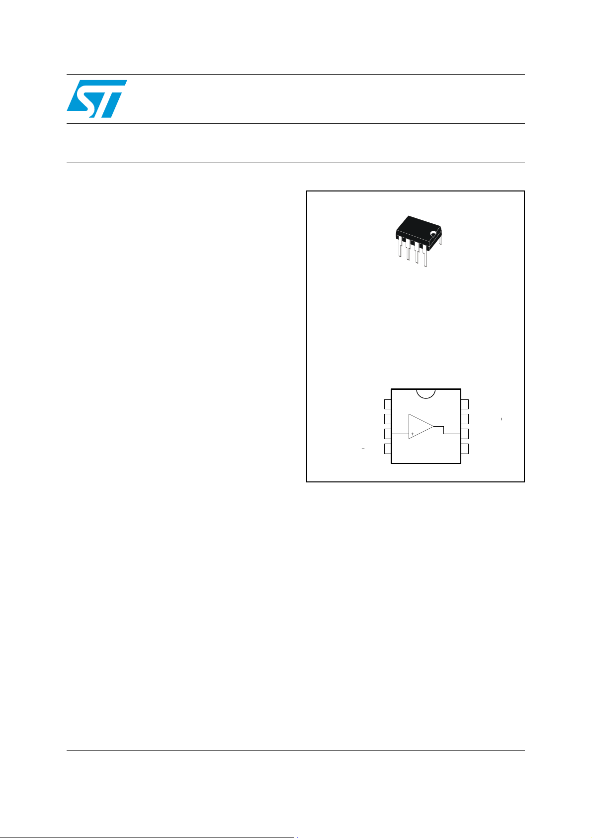
Inverting Input
Non-inverting Input Output
Offset Null 2Offset Null 1
N.C.
Very low offset single bipolar operational amplifier
Features
■ Extremely low offset: 150µV/ max.
■ Low input bias current: 1.8nA
■ LOW V
■ Ultra stable with time: 2µV/month max.
■ Wide supply voltage range: ±3V to ± 22V
■ Temperature range: 0°C to -105°C
drift: 0.5µV/°C
io
OP07
N
DIP8
(Plastic package)
Description
The OP07 is a very high precision op-amp with an
offset voltage maximu m of 150µV.
Offering also low input current (1.8nA) and high
gain (400V/mV), the OP07C is particularly
suitable for instrumentation applications .
Pin connections
(top view)
July 2007 Rev 2 1/8
www.st.com
8
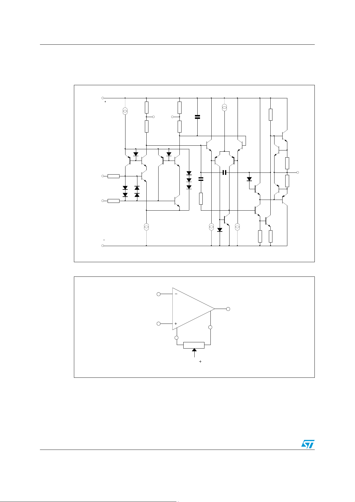
Schematic diagram OP07
Offset Null 2
Offset Null 1
20k
Ω
V
CC
1 Schematic diagram
Figure 1. Schematic diagram
V
Non-inverting
input
Inverting
input
CC
R3
D1
D2 D3
R4
R2A
Offset
Null
R1A
N2 N4
T5
T6 T4T3
T1
D4
R2B
C1
R1B
T10
D9D8
T7T9T8
D7
D6
D5
T2
C3
R5
C2
D11
T11
R7
T15
T18
R9
Output
R10
T12 T17
T16
T13
T14
V
CC
Figure 2. Input offset voltage nulling circuit
D10
R6 R8
2/8
OP07 Absolute maximum ratings
2 Absolute maximum ratings
Table 1. Absolute maximum ratings
Symbol Parameter Value Unit
V
CC
V
id
V
i
T
oper
T
stg
R
thja
R
thjc
ESD
1. Short-circuits can cause excessive heating and destructive dissipation.
are typical values.
2. R
th
3. Human body model: 100pF discharged through a 1.5kΩ resistor between two pins of the device, done for
all couples of pin combinations with other pins floating.
4. Machine model: a 200pF cap is charged to the specified voltage, then discharged directly between two pins
of the device with no external series resistor (internal resistor < 5Ω). Done for all couples of pin
combinations with other pins floating.
5. Charged device model: all pins plus package are charged together to the specified voltage and then
discharged directly to the ground.
Supply voltage ± 22 V
Differential input voltage ± 30 V
Input voltage ± 22 V
Operating temperature -40 to 105 °C
Storage temperature -65 to 150 °C
Thermal resistance junction to ambient
DIP8
Thermal resistance junction to case
DIP8
HBM: human body model
MM: machine model
CDM: charged device model
(3)
(4)
(5)
(1) (2)
85 °C/W
(1) (2)
41 °C/W
1.5 kV
200 V
1.5 kV
3/8

Electrical characteristics OP07
3 Electrical characteristics
Table 2. V
+
CC
= 15 V, V
-
= Ground, T
CC
= 25° C (unless otherwise specified)
amb
Symbol Parameter Min. Typ. Max. Unit
V
io
DV
I
io
DI
DI
R
R
id
R
ic
V
icm
CMR
SVR
Input offset voltage
0°C ≤ T
Long term input offset - voltage stability
Input offset voltage drift 0.5 1.8 µV/°C
io
≤ +105°C
amb
(1)
Input offset current (Vic = 0V)
0°C ≤ T
Input offset current drift 15 50 pA/°C
io
Input bias current drift 15 50 pA/°C
ib
Open loop output resistance 60 Ω
o
≤ +105°C
amb
Differential input resistance 33 MW
Common mode input resistance 120 GW
Input common mode voltage range
0°C ≤ T
Common-mode rejection ratio (V
0°C ≤ T
Supply voltage rejection ratio (V
0°C ≤ T
≤ +105°C
amb
≤ +105°C
amb
≤ +105°C
amb
ic
CC
= V
icm -min
)
= ±3 to ±18V)
±13
±13
100
97
90
86
60 150
250
0.4 2 µV/Mo
0.8 6
7
±13.5
120
104
Large signal voltage gain
= ±15, RL = 2kΩ, VO = ±10V
V
A
vd
CC
0°C ≤ T
≤ +105°C
amb
VCC = ±3, RL = 500Ω, VO = ±0.5V
120
100
100
400
400
µV
nA
V
dB
dB
V/mV
Output voltage swing
RL = 10kΩ
V
opp
SR Slew rate ( R
GBP Gain bandwidth product (R
= 2kΩ
R
L
R
= 1kΩ
L
0°C ≤ T
≤ +105°C RL = 2kΩ
amb
= 2kΩ, CL = 100pF) 0.17 V/µs
L
= 2kΩ, CL = 100pF, f = 100kHz) 0.5 MHz
L
Supply current - no load
I
CC
0°C ≤ T
≤ +105°C
amb
VCC = ±3V
4/8
±12
±11.5
±11
±13
±12.8
±12
2.7
0.67
5
6
1.3
V
mA

OP07 Package information
Table 2. V
+
= 15 V, V
CC
-
= Ground, T
CC
= 25° C (unless otherwise specified) (continued)
amb
Symbol Parameter Min. Typ. Max. Unit
Equivalent input noise voltage
e
n
f = 10Hz
f = 100Hz
f = 1kHz
11
10.5
10
20
13.5
11.5
nV
----------- -
Equivalent input noise current
i
n
f = 10Hz
f = 100Hz
f = 1kHz
1. Long term input offset voltage stability refers to the average trend line of Vio vs time over extended periods after the first 30
days of operation.
0.3
0.2
0.1
0.9
0.3
0.2
pA
----------- -
4 Package information
In order to meet environmental requirements, ST offers these devices in ECOPACK®
packages. These packages have a lead-free second level interconnect . The category of
second level interconnect is marked on the package and on the inner box label, in
compliance with JEDEC Standard JESD97. The maximum ratings related t o soldering
conditions are also marked on the inner box label. ECOPACK is an ST trademark.
ECOPACK specifications are available at: www.st.com.
Hz
Hz
5/8

Package information OP07
Figure 3. DIP8 package mechanical data
Dimensions
Ref.
Min. Typ. Max. Min. Typ. Max.
A5.330.210
A1 0.38 0.015
A2 2.92 3.30 4.95 0.115 0.130 0.195
b 0.36 0.46 0.56 0.014 0.018 0.022
b2 1.14 1.52 1.78 0.045 0.060 0.070
c 0.20 0.25 0.36 0.008 0.010 0.014
D 9.02 9.27 10.16 0.355 0.365 0.400
E 7.62 7.87 8.26 0.300 0.310 0.325
E1 6.10 6.35 7.11 0.240 0.250 0.280
e 2.54 0.100
eA 7.62 0.300
eB 10.92 0.430
L 2.92 3.30 3.81 0.115 0.130 0.150
Millimeters Inches
6/8

OP07 Ordering information
5 Ordering information
Table 3. Order codes
Part number
OP07C
OP07CN
Temperature
range
0°C, +105°C DIP8 Tube OP07CN
6 Revision history
Table 4. Document revision history
Date Revision Changes
20-May-2003 1 Initial release.
23-Jul-2007 2
Package Packing Marking
Format update.
, R
R
thja
, and ESD values added in Table 1: Absolute maximum
thjc
ratings.
Temperature range modified to 0-105°C.
7/8

OP07
Please Read Carefully:
Information in this document is provided solely in connection with ST products. STMicroelectronics NV and its subsidiaries (“ST”) reserve the
right to make changes, corrections, modifications or improvements, to this document, and the products and services described herein at any
time, without notice.
All ST products are sold pursuant to ST’s terms and conditions of sale.
Purchasers are solely res ponsibl e fo r the c hoic e, se lecti on an d use o f the S T prod ucts and s ervi ces d escr ibed he rein , and ST as sumes no
liability whatsoever relati ng to the choice, selection or use of the ST products and services described herein.
No license, express or implied, by estoppel or otherwise, to any intellectual property rights is granted under this document. If any part of this
document refers to any third pa rty p ro duc ts or se rv ices it sh all n ot be deem ed a lice ns e gr ant by ST fo r t he use of su ch thi r d party products
or services, or any intellectua l property c ontained the rein or consi dered as a warr anty coverin g the use in any manner whats oever of suc h
third party products or servi ces or any intellectual property contained therein.
UNLESS OTHERWISE SET FORTH IN ST’S TERMS AND CONDITIONS OF SALE ST DISCLAIMS ANY EXPRESS OR IMPLIED
WARRANTY WITH RESPECT TO THE USE AND/OR SALE OF ST PRODUCTS INCLUDING WITHOUT LIMITATION IMPLIED
WARRANTIES OF MERCHANTABILITY, FITNESS FOR A PARTICUL AR PURPOS E (AND THEIR EQUIVALE NTS UNDER THE LAWS
OF ANY JURISDICTION), OR INFRINGEMENT OF ANY PATENT, COPYRIGHT OR OTHER INTELLECTUAL PROPERTY RIGHT.
UNLESS EXPRESSLY APPROVED IN WRITING BY AN AUTHORIZED ST REPRESENTATIVE, ST PRODUCTS ARE NOT
RECOMMENDED, AUTHORIZED OR WARRANTED FOR USE IN MILITARY, AIR CRAFT, SPACE, LIFE SAVING, OR LIFE SUSTAINING
APPLICATIONS, NOR IN PRODUCTS OR SYSTEMS WHERE FAILURE OR MALFUNCTION MAY RESULT IN PERSONAL INJ URY,
DEATH, OR SEVERE PROPERTY OR ENVIRONMENTAL DAMAGE. ST PRODUCTS WHICH ARE NOT SPECIFIED AS "AUTOMOTIVE
GRADE" MAY ONLY BE USED IN AUTOMOTIVE APPLICATIONS AT USER’S OWN RISK.
Resale of ST products with provisions different from the statements and/or technical features set forth in this document shall immediately void
any warranty granted by ST fo r the ST pro duct or serv ice describe d herein and shall not cr eate or exten d in any manne r whatsoever , any
liability of ST.
ST and the ST logo are trademarks or registered trademarks of ST in various countries.
Information in this document su persedes and replaces all informati on previously supplied.
The ST logo is a registered trademark of STMicroelectronics. All other names are the property of their respective owners.
© 2007 STMicroelectronics - All rights reserved
STMicroelectronics group of compan ie s
Australia - Belgium - Brazil - Canada - China - Czech Republic - Finland - France - Germany - Hong Kong - India - Israel - Italy - Japan -
Malaysia - Malta - Morocco - Singapore - Spain - Sweden - Switzerland - United Kingdom - United States of America
www.st.com
8/8
 Loading...