

Features
■ Low turn-off time
■ Maximum operating frequency greater than
500 kHz
■ Timing from microseconds to hours
■ Operates in both astable and monostable
modes
■ Output can source or sink up to 200 mA
■ Adjustable duty cycle
■ TTL compatible
■ Temperature stability of 0.005% per °C
Description
NE555
SA555 - SE555
General-purpose single bipolar timers
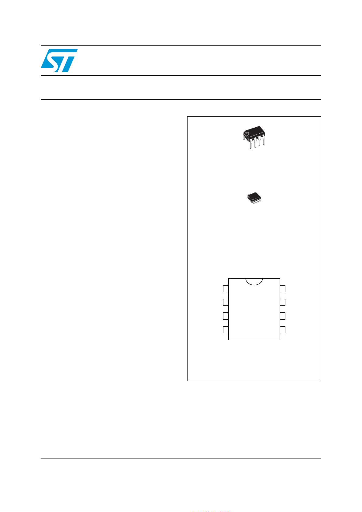
N
DIP8
(Plastic package)
D
SO8
(Plastic micropackage)
The NE555, SA555, and SE555 monolithic timing
circuits are highly stable controllers capable of
producing accurate time delays or oscillation. In
the time delay mode of operation, the time is
precisely controlled by one external resistor and
capacitor. For a stable operation as an oscillator,
the free running frequency and the duty cycle are
both accurately controlled with two external
resistors and one capacitor.
The circuit may be triggered and reset on falling
waveforms, and the output structure can source
or sink up to 200 mA.
Pin connections
(top view)
1
2
36
4
1 - GND
2 - Trigger
3 - Output
4 - Reset
8
7
5
5 - Control voltage
6 - Threshold
7 - Discharge
8 - V
CC
January 2012 Doc ID 2182 Rev 6 1/20
www.st.com
20

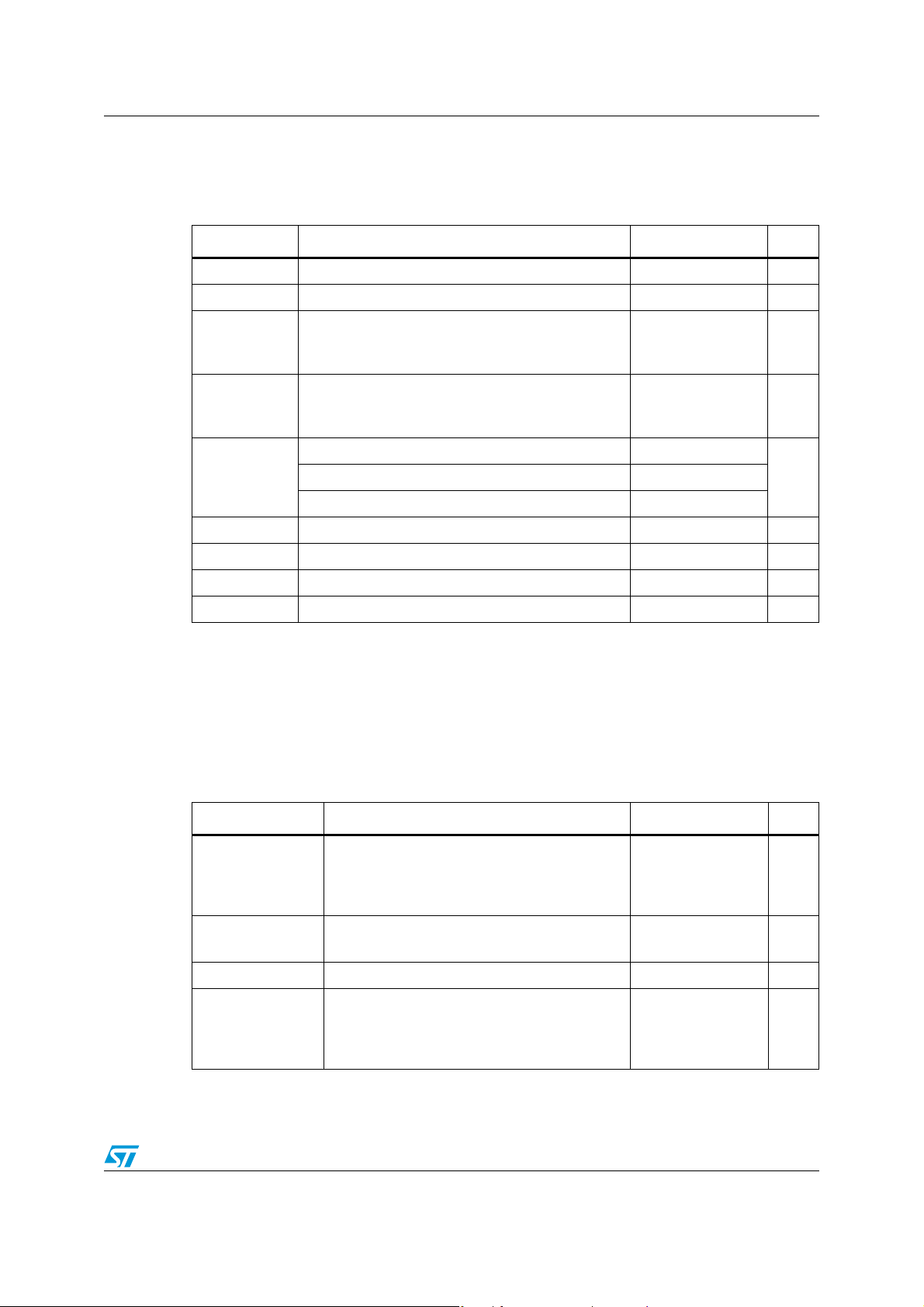
Schematic diagrams NE555 - SA555 - SE555
1 Schematic diagrams
Figure 1. Block diagram
+
V
CC
5kΩ
THRESHOLD
CONTROL VOLTAGE
TRIGGER
COMP
5kΩ
COMP
5kΩ
R
FLIP-FLOP
S
INHIBIT/
RESET
Q
DISCHARGE
OUT
RESET
Figure 2. Schematic diagram
S
2/20 Doc ID 2182 Rev 6
NE555 - SA555 - SE555 Absolute maximum ratings and operating conditions
2 Absolute maximum ratings and operating conditions
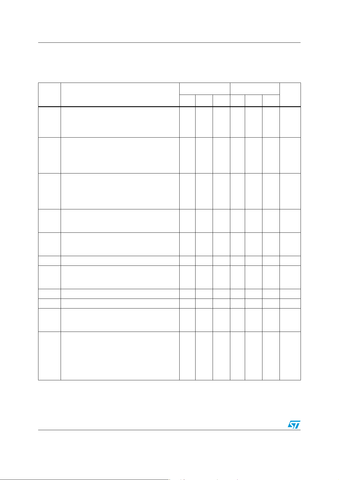
Table 1. Absolute maximum ratings
Symbol Parameter Value Unit
V
CC
I
OUT
R
thja
R
thjc
ESD
Supply voltage 18 V
Output current (sink & source) ±225 mA
(1)
(1)
85
125
41
40
1000
100
1500
°C/W
°C/W
Thermal resistance junction to ambient
DIP8
SO-8
Thermal resistance junction to case
DIP8
SO-8
Human body model (HBM)
Charged device model (CDM)
(2)
(3)
(4)
Latch-up immunity 200 mA
T
LEAD
T
j
T
stg
1. Short-circuits can cause excessive heating. These values are typical.
2. Human body model: a 100 pF capacitor is charged to the specified voltage, then discharged through a
1.5 kΩ resistor between two pins of the device. This is done for all couples of connected pin combinations
while the other pins are floating.
3. Machine model: a 200 pF capacitor is charged to the specified voltage, then discharged directly between
two pins of the device with no external series resistor (internal resistor < 5 Ω). This is done for all couples of
connected pin combinations while the other pins are floating.
4. Charged device model: all pins and the package are charged together to the specified voltage and then
discharged directly to the ground through only one pin. This is done for all pins.
Table 2. Operating conditions
Lead temperature (soldering 10 seconds) 260 °C
Junction temperature 150 °C
Storage temperature range -65 to 150 °C
VMachine model (MM)
Symbol Parameter Value Unit
Supply voltage
V
CC
NE555
SA555
SE555
, V
cl
th
, V
I
OUT
trig
reset
,
Maximum input voltage V
Output current (sink and source) ±200 mA
V
V
4.5 to 16
4.5 to 16
4.5 to 18
CC
Operating free air temperature range
T
oper
NE555
SA555
SE555
0 to 70
-40 to 105
-55 to 125
°C
Doc ID 2182 Rev 6 3/20
V
V
Electrical characteristics NE555 - SA555 - SE555
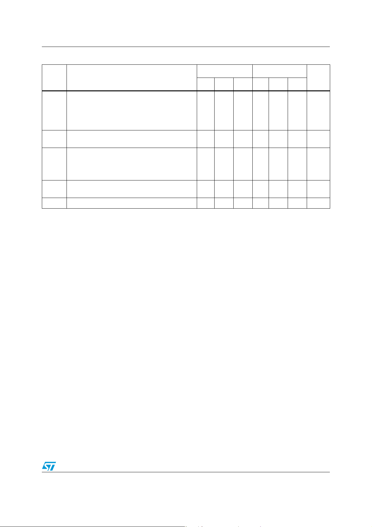
3 Electrical characteristics
Table 3. T
= +25° C, VCC = +5 V to +15 V (unless otherwise specified)
amb
Symbol Parameter
Supply current (RL = ∝)
Low state V
I
CC
High state V
= +5 V
CC
VCC = +15 V
= +5 V
CC
Timing error (monostable)
(R
= 2 kΩ to 100 kΩ, C = 0.1 μF)
A
Initial accuracy
(1)
Drift with temperature
Drift with supply voltage
Timing error (astable)
(R
R
= 1 kΩ to 100 kΩ, C = 0.1 μF, VCC= +15 V)
,
A
B
Initial accuracy
(1)
Drift with temperature
Drift with supply voltage
Control voltage level
V
CL
VCC = +15 V
= +5 V
V
CC
Threshold voltage
V
th
V
CC
= +15 V
VCC = +5 V
Threshold current
I
th
(2)
Trigger voltage
V
V
trig
I
trig
reset
VCC = +15 V
= +5 V
V
CC
Trigger current (V
Reset voltage
(3)
= 0 V) 0.5 0.9 0.5 2.0 µA
trig
Reset current
I
reset
V
V
reset
reset
= +0.4 V
= 0 V
Low level output voltage
= +15 VI
V
CC
V
OL
VCC = +5 V I
O(sink)
I
O(sink)
I
O(sink)
I
O(sink)
O(sink)
I
O(sink)
= 10 mA
= 50 mA
= 100 mA
= 200 mA
= 8 mA
= 5 mA
SE555 NE555 - SA555
Min. Typ. Max. Min. Typ. Max.
3
10
2
0.5
30
0.05
1.5
90
0.15
9.6
2.9103.33
9.4
2.7103.33
5
12
3
10
2
2
100
0.2
1
50
0.130.5
2.25
150
0.3
10.4
3.892.6103.33114
10.648.8
2.4103.33
6
15
ppm/°C
ppm/°C
11.2
4.2
0.1 0.25 0.1 0.25 µA
4.8
1.4551.67
5.2
1.9
4.5
1.151.67
5.6
2.2
0.4 0.7 1 0.4 0.7 1 V
0.1
0.4
0.1
0.4
2.5
0.1
0.05
0.4
1
0.15
0.5
2
2.2
0.1
0.4
0.1
0.4
2
0.4
1.5
0.25
0.75
2.5
2.5
0.25
0.2
0.3
0.25
0.4
0.35
Unit
mA
%
%/V
%
%/V
V
V
V
mA
V
4/20 Doc ID 2182 Rev 6
NE555 - SA555 - SE555 Electrical characteristics
Table 3. T
= +25° C, VCC = +5 V to +15 V (unless otherwise specified) (continued)
amb
SE555 NE555 - SA555
Symbol Parameter
Min. Typ. Max. Min. Typ. Max.
High level output voltage
= +15 VI
V
V
OH
CC
VCC = +5 V I
I
dis(off)
V
dis(sat)
Discharge pin leakage current
(output high) V
Discharge pin saturation voltage
(output low)
(4)
VCC = +15V, I
VCC = +5V, I
t
Output rise time
r
t
Output fall time
f
Turn off time
t
off
1. Tested at VCC = +5 V and VCC = +15 V.
2. This will determine the maximum value of R
operation and 3.5 MΩ for +5 V operation.
3. Specified with trigger input high.
4. No protection against excessive pin 7 current is necessary, providing the package dissipation rating is not exceeded.
5. Time measured from a positive pulse (from 0 V to 0.8 x V
output pin. Trigger is tied to threshold.
(5)
O(sink)
I
O(sink)
O(sink)
= 10 V
dis
= 15 mA
dis
= 4.5 mA
dis
(V
reset
= 200 mA
= 100 mA
= 100 mA
13
3
12.5
13.3
3.3
12.7
5
2.75
12.5
13.3
3.3
20 100 20 100 nA
18080480
200
100
100
200
200
18080480
200
100
100
300
300
= VCC)0.50.5µs
+ RB for 15 V operation. The maximum total (RA + RB) is 20 MΩ for +15 V
A
) on the threshold pin to the transition from high to low on the
CC
Unit
V
mV
ns
Doc ID 2182 Rev 6 5/20
Electrical characteristics NE555 - SA555 - SE555
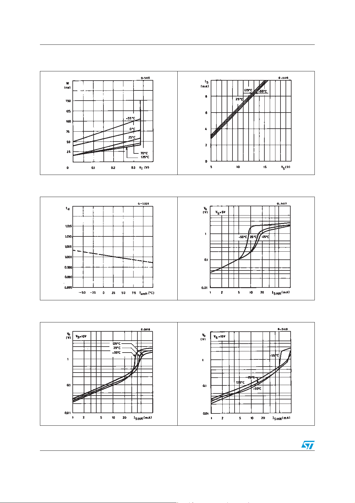
Figure 3. Minimum pulse width required for
triggering
Figure 4. Supply current versus supply
voltage
Figure 5. Delay time versus temperature Figure 6. Low output voltage versus output
sink current
Figure 7. Low output voltage versus output
Figure 8. Low output voltage versus output
sink current
6/20 Doc ID 2182 Rev 6
sink current
 Loading...