


528 Byte/264 Word Page, 1.8 V/3V, NAND Flash Memories
FEATURES SUMMARY
NAND128-A, NAND256-A
NAND512-A, NAND01G-A
128 Mbit, 256 Mbit, 512 Mbit, 1 Gbit (x8/x16)
■ HIGH DENSITY NAND FLASH MEMORIES
– Up to 1 Gbit memory array
– Up to 32 Mbit spare area
– Cost effective solutions for mass storage
applications
■ NAND INTE RFACE
– x8 or x16 bus width
– Multiplexed Address/ Data
– Pinout compatibility for all densities
■ SUPPLY VOLTAGE
– 1.8V device: V
– 3.0V device: V
■ PAGE SIZE
= 1.7 to 1.95V
DD
= 2.7 to 3.6V
DD
– x8 device: (512 + 16 spare) Bytes
– x16 device: (256 + 8 spare) Words
■ BLOCK SIZE
– x8 device: (16K + 512 spare) Bytes
– x16 device: (8K + 256 spare) Words
■ PAGE READ / PROGRAM
– Random access: 12µs (max)
– Sequential access: 50ns (min)
– Page program time: 200µs (typ)
■ COPY BACK PROGRAM MODE
– Fast page copy without external buffering
■ FAST BLOCK ERASE
– Block erase time: 2ms (Typ)
■ STATUS REGISTER
■ ELECTRONIC SIGNATURE
■ CHIP ENABLE ‘DON’T CARE’ OPTION
– Simple interface wit h microcontroller
■ SERIAL NUMBER OPTION
■ HARDWARE DATA PROTECTION
– Program/Erase locked during Power
transitions
Figure 1. Packages
TSOP48 12 x 20mm
USOP48 12 x 17 x 0.65mm
FBGA
VFBGA55 8 x 10 x 1mm
TFBGA55 8 x 10 x 1.2mm
VFBGA63 9 x 11 x 1mm
TFBGA63 9 x 11 x 1.2mm
■ DATA INTEGRITY
– 100,000 Program/Erase cycles
– 10 years Data Retention
■ RoHS COMPLIANCE
– Lead-Free Components are Compliant
with the RoHS Directive
■ DEVELOPMENT TOOLS
– Error Correction Code software and
hardware models
– Bad Blocks Management and Wear
Leveling algorithms
– File System OS Native refer ence sof tware
– Hardware simulation models
1/57February 2005

NAND128-A, NAND256-A, NAND512-A, NAND01G-A
Table 1. P r o du c t List
Reference Part Number
NAND128R3A
NAND128-A
NAND256-A
NAND512-A
NAND01G-A
NAND128W3A
NAND128R4A
NAND128W4A
NAND256R3A
NAND256W3A
NAND256R4A
NAND256W4A
NAND512R3A
NAND512W3A
NAND512R4A
NAND512W4A
NAND01GR3A
NAND01GW3A
NAND01GR4A
NAND01GW4A
2/57

NAND128-A, NAND256-A, NAND512-A, NAND01G-A
TABLE OF CONTENTS
FEATURES SUMMARY . . . . . . . . . . . . . . . . . . . . . . . . . . . . . . . . . . . . . . . . . . . . . . . . . . . . . . . . . . . . . 1
Figure 1. Packages. . . . . . . . . . . . . . . . . . . . . . . . . . . . . . . . . . . . . . . . . . . . . . . . . . . . . . . . . . . . . . 1
Table 1. Product List . . . . . . . . . . . . . . . . . . . . . . . . . . . . . . . . . . . . . . . . . . . . . . . . . . . . . . . . . . . . 2
SUMMARY DESCRIPTION. . . . . . . . . . . . . . . . . . . . . . . . . . . . . . . . . . . . . . . . . . . . . . . . . . . . . . . . . . . 7
Table 2. Product Description. . . . . . . . . . . . . . . . . . . . . . . . . . . . . . . . . . . . . . . . . . . . . . . . . . . . . . 8
Figure 2. Logic Diagram . . . . . . . . . . . . . . . . . . . . . . . . . . . . . . . . . . . . . . . . . . . . . . . . . . . . . . . . . . 8
Table 3. Signal Names . . . . . . . . . . . . . . . . . . . . . . . . . . . . . . . . . . . . . . . . . . . . . . . . . . . . . . . . . . 8
Figure 3. Logic Block Diagram . . . . . . . . . . . . . . . . . . . . . . . . . . . . . . . . . . . . . . . . . . . . . . . . . . . . . 9
Figure 4. TSOP48 and USOP48 Connections, x8 devices. . . . . . . . . . . . . . . . . . . . . . . . . . . . . . . 10
Figure 5. TSOP48 and USOP48 Connections, x16 devices. . . . . . . . . . . . . . . . . . . . . . . . . . . . . . 10
Figure 6. FBGA55 Connections, x8 devices (Top view through package) . . . . . . . . . . . . . . . . . . . 11
Figure 7. FBGA55 Connections, x16 devices (Top view through package). . . . . . . . . . . . . . . . . . 12
Figure 8. FBGA63 Connections, x8 devices (Top view through package) . . . . . . . . . . . . . . . . . . . 13
Figure 9. FBGA63 Connections, x16 devices (Top view through package). . . . . . . . . . . . . . . . . . 14
MEMORY ARRAY ORGANIZATION . . . . . . . . . . . . . . . . . . . . . . . . . . . . . . . . . . . . . . . . . . . . . . . . . . 15
Bad Blocks. . . . . . . . . . . . . . . . . . . . . . . . . . . . . . . . . . . . . . . . . . . . . . . . . . . . . . . . . . . . . . . . . . . 15
Table 4. Valid Blocks. . . . . . . . . . . . . . . . . . . . . . . . . . . . . . . . . . . . . . . . . . . . . . . . . . . . . . . . . . . 15
Figure 10.Memory Array Organization . . . . . . . . . . . . . . . . . . . . . . . . . . . . . . . . . . . . . . . . . . . . . . 15
SIGNAL DESCRIPTIONS . . . . . . . . . . . . . . . . . . . . . . . . . . . . . . . . . . . . . . . . . . . . . . . . . . . . . . . . . . . 16
Inputs/Outputs (I/O0-I/O7). . . . . . . . . . . . . . . . . . . . . . . . . . . . . . . . . . . . . . . . . . . . . . . . . . . . . . . . 16
Inputs/Outputs (I/O8-I/O15). . . . . . . . . . . . . . . . . . . . . . . . . . . . . . . . . . . . . . . . . . . . . . . . . . . . . . . 16
Address Latch Enable (AL) . . . . . . . . . . . . . . . . . . . . . . . . . . . . . . . . . . . . . . . . . . . . . . . . . . . . . . . 16
Command Latch Enable (CL) . . . . . . . . . . . . . . . . . . . . . . . . . . . . . . . . . . . . . . . . . . . . . . . . . . . . . 16
Chip Enable (E
Read Enable (R
Write Enable (W
Write Protect (WP
Ready/Busy (RB
V
Supply Voltage. . . . . . . . . . . . . . . . . . . . . . . . . . . . . . . . . . . . . . . . . . . . . . . . . . . . . . . . . . . . . 16
DD
V
Ground . . . . . . . . . . . . . . . . . . . . . . . . . . . . . . . . . . . . . . . . . . . . . . . . . . . . . . . . . . . . . . . . . . . 16
SS
). . . . . . . . . . . . . . . . . . . . . . . . . . . . . . . . . . . . . . . . . . . . . . . . . . . . . . . . . . . . . . . .16
).. . . . . . . . . . . . . . . . . . . . . . . . . . . . . . . . . . . . . . . . . . . . . . . . . . . . . . . . . . . . . . . 16
). . . . . . . . . . . . . . . . . . . . . . . . . . . . . . . . . . . . . . . . . . . . . . . . . . . . . . . . . . . . . . . 16
). . . . . . . . . . . . . . . . . . . . . . . . . . . . . . . . . . . . . . . . . . . . . . . . . . . . . . . . . . . . . . 16
). . . . . . . . . . . . . . . . . . . . . . . . . . . . . . . . . . . . . . . . . . . . . . . . . . . . . . . . . . . . . . . 16
BUS OPERATIONS. . . . . . . . . . . . . . . . . . . . . . . . . . . . . . . . . . . . . . . . . . . . . . . . . . . . . . . . . . . . . . . . 17
Command Input . . . . . . . . . . . . . . . . . . . . . . . . . . . . . . . . . . . . . . . . . . . . . . . . . . . . . . . . . . . . . . . 1 7
Address Input . . . . . . . . . . . . . . . . . . . . . . . . . . . . . . . . . . . . . . . . . . . . . . . . . . . . . . . . . . . . . . . . 17
Data Input. . . . . . . . . . . . . . . . . . . . . . . . . . . . . . . . . . . . . . . . . . . . . . . . . . . . . . . . . . . . . . . . . . . . 17
Data Output . . . . . . . . . . . . . . . . . . . . . . . . . . . . . . . . . . . . . . . . . . . . . . . . . . . . . . . . . . . . . . . . . . 17
Write Protect . . . . . . . . . . . . . . . . . . . . . . . . . . . . . . . . . . . . . . . . . . . . . . . . . . . . . . . . . . . . . . . . . 17
Standby . . . . . . . . . . . . . . . . . . . . . . . . . . . . . . . . . . . . . . . . . . . . . . . . . . . . . . . . . . . . . . . . . . . . . 17
Table 5. Bus Operations . . . . . . . . . . . . . . . . . . . . . . . . . . . . . . . . . . . . . . . . . . . . . . . . . . . . . . . . 1 7
Table 6. Address Insertion, x8 Devices. . . . . . . . . . . . . . . . . . . . . . . . . . . . . . . . . . . . . . . . . . . . . 18
3/57

NAND128-A, NAND256-A, NAND512-A, NAND01G-A
Table 7. Address Insertion, x16 Devices. . . . . . . . . . . . . . . . . . . . . . . . . . . . . . . . . . . . . . . . . . . . 18
Table 8. Address Definitions . . . . . . . . . . . . . . . . . . . . . . . . . . . . . . . . . . . . . . . . . . . . . . . . . . . . . 18
COMMAND SET . . . . . . . . . . . . . . . . . . . . . . . . . . . . . . . . . . . . . . . . . . . . . . . . . . . . . . . . . . . . . . . . . . 19
Table 9. Commands . . . . . . . . . . . . . . . . . . . . . . . . . . . . . . . . . . . . . . . . . . . . . . . . . . . . . . . . . . . 19
DEVICE OPERATIONS. . . . . . . . . . . . . . . . . . . . . . . . . . . . . . . . . . . . . . . . . . . . . . . . . . . . . . . . . . . . . 20
Pointer Operations . . . . . . . . . . . . . . . . . . . . . . . . . . . . . . . . . . . . . . . . . . . . . . . . . . . . . . . . . . . . 20
Figure 11.Pointer Operations . . . . . . . . . . . . . . . . . . . . . . . . . . . . . . . . . . . . . . . . . . . . . . . . . . . . . 20
Figure 12.Pointer Operations for Programming. . . . . . . . . . . . . . . . . . . . . . . . . . . . . . . . . . . . . . . . 21
Read Memory Array. . . . . . . . . . . . . . . . . . . . . . . . . . . . . . . . . . . . . . . . . . . . . . . . . . . . . . . . . . . . 22
Random Read . . . . . . . . . . . . . . . . . . . . . . . . . . . . . . . . . . . . . . . . . . . . . . . . . . . . . . . . . . . . . . . . . 22
Page Read. . . . . . . . . . . . . . . . . . . . . . . . . . . . . . . . . . . . . . . . . . . . . . . . . . . . . . . . . . . . . . . . . . . . 22
Sequential Row Read . . . . . . . . . . . . . . . . . . . . . . . . . . . . . . . . . . . . . . . . . . . . . . . . . . . . . . . . . . . 22
Figure 13.Read (A,B,C) Operations . . . . . . . . . . . . . . . . . . . . . . . . . . . . . . . . . . . . . . . . . . . . . . . .23
Figure 14.Read Block Diagrams . . . . . . . . . . . . . . . . . . . . . . . . . . . . . . . . . . . . . . . . . . . . . . . . . . . 23
Figure 15.Sequential Row Read Operations. . . . . . . . . . . . . . . . . . . . . . . . . . . . . . . . . . . . . . . . . . 24
Figure 16.Sequential Row Read Block Diagrams . . . . . . . . . . . . . . . . . . . . . . . . . . . . . . . . . . . . . . 24
Page Program . . . . . . . . . . . . . . . . . . . . . . . . . . . . . . . . . . . . . . . . . . . . . . . . . . . . . . . . . . . . . . . . 2 5
Figure 17.Page Program Operation . . . . . . . . . . . . . . . . . . . . . . . . . . . . . . . . . . . . . . . . . . . . . . . .25
Copy Back Program . . . . . . . . . . . . . . . . . . . . . . . . . . . . . . . . . . . . . . . . . . . . . . . . . . . . . . . . . . . 26
Table 10. Copy Back Program Addresses. . . . . . . . . . . . . . . . . . . . . . . . . . . . . . . . . . . . . . . . . . . . 26
Figure 18.Copy Back Operation . . . . . . . . . . . . . . . . . . . . . . . . . . . . . . . . . . . . . . . . . . . . . . . . . . . 26
Block Erase . . . . . . . . . . . . . . . . . . . . . . . . . . . . . . . . . . . . . . . . . . . . . . . . . . . . . . . . . . . . . . . . . . 27
Figure 19.Block Erase Operation . . . . . . . . . . . . . . . . . . . . . . . . . . . . . . . . . . . . . . . . . . . . . . . . . . 27
Reset. . . . . . . . . . . . . . . . . . . . . . . . . . . . . . . . . . . . . . . . . . . . . . . . . . . . . . . . . . . . . . . . . . . . . . . . 27
Read Status Register . . . . . . . . . . . . . . . . . . . . . . . . . . . . . . . . . . . . . . . . . . . . . . . . . . . . . . . . . . 28
Write Protection Bit (SR7) . . . . . . . . . . . . . . . . . . . . . . . . . . . . . . . . . . . . . . . . . . . . . . . . . . . . . . . . 28
P/E/R Controller Bit (SR6). . . . . . . . . . . . . . . . . . . . . . . . . . . . . . . . . . . . . . . . . . . . . . . . . . . . . . . . 28
Error Bit (SR0). . . . . . . . . . . . . . . . . . . . . . . . . . . . . . . . . . . . . . . . . . . . . . . . . . . . . . . . . . . . . . . . . 28
SR5, SR4, SR3, SR2 and SR1 are Reserved. . . . . . . . . . . . . . . . . . . . . . . . . . . . . . . . . . . . . . . . . 28
Table 11. Status Register Bits. . . . . . . . . . . . . . . . . . . . . . . . . . . . . . . . . . . . . . . . . . . . . . . . . . . . . 29
Read Electronic Signature . . . . . . . . . . . . . . . . . . . . . . . . . . . . . . . . . . . . . . . . . . . . . . . . . . . . . . 29
Table 12. Electronic Signature. . . . . . . . . . . . . . . . . . . . . . . . . . . . . . . . . . . . . . . . . . . . . . . . . . . . . 29
SOFTWARE ALGORITHMS . . . . . . . . . . . . . . . . . . . . . . . . . . . . . . . . . . . . . . . . . . . . . . . . . . . . . . . . . 30
Bad Block Management . . . . . . . . . . . . . . . . . . . . . . . . . . . . . . . . . . . . . . . . . . . . . . . . . . . . . . . . 30
Block Replacement . . . . . . . . . . . . . . . . . . . . . . . . . . . . . . . . . . . . . . . . . . . . . . . . . . . . . . . . . . . . 30
Table 13. Block Failure . . . . . . . . . . . . . . . . . . . . . . . . . . . . . . . . . . . . . . . . . . . . . . . . . . . . . . . . . . 30
Figure 20.Bad Block Management Flowchart . . . . . . . . . . . . . . . . . . . . . . . . . . . . . . . . . . . . . . . . . 3 0
Figure 21.Garbage Collection . . . . . . . . . . . . . . . . . . . . . . . . . . . . . . . . . . . . . . . . . . . . . . . . . . . . . 31
Garbage Collection . . . . . . . . . . . . . . . . . . . . . . . . . . . . . . . . . . . . . . . . . . . . . . . . . . . . . . . . . . . . 31
Wear-leveling Algorithm . . . . . . . . . . . . . . . . . . . . . . . . . . . . . . . . . . . . . . . . . . . . . . . . . . . . . . . . 31
Error Correction Code. . . . . . . . . . . . . . . . . . . . . . . . . . . . . . . . . . . . . . . . . . . . . . . . . . . . . . . . . . 31
Figure 22.Error Detection . . . . . . . . . . . . . . . . . . . . . . . . . . . . . . . . . . . . . . . . . . . . . . . . . . . . . . . . 31
Hardware Simulation Models . . . . . . . . . . . . . . . . . . . . . . . . . . . . . . . . . . . . . . . . . . . . . . . . . . . .32
4/57

NAND128-A, NAND256-A, NAND512-A, NAND01G-A
Behavioral simulation models . . . . . . . . . . . . . . . . . . . . . . . . . . . . . . . . . . . . . . . . . . . . . . . . . . . . . 32
IBIS simulations models . . . . . . . . . . . . . . . . . . . . . . . . . . . . . . . . . . . . . . . . . . . . . . . . . . . . . . . . . 32
PROGRAM AND ERASE TIMES AND ENDURANCE CYCLES . . . . . . . . . . . . . . . . . . . . . . . . . . . . . 33
Table 14. Program, Erase Times and Program Erase Endurance Cycles . . . . . . . . . . . . . . . . . . . 33
MAXIMUM RATING. . . . . . . . . . . . . . . . . . . . . . . . . . . . . . . . . . . . . . . . . . . . . . . . . . . . . . . . . . . . . . . . 3 3
Table 15. Absolute Maximum Ratings. . . . . . . . . . . . . . . . . . . . . . . . . . . . . . . . . . . . . . . . . . . . . . . 33
DC and AC PARAMETERS . . . . . . . . . . . . . . . . . . . . . . . . . . . . . . . . . . . . . . . . . . . . . . . . . . . . . . . . . 34
Table 16. Operating and AC Measurement Conditions. . . . . . . . . . . . . . . . . . . . . . . . . . . . . . . . . . 3 4
Table 17. Capacitance . . . . . . . . . . . . . . . . . . . . . . . . . . . . . . . . . . . . . . . . . . . . . . . . . . . . . . . . . . 34
Table 18. DC Characteristics, 1.8V Devices . . . . . . . . . . . . . . . . . . . . . . . . . . . . . . . . . . . . . . . . . . 35
Table 19. DC Characteristics, 3V Devices. . . . . . . . . . . . . . . . . . . . . . . . . . . . . . . . . . . . . . . . . . . . 36
Table 20. AC Characteristics for Command, Address, Data Input . . . . . . . . . . . . . . . . . . . . . . . . . 37
Table 21. AC Characteristics for Operations. . . . . . . . . . . . . . . . . . . . . . . . . . . . . . . . . . . . . . . . . . 38
Figure 23.Command Latch AC Waveforms. . . . . . . . . . . . . . . . . . . . . . . . . . . . . . . . . . . . . . . . . . . 39
Figure 24.Address Latch AC Waveforms . . . . . . . . . . . . . . . . . . . . . . . . . . . . . . . . . . . . . . . . . . . . 39
Figure 25.Data Input Latch AC Waveforms. . . . . . . . . . . . . . . . . . . . . . . . . . . . . . . . . . . . . . . . . . . 40
Figure 26.Sequential Data Output after Read AC Waveforms . . . . . . . . . . . . . . . . . . . . . . . . . . . . 40
Figure 27.Read Status Register AC Waveform. . . . . . . . . . . . . . . . . . . . . . . . . . . . . . . . . . . . . . . . 41
Figure 28.Read Electronic Signature AC Waveform. . . . . . . . . . . . . . . . . . . . . . . . . . . . . . . . . . . . 41
Figure 29.Page Read A/ Read B Operation AC Waveform. . . . . . . . . . . . . . . . . . . . . . . . . . . . . . . 42
Figure 30.Read C Operation, One Page AC Waveform . . . . . . . . . . . . . . . . . . . . . . . . . . . . . . . . . 43
Figure 31.Page Program AC Waveform . . . . . . . . . . . . . . . . . . . . . . . . . . . . . . . . . . . . . . . . . . . . . 44
Figure 32.Block Erase AC Waveform . . . . . . . . . . . . . . . . . . . . . . . . . . . . . . . . . . . . . . . . . . . . . . . 45
Figure 33.Reset AC Waveform . . . . . . . . . . . . . . . . . . . . . . . . . . . . . . . . . . . . . . . . . . . . . . . . . . . . 45
Ready/Busy Signal Electrical Characteristics . . . . . . . . . . . . . . . . . . . . . . . . . . . . . . . . . . . . . . 46
Figure 34.Ready/Busy AC Waveform . . . . . . . . . . . . . . . . . . . . . . . . . . . . . . . . . . . . . . . . . . . . . . . 46
Figure 35.Ready/Busy Load Circuit. . . . . . . . . . . . . . . . . . . . . . . . . . . . . . . . . . . . . . . . . . . . . . . . . 46
Figure 36.Resistor Value Versus Waveform Timings For Ready/Busy Signal . . . . . . . . . . . . . . . . 46
PACKAGE MECHANICAL . . . . . . . . . . . . . . . . . . . . . . . . . . . . . . . . . . . . . . . . . . . . . . . . . . . . . . . . . . 47
Figure 37.TSOP48 - 48 lead Plastic Thin Small Outline, 12 x 20mm, Package Outline . . . . . . . . . 47
Table 22. TSOP48 - 48 lead Plastic Thin Small Outline, 12 x 20mm, Package Mechanical Data . 47
Figure 38.USOP48 – lead Plastic Ultra Thin Small Outline,12 x 17mm, Package Outline . . . . . . . 48
Table 23. USOP48 – lead Plastic Ultra Thin Small Outline, 12 x 17mm, Package Mechanical Data48
Figure 39.VFBGA55 8 x 10mm - 6x8 active ball array, 0.80mm pitch, Package Outline . . . . . . . . 49
Table 24. VFBGA55 8 x 10mm - 6x8 ball array, 0.80mm pitch, Package Mechanical Data . . . . . . 49
Figure 40.TFBGA55 8 x 10mm - 6x8 active ball array - 0.80mm pitch, Package Outline. . . . . . . . 50
Table 25. TFBGA55 8 x 10mm - 6x8 active ball array - 0.80mm pitch, Package Mechanical Data 50
Figure 41.VFBGA63 9x11mm - 6x8 active ball array, 0.80mm pitch, Package Outline . . . . . . . . . 51
Table 26. VFBGA63 9x11mm - 6x8 active ball array, 0.80mm pitch, Package Mechanical Data. . 51
Figure 42.TFBGA63 9x11mm - 6x8 active ball array, 0.80mm pitch, Package Outline. . . . . . . . . . 52
Table 27. TFBGA63 9x11mm - 6x8 active ball array, 0.80mm pitch, Package Mechanical Data . . 52
5/57

NAND128-A, NAND256-A, NAND512-A, NAND01G-A
PART NUMBERING . . . . . . . . . . . . . . . . . . . . . . . . . . . . . . . . . . . . . . . . . . . . . . . . . . . . . . . . . . . . . . . 53
Table 28. Ordering Information Scheme . . . . . . . . . . . . . . . . . . . . . . . . . . . . . . . . . . . . . . . . . . . . . 53
APPENDIX A.HARDWARE INTERFACE EXAMPLES . . . . . . . . . . . . . . . . . . . . . . . . . . . . . . . . . . . . 54
Figure 43.Connection to Microcontroller, Without Glue Logic. . . . . . . . . . . . . . . . . . . . . . . . . . . . . 54
Figure 44.Connection to Microcontroller, With Glue Logic . . . . . . . . . . . . . . . . . . . . . . . . . . . . . . . 55
Figure 45.Building Storage Modules. . . . . . . . . . . . . . . . . . . . . . . . . . . . . . . . . . . . . . . . . . . . . . . .55
RELATED DOCUMENTATION. . . . . . . . . . . . . . . . . . . . . . . . . . . . . . . . . . . . . . . . . . . . . . . . . . . . . . . 55
REVISION HISTORY. . . . . . . . . . . . . . . . . . . . . . . . . . . . . . . . . . . . . . . . . . . . . . . . . . . . . . . . . . . . . . . 56
Table 29. Document Revision History . . . . . . . . . . . . . . . . . . . . . . . . . . . . . . . . . . . . . . . . . . . . . . .56
6/57

SUMMARY DESCRIPTION
NAND128-A, NAND256-A, NAND512-A, NAND01G-A
The NAND Flash 528 Byte/ 264 Word Page is a
family of non-volatile Flash memories that uses
the Single Level Cell (SLC) NAN D cell technology.
It is referred to as the Small Page family. The devices range from 128Mbits to 1Gbit and operate
with either a 1.8V or 3V voltage supply. The size of
a Page is either 528 Bytes (512 + 16 spare ) or 264
Words (256 + 8 spare) depending on whether the
device has a x8 or x16 bus width.
The address lines ar e multiplexed w ith the Data Input/Output signals on a multiplexed x8 or x16 Input/Output bus. This interface reduces the pin
count and makes it possible to migrate to other
densities without changing the footprint.
Each block can be programmed and erased over
100,000 cycles. To extend the lifetime of NAND
Flash devices it is strongly re commended to implement an Error Correction Code (ECC). A Write
Protect pin is available to give a hardware protection against program and erase operations.
The devices feature an open-drain Ready/Busy
output that can be used to identify if the Program/
Erase/Read (P/E/R) Controller is currently active.
The use of an open- drain output a llows the Ready/
Busy pins from several memo ries to be connect ed
to a single pull-up resistor.
A Copy Back command is availabl e to optimize the
management of defective blocks. When a Page
Program operation fails, the data can be programmed in another page without having to resend the data to be programmed.
The devices are available in the fol l owing pa ckages:
■ TSOP48 12 x 20mm for all products
■ USOP48 12 x 17 x 0.65mm for 128Mb, 256Mb
and 512Mb products
■ VFBGA55 (8 x 10 x 1mm, 6 x 8 ball array,
0.8mm pitch) for 128Mb and 256Mb products
■ TFBGA55 (8 x 10 x 1.2mm, 6 x 8 ball array,
0.8mm pitch) for 512Mb Dual Die product
■ VFBGA63 (9 x 11 x 1mm, 6 x 8 ball array,
0.8mm pitch) for the 512Mb product
■ TFBGA63 (9 x 11 x 1.2mm, 6 x 8 ball array,
0.8mm pitch) for the 1Gb Dual Die product
Two options are available for the NAND Flash
family:
Chip Enable Don’t Care, which allows code to be
directly downloaded by a microcontroller, as Chip
Enable transitions during the latency time do not
stop the read operation.
A Serial Number, which allows each device to be
uniquely identified. The Serial Number options is
subject to an NDA (Non Disclosure Agreement)
and so not described in the datasheet. For more
details of this option contact your near est ST Sales
office.
For information o n how to order thes e options refer
to Table 28., Ordering Information Scheme. De-
vices are shipped from the factory with Block 0 always valid and the memory content bits, in valid
blocks, erased to ’1’.
See Table 2., Product Description, for all the devices available in the family.
7/57

NAND128-A, NAND256-A, NAND512-A, NAND01G-A
Table 2. Product Description
Bus
Page
Reference Part Number Density
NAND128R3A
NAND128-A
NAND256-A
NAND512-A
NAND512-A
NAND01G-A
NAND128W3A 2.7 to 3.6V 12µs 50ns 200µs
NAND128R4A
NAND128W4A 2.7 to 3.6V 12µs 50ns 200µs
NAND256R3A
NAND256W3A 2.7 to 3.6V 12µs 50ns 200µs
NAND256R4A
NAND256W4A 2.7 to 3.6V 12µs 50ns 200µs
NAND512R3A
NAND512W3A 2.7 to 3.6V 12µs 50ns 200µs
(1)
NAND512R4A
NAND512W4A 2.7 to 3.6V 12µs 50ns 200µs
NAND512R3A
NAND512W3A 2.7 to 3.6V 12µs 50ns 200µs
NAND512R4A
NAND512W4A 2.7 to 3.6V 12µs 50ns 200µs
NAND01GR3A
NAND01GW3A 2.7 to 3.6V 12µs 50ns 200µs
NAND01GR4A
NAND01GW4A 2.7 to 3.6V 12µs 50ns 200µs
Note: 1. Dual Die device.
128Mbit
256Mbit
512Mbit
512Mbit
1Gbit
Width
x8
x16
x8
x16
x8
x16
x8
x16
x8
x16
Size
512+16
Bytes
256+8
Words
512+16
Bytes
256+8
Words
512+16
Bytes
256+8
Words
512+16
Bytes
256+8
Words
512+16
Bytes
256+8
Words
Block
16K+512
Bytes
8K+256
Words
16K+512
Bytes
8K+256
Words
16K+512
Bytes
8K+256
Words
16K+512
Bytes
8K+256
Words
16K+512
Bytes
8K+256
Words
Size
Memory
Array
32 Pages x
1024 Blocks
32 Pages x
2048 Blocks
32 Pages x
4096 Blocks
32 Pages x
4096 Blocks
32 Pages x
8192 Blocks
Operating
Voltage
1.7 to 1.95V 12µs 60ns 200µs
1.7 to 1.95V 12µs 60ns 200µs
1.7 to 1.95V 12µs 60ns 200µs
1.7to 1.95V 12µs 60ns 200µs
1.7to 1.95V 12µs 60ns 200µs
1.7 to 1.95V 12µs 60ns 200µs
1.7to 1.95V 15µs 60ns 200µs
1.7 to 1.95V 15µs 60ns 200µs
1.7 to 1.95V 15µs 60ns 200µs
1.7 to 1.95V 15µs 60ns 200µs
Random
Access
Max
Timings
Sequential
Access
Min
Page
Program
Typical
Block
Package
Erase
Typical
TSOP48
2ms
USOP48
VFBGA55
TSOP48
2ms
USOP48
VFBGA55
2ms TFBGA55
TSOP48
2ms
USOP48
VFBGA63
TSOP48
2ms
TFBGA63
Figure 2. Logic Diagram Table 3. Signal Names
I/O8-15 Data Input/Outputs for x16 devices
Data Input/Outputs, Address Inputs,
or Command Inputs for x8 and x16
devices
Chip Enable
Read Enable
Ready/Busy (open-drain output)
Write Enable
Write Protect
Supply Voltage
Ground
E
W
AL
CL
WP
V
DD
I/O8-I/O15, x16
I/O0-7
AL Address Latch Enable
CL Command Latch Enable
I/O0-I/O7, x8/x16
R
NAND Flash
RB
E
R
RB
W
WP
V
DD
V
SS
NC Not Connected Internally
DU Do Not Use
V
SS
AI07557C
8/57

Figure 3. Logic Block Diagram
Address
Register/Counter
NAND128-A, NAND256-A, NAND512-A, NAND01G-A
AL
CL
W
E
WP
R
Command
Interface
Logic
Command Register
P/E/R Controller,
High V oltage
Generator
RB
NAND Flash
Memory Array
X Decoder
Page Buffer
Y Decoder
I/O Buffers & Latches
I/O0-I/O7, x8/x16
I/O8-I/O15, x16
AI07561c
9/57

NAND128-A, NAND256-A, NAND512-A, NAND01G-A
Figure 4. TSOP48 and USO P 48 Connections, x8 devices
V
V
NC
NC
NC
NC
NC
NC
RB
NC
NC
DD
SS
NC
NC
CL
AL
W
WP
NC
NC
NC
NC
NC
1
R
E
NAND Flash
12
13
24 25
(x8)
48
37
36
NC
NC
NC
NC
I/O7
I/O6
I/O5
I/O4
NC
NC
NC
V
DD
V
SS
NC
NC
NC
I/O3
I/O2
I/O1
I/O0
NC
NC
NC
NC
Figure 5. TSOP48 and USOP4 8 Connections, x16 devices
V
V
NC
NC
NC
NC
NC
NC
RB
NC
NC
DD
SS
NC
NC
CL
AL
WP
NC
NC
NC
NC
NC
1
R
E
NAND Flash
12
13
W
24 25
(x16)
48
37
36
V
SS
I/O15
I/O7
I/O14
I/O6
I/O13
I/O5
I/O12
I/O4
NC
NC
V
DD
NC
NC
NC
I/O11
I/O3
I/O10
I/O2
I/O9
I/O1
I/O8
I/O0
V
SS
10/57
AI07585B
AI07559B

NAND128-A, NAND256-A, NAND512-A, NAND01G-A
Figure 6. FBGA55 Connections, x8 devices (Top view through package)
87654321
A
B
C
D
E
F
G
H
DU
WP
NC
NC NC
NC
AL
NCNC
NC
I/O0
V
SS
R
CL
NC NC
NC
NCNC
NC
E
NC
W
NC
NC
NC
NCNC
NCNC
V
RB
NCNC
NC
NC
NC
DD
DU
DU
V
NC
SS
I/O1
I/O2
NC
DD
I/O4I/O3
I/O5V
I/O6
I/O7
V
SS
DUDU
DU
AI09366b
J
K
L
M
DU
11/57

NAND128-A, NAND256-A, NAND512-A, NAND01G-A
Figure 7. FBGA55 Connections, x16 devices (Top view through package)
87654321
A
B
C
D
E
F
G
H
DU
WP
NC
NC NC
I/O8
I/O1
AL
R
NCNC
NC
V
SS
CL
NC NC
NC
NCNC
I/O10
E
NC
V
RB
NCNC
NC
NC
NC
DD
W
NC
NC
NC
I/O7I/O5
I/O14I/O12
DU
DU
12/57
J
K
L
M
DU
I/O0
V
SS
I/O9
I/O2
I/O3
DD
I/O4I/O11
I/O6V
I/O13
I/O15
V
SS
DUDU
DU
AI09365b

NAND128-A, NAND256-A, NAND512-A, NAND01G-A
Figure 8. FBGA63 Connections, x8 devices (Top view through package)
87654321
A
B
C
D
E
F
G
DU DU
DU
WP
NC
NCNC
NC NC
NC
AL
DU
DU
V
SS
R
CL
NC
NC
NCNC
NC
NC
E
W
NC
NC
NC
NCNC
RB
NCNC
NC
NC
NC
109
DU
DU
H
J
K
L
M
DU DU
DU
DU
NC
NC
V
SS
I/O0
I/O1
I/O2
NC
NC
NCNC
DD
I/O4I/O3
I/O5V
I/O6
V
I/O7
V
DD
SS
DU DU
DU
DU
AI07586B
13/57

NAND128-A, NAND256-A, NAND512-A, NAND01G-A
Figure 9. FBGA63 Connections, x16 devices (Top view through package)
87654321
A
B
C
D
E
F
G
DU DU
DU
WP
NC
NC NC
AL
NCNC
NC
DU
DU
V
SS
R
CL
NC
NC
NCNC
E
NC
NC
I/O7I/O5
W
NC
NC
NC
RB
NCNC
NC
NC
NC
109
DU
DU
H
J
K
L
M
DU DU
DU
DU
I/O8
I/O0
V
SS
I/O1
I/O9
I/O2
I/O10
I/O3
I/O14I/O12
V
DD
I/O4I/O11
I/O6
I/O13
V
DD
I/O15
V
SS
DU DU
DU
DU
AI07560B
14/57
NAND128-A, NAND256-A, NAND512-A, NAND01G-A
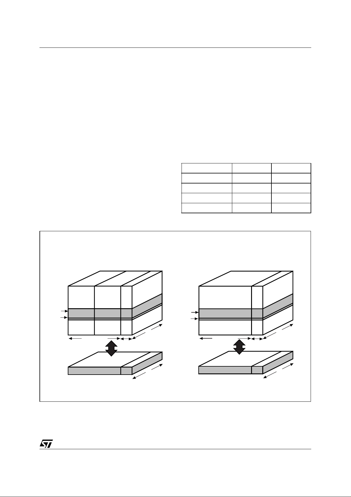
MEMORY ARRAY ORGANIZATION
The memory array is m ade up of N AND struc tures
where 16 cells are connected in series.
The memory array is organized in blocks where
each block contains 32 pages. The array is split
into two areas, the main area and the spare area.
The main area of the array is used to store data
whereas the spare area is typically used to store
Error correction Codes, software flags or Bad
Block identification.
In x8 devices the pages are split into a main area
with two half pages o f 256 Bytes each a nd a spare
area of 16 Bytes. In the x16 dev ices the p ages ar e
split into a 256 Word main area and an 8 Word
spare area. Refer t o Figure 10., Memory Arr ay Or-
ganization.
Bad Blocks
The NAND Flash 528 Byte/ 264 Wor d Page dev ices may contain Bad Blocks, that is blocks that contain one or more invalid bits wh ose reli ability i s not
guaranteed. Additional Bad Blocks may develop
during the lifetime of the device.
Figure 10. Memory Array Organization
The Bad Block Information is written prior to shipping (refer to Bad Block Management section for
more details).
Table 4. shows the minimum number of valid
blocks in each device. The values shown include
both the Bad Blocks that are pre sent when the device is shipped and the Bad Blocks that could develop later on.
These blocks need to be managed using Bad
Blocks Management, Block Replacement or Error
Correction Codes (refer to SOFTWARE ALGO-
RITHMS section).
Table 4. Valid Blocks
Density of Device Min Max
1Gbit 8032 8192
512Mbits 4016 4096
256Mbits 2008 2048
128Mbits 1004 1024
Block
Page
1st half Page
(256 bytes)
512 Bytes
Page Buffer, 512 Bytes
x8 DEVICES x16 DEVICES
Block = 32 Pages
Page = 528 Bytes (512+16)
16
Bytes
16
Bytes
Spare Area
2nd half Page
(256 bytes)
512 Bytes
Block
Page
8 bits
8 bits
Block = 32 Pages
Page = 264 Words (256+8)
Main Area
256 Words
Page Buffer, 264 Words
256 Words
8
Words
8
Words
Spare Area
16 bits
16 bits
AI07587
15/57

NAND128-A, NAND256-A, NAND512-A, NAND01G-A
SIGNAL DESCRIPTIONS
See Figure 2., Logic Diagram, and Table
3., Signal Names, for a brief overview of the sig-
nals connected to this device. Inputs/Outputs (I/O0-I/O7). Input/Outputs 0 to 7
are used to input the selected address, output the
data during a Read operation or input a co mma nd
or data during a Write operation. The inputs are
latched on the rising edge of Write Enable. I/O0-I/
O7 are left floating when the device is deselected
or the outputs are disabled.
Inputs/Outputs (I/O8-I/O15). Input/Outputs 8 to 15 are only available in x16 devices. They are used to output the data duri ng a Read oper ation or input data during a Write operation. Comma nd and Address Inputs only require I/O0 to I/O7.
The inputs are latched on the rising edge of Write
Enable. I/O8-I/O15 are left floating when the device is deselected or the outputs are disabled.
Address Latch Enable (AL). The Address Latch
Enable activates the latching o f the Address inputs
in the Command Interface. When AL is high, the
inputs are latched on the rising edge of Write Enable.
Command Latch Enable (CL). The Command
Latch Enable activates the latching of the Command inputs in the Command Interface. When CL
is high, the inpu ts are l atched on the ri sing e dge of
Write Enable.
Chip Enable (E
). The Chip Enable input acti-
vates the memory control logic, input buffers, decoders and sense ampl ifiers. When Chip Enable is
low, V
, the device is selected.
IL
While the device is busy programming or erasing,
Chip Enable transitions to High, V
, are ignored
IH
and the device does not revert to the Standby
mode.
While the device is busy reading:
■ the Chip Enable input should be held Low
during the whole busy time (t
BLBH1
) for
devices that do not present the Chip Enable
Don’t Care option. Otherwise, the read
operation in progress is interrupted and the
device reverts to the Standby mode.
■ for devices that feature the Chip Enab le Don't
Care option, Chip Enable going High during
the busy time (t
) will not interrupt the
BLBH1
read operation and t he device will not revert to
the Standby mode.
Read Enable (R
). T he Read Enable, R, controls
the sequential data output during Read opera-
tions. Data is valid t
The falling edge of R
after the falling edge of R.
RLQV
also increments the internal
column address counter by one.
Write Enable (W
). The Write Enable input, W,
controls writing to the Command Interface, Input
Address and Data latches. Both addresses and
data are latched on the rising edge of Write Enable.
During power-up and power- down a rec overy time
of 1µs (min) is required before th e Command Interface is ready to accept a command. It is recommended to keep Write Enable high during the
recovery time.
Write Protect (WP
). The Write Protect pin is an
input that gives a hardware protection against unwanted program or erase operations. When Write
Protect is Low, V
, the device does not accept any
IL
program or erase operations.
It is recommended to keep the Write Protect pin
Low, V
Ready/Busy (RB
, during power-up and power-down.
IL
). The Ready/Busy output, RB,
is an open-drain output that can be used to identify
if the P/E/R Controller is currently active.
When Ready/Busy is Lo w, V
, a read, progra m or
OL
erase operation i s in progress . When the oper ation
completes Ready/Busy goes High, V
OH
.
The use of an open- drain output allows the Ready/
Busy pins from several mem ories to be c onnected
to a single pull-up resist or. A Low will then indicate
that one, or more, of the memories is busy.
Refer to the Ready/Busy Signal Electrical Charac-
teristics section for details on how to calculate the
value of the pull-up resistor.
V
Supply Voltage. VDD provides the power
DD
supply to the internal core of the memory device.
It is the main power suppl y for all ope rations (read,
program and erase).
An internal voltage detector disables all functions
whenever V
is below 2.5V (for 3V devices) or
DD
1.5V (for 1.8V devices) to protect the device from
any involuntary program/erase during power-transitions.
Each device in a system sh ould have V
DD
decoupled with a 0.1µF capaci tor . T he PCB tr ac k widths
should be sufficient to carry the required program
and erase currents
V
Ground. Ground, V
SS
is the reference for
SS,
the power supply. It must be connected to the system ground.
16/57

BUS OPERATIONS
NAND128-A, NAND256-A, NAND512-A, NAND01G-A
There are six standard bus oper ati ons that contr ol
the memory. Each of these is described in this
section, see Table 5., Bus Operations, for a sum-
mary.
Command Input
Command Input bus operations are used to give
commands to the memory. Command are accepted when Chip Enable is Low, Command Latch Enable is High, Address Latch Enable is Low and
Read Enable is High. They are latched on the rising edge of the Write Enable signal.
Only I/O0 to I/O7 are used to input commands.
See Fi gure 23. an d Table 20. for d etails of the tim-
ings requirements.
Address Input
Address Input bus operations are used to input the
memory address. T hree bus cycles are r equired to
input the addresses for the 128Mb and 25 6Mb devices and four bus cycles are requi red to input t he
addresses for the 512Mb and 1Gb devices (refer
to Tables 6 and 7, Address Insertion).
The addresses are accepted when Chi p Enab le is
Low, Address Latch Enable is High, Command
Latch Enable is Low and Read Enable is High.
They are latched on the rising edge of the Write
Enable signal. Only I/O0 to I/O7 are used to input
addresses.
See Fi gure 24. an d Table 20. for d etails of the timings requirements.
Data Input
Data Input bus operations are used to input the
data to be programmed.
Data is accepted only when Chip Enable is Low,
Address Latch Enable is Low, Command Latch
Enable is Low and Read Enable is High. The data
is latched on the rising edge of the Write Enable
signal. The data is input sequentially using the
Write Enable signal.
See Fi gure 25. and Table 20. an d Tabl e 21. for details of the timings requirements.
Data Output
Data Output bus operations are used to read: the
data in the memory ar ra y, the Status Register, the
Electronic Signature and the Serial Number.
Data is output when Chip Enabl e is Low, Write Enable is High, Address Latch Enable is Low, and
Command Latch Enable is Low.
The data is output sequentially using the Read Enable signal.
See Fi gure 26. a nd Table 21. for detail s of the tim-
ings requirements.
Write Protect
Write Protect bus operations are used to protect
the memory against program or erase operations.
When the Write Protect signal is Low the device
will not accept program or erase operations and so
the contents of the memory array cannot be altered. The Write Protect signal is not latched by
Write Enable to ensure protection even during
power-up.
Standby
When Chip Enable is High the memory enters
Standby mode, the device is deselected, outputs
are disabled and power consumption is reduced.
Table 5. Bus Operations
Bus Operation E AL CL R W WP I/O0 - I/O7
Command Input
Address Input
Data Input
Data Ou tput
Write Protect X X X X X
Standby
Note: 1. Only for x16 devices.
WP must be VIH when issuing a program or erase command.
2.
V
IL
V
IL
V
IL
V
IL
V
IH
V
V
IH
V
V
XXXXX X X
V
IL
IL
IL
IH
V
IL
V
IL
V
Falling
IL
V
Rising
IH
V
Rising X Address X
IH
V
Rising X Data Input Data Input
IH
V
IH
(2)
X
X Data Output Data Output
V
IL
Command X
I/O8 - I/O15
XX
(1)
17/57

NAND128-A, NAND256-A, NAND512-A, NAND01G-A
Table 6. Address Insertion, x8 Devices
Bus Cycle I/O7 I/O6 I/O5 I/O4 I/O3 I/O2 I/O1 I/O0
st
1
nd
2
rd
3
th(4)
4
Note: 1. A8 is set Low or High by the 00h or 01h Command, see Pointer Operations section.
2. Any additional address input cycles will be ignored.
3. The 4th cycle is only required for 512Mb and 1Gb devices.
Table 7. Address Insertion, x16 Devices
Bus
Cycle
st
1
nd
2
rd
3
th(4)
4
Note: 1. A8 is Don’t Care in x16 devices.
2. Any additional address input cycles will be ignored.
3. The 01h Command is not used in x16 devices.
4. The 4th cycle is only required for 512Mb and 1Gb devices.
A7 A6 A5 A4 A3 A2 A1 A0
A16 A15 A14 A13 A12 A11 A10 A9
A24 A23 A22 A21 A20 A19 A18 A17
V
I/O8-
I/O15
IL
V
IL
V
IL
V
IL
V
IL
V
IL
A26 A25
I/O7 I/O6 I/O5 I/O4 I/O3 I/O2 I/O1 I/O0
X A7 A6 A5 A4 A3 A2 A1 A0
X A16 A15 A14 A13 A12 A11 A10 A9
X A24 A23 A22 A21 A20 A19 A18 A17
X
V
IL
V
IL
V
IL
V
IL
V
IL
V
IL
A26 A25
Table 8. Address Definitions
Address Definition
A0 - A7 Column Address
A9 - A26 Page Address
A9 - A13 Address in Block
A14 - A26 Block Ad dr ess
A8
A8 is set Low or High by the 00h or 01h Command, and is
Don’t Care in x16 devices
18/57

COMMAND SET
NAND128-A, NAND256-A, NAND512-A, NAND01G-A
All bus write operations to the device are int erpreted by the Command Interface. The Commands
are input on I/O0-I/O7 and a re latched on the risi ng
edge of Write Enable when the Command Latch
Enable signal is high. Device operations are selected by writing specific commands to the Com-
mand Register. The two-step command
sequences for program and erase operations are
imposed to maximize data security.
The Commands are summarized in Table
9., Commands.
Table 9. Com m and s
Command
1st CYCLE 2nd CYCLE 3rd CYCLE
Read A 00h - Read B
Read C 50h - -
Read Electronic Si gnature 90h - Read Status Register 70h - - Yes
Page Program 80h 10h Copy Back Program 00h 8Ah 10h
Block Erase 60h D0h Reset FFh - - Yes
Note: 1. The bus cycles are only shown for issuing the codes. The cycles require d to input the addresses or input/out put data are not shown.
2. Any undefined command sequence will be ignored by the devic e.
01h
Bus Write Operations
(2)
- -
(1)
Command accepted
during busy
19/57

NAND128-A, NAND256-A, NAND512-A, NAND01G-A
DEVICE OPERATIONS
Pointer Operations
As the NAND Flash memories contain two different areas for x16 devices and t hree differe nt areas
for x8 devices (see Figur e 11.) the read command
codes (00h, 01h, 50h) are used to act as pointers
to the different area s of the memory arr ay (they select the most significant column address).
The Read A and Read B commands act as pointers to the main memory area. Their use depends
on the bus width of the device.
■ In x16 devices the Read A command (00h)
sets the pointer to Area A (the whole of the
main area) that is Words 0 to 255.
■ In x8 devices the Read A com mand (00h) sets
the pointer to Area A (the first half of the main
area) that is Bytes 0 to 255, and the Read B
command (01h) sets the pointer to Ar ea B (the
Figure 11. Pointer Operations
x8 Devices x16 Devices
Area A
(00h)
Bytes 0- 255 Bytes 256-511
Area B
(01h)
Area C
(50h)
Bytes 512
-527
second half of the main area) th at is Bytes 256
to 511.
In both the x8 and x16 devices the Read C command (50h), acts as a poi nter to Area C (the spar e
memory area) that is Bytes 512 to 527 or Words
256 to 263.
Once the Read A and Read C commands have
been issued the pointer remains in the respective
areas until another pointer c ode is issued. H owever, the Read B command is effective for only one
operation, once an operation has been executed
in Area B the pointer retur ns au tomati cal ly to Ar ea
A.
The pointer operations can also be used before a
program operation, that is the appropriate code
(00h, 01h or 50h) can be issued before the program command 80h is issued (see Figure 12.).
Area A
(00h)
Words 0- 255
Area C
(50h)
Words 256
-263
A
Pointer
(00h,01h,50h)
CB
Page Buffer
A
Pointer
(00h,50h)
C
Page Buffer
AI07592
20/57

NAND128-A, NAND256-A, NAND512-A, NAND01G-A
Figure 12. Pointer Operations for Programming
AREA A
80h
00h
I/O
Areas A, B, C can be programmed depending on how much data is input. Subsequent 00h commands can be omitted.
01h
50h
80h
80h
I/O
Areas B, C can be programmed depending on how much data is input. The 01h command must be re-issued before each program.
I/O
Address
Inputs
Address
Inputs
Address
Inputs
Only Areas C can be programmed. Subsequent 50h commands can be omitted.
Data Input
Data Input
Data Input
10h
AREA B
10h
AREA C
10h
00h
01h
50h
80h
80h
80h
Address
Inputs
Address
Inputs
Address
Inputs
Data Input
Data Input
Data Input
10h
10h
10h
ai07591
21/57

NAND128-A, NAND256-A, NAND512-A, NAND01G-A
Read Memory Array
Each operation to read the memory area starts
with a pointer operation as shown in the Pointer
Operations section. Once the area (main or spare)
has been selected using the Read A, Read B or
Read C commands four bus cycles (for 512Mb
and 1Gb devices) or three bus cycles (for 128Mb
and 256Mb devices) are required to input the address (refer to Table 6.) of the data to be read.
The device defaults to Read A mode after powerup or a Reset operation.
When reading the spare area addresses:
■ A0 to A3 (x8 devices)
■ A0 to A2 (x16 devices)
are used to set the start address of the spare area
while addresses:
■ A4 to A7 (x8 devices)
■ A3 to A7 (x16 devices)
are ignored.
Once the Read A or Read C commands have
been issued they do not need to be reissued for
subsequent read operations as the pointer remains in the respective area. However, the Read
B command is effective for only one operation,
once an operation has been executed in Area B
the pointer returns automatically to Area A and so
another Read B command is required to start another read operation in Area B.
Once a read command is issued th ree types of operations are available : Ran dom R ead, Pa ge Re ad
and Sequential Row Read.
Random Read. Each time the command is issued the first read is Random Read.
Page Read. After the Random Read access the
page data is transferred to the Page Buffer in a
time of
t
(refer to Table 21. for value). Once
WHBH
the transfer is complete the Ready/Busy signal
goes High. The data can then be read out sequentially ( from se lected column a ddress to last column
address) by pulsing the Read Enable signal.
Sequential Row Read. After the data in last column of the page is output, if the Read Enable signal is pulsed and Chip Enable remains Low then
the next page is automatically loaded into the
Page Buffer and the read operation continues. A
Sequential Row Read operation can only be used
to read within a block. If the block changes a new
read command must be issued.
Refer to Figure 15. and F igure 16. for details of Sequential Row Read operations.
To terminate a Seque ntial Row Read ope ration set
the Chip Enable sig nal to High for m ore than t
EHEL
Sequential Row Read is not available when the
Chip Enable Don't Care option is enabled.
.
22/57

Figure 13. Read (A,B,C) Operations
CL
E
W
AL
R
RB
NAND128-A, NAND256-A, NAND512-A, NAND01G-A
tBLBH1
(read)
I/O
00h/
01h/ 50h
Command
Code
Address Input
Figure 14. Read Block Diagrams
Read A Command, X8 Devices
Area A
(1st half Page)
(1)
A9-A26
A0-A7
Read B Command, X8 Devices
Area A
(1st half Page)
(1)
A9-A26
A0-A7
Note: 1. Highest address depends on device density.
Area B
(2nd half Page)
Area B
(2nd half Page)
Area C
(Spare)
Area C
(Spare)
Busy
A9-A26
A0-A7
(1)
A9-A26
A0-A3 (x8)
A0-A2 (x16)
Data Output (sequentially)
Read A Command, X16 Devices
Area A
(main area)
(1)
Read C Command, X8/x16 Devices
Area A
A4-A7 (x8), A3-A7 (x16) are don't care
Area A/ B
ai07595
Area C
(Spare)
Area C
(Spare)
AI07596
23/57

NAND128-A, NAND256-A, NAND512-A, NAND01G-A
Figure 15. Sequential Row Read Operations
RB
I/O
00h/
01h/ 50h
Command
Code
tBLBH1
(Read Busy time)
Address Inputs
Busy
tBLBH1 tBLBH1
1st
Page Output
Figure 16. Sequential Row Read Block Diagrams
Read A Command, x8 Devices
Area A
(1st half Page)
Block
Read B Command, x8 Devices Read C Command, x8/x16 Devices
Area A
(1st half Page)
Block
Area B
(2nd half Page)
Area B
(2nd half Page)
Area C
(Spare)
Area C
(Spare)
1st page
2nd page
Nth page
1st page
2nd page
Nth page
2nd
Page Output
Read A Command, x16 Devices
Area A
(main area)
Block
Area A Area A/ B Area C
Block
BusyBusy
Nth
Page Output
Area C
(Spare)
1st page
2nd page
Nth page
(Spare)
1st page
2nd page
Nth page
ai07597
AI07598
24/57

NAND128-A, NAND256-A, NAND512-A, NAND01G-A
Page Program
The Page Program oper ation is the standard op eration to program data to the memory array.
The main area of the memory array is programmed by page, however pa rtial page progr amming is allowed where any number of bytes (1 to
528) or words (1 to 264) can be programmed.
The maximum number of cons ecut ive parti al pa ge
program operations allowed in the same page is
three. After exceeding this a Block Erase command must be issued before any further program
operations can take place in that page.
Before starting a Pag e Program operati on a Pointer operation can be perfo rme d to poi nt to the ar ea
to be programmed. Refer to the Pointer Opera-
tions section and Figure 12. for details.
Each Page Program operation consists of five
steps (see Figure 17.):
1. one bus cycle is required to setup the Page
Program command
2. four bus cycles are then required to input the
program address (refer to Table 6.)
Figure 17. Page Program Operation
3. the data is then input (up to 528 Bytes/ 264
Words) and loaded into the Page Buffer
4. one bus cycle is required to issue the confirm
command to start the P/E/R Controller.
5. T he P/E/R Controller then programs the data
into the array.
Once the program operation has started the Status Register can be read using the Read Status
Register command. During program operations
the Status Register will only flag errors for bits set
to '1' that have not been s uccessfull y progr ammed
to '0'.
During the program operation, only the Read Status Register and Reset commands will be accepted, all other commands will be ignored.
Once the program operatio n has completed the P/
E/R Controller bit SR6 is set to ‘1’ and the Ready/
Busy signal goes High.
The device remai ns in Read Status Register mode
until another valid com mand is w ritten to the C ommand Interface.
tBLBH2
RB
I/O
Note: Before starting a Page Program operation a Pointer operation can be performed. Refer to Pointer Operations section for details.
80h
Page Program
Setup Code
Address Inputs
Data Input
(Program Busy time)
10h
Confirm
Code
Busy
70h
Read Status Register
SR0
ai07566
25/57

NAND128-A, NAND256-A, NAND512-A, NAND01G-A
Copy Back Program
The Copy Back Program opera tion is used to copy
the data stored in one page an d reprogram it in another page.
The Copy Back Program operation does not require external memory and so the operation is
faster and more efficient because the reading and
loading cycles are not required. The operation is
particularly useful when a portion of a block is updated and the rest of t he bl oc k ne eds to be co pi ed
to the newly assigned block.
If the Copy Back Program operation fails an error
is signalled in the Status Register. However as the
standard external ECC cannot be used with the
Copy Back operation bit error due to charge loss
cannot be detected. For this reason it is recommended to limit the number of Copy Back operations on the same data and or to improve the
performance of the ECC.
The Copy Back Program operation requires three
steps:
1. The source page mu st be read using the Read
A command (one bus write cycle to setup the
command and then 4 bus write cycles to input
the source page address). This operation
copies all 264 Words/ 528 Bytes fr om the page
into the Page Buffer.
2. When the device returns to the ready state
(Ready/Busy High), the second bus write
cycle of the command is given with the 4 bus
cycles to input the target page addr ess. Refer
to Table 10. for th e addresses that mu st be the
same for the Source and Target pages.
3. T hen the confirm command is issued to start
the P/E/R Controller.
After a Copy Back Program operation, a partialpage program is not allowed in the target page until the block has been erased.
See Figure 18. for an example of the Copy Back
operation.
Table 10. Copy Back Program Addresses
Density
128 Mbit A23
256 Mbit A24
512 Mbit A25
512 Mbit DD
1 Gbit DD
Note: 1. DD = Dual Die.
(1)
Same Address for Source and
(1)
Target Pages
A24, A25
A25, A26
Figure 18. Copy Back Operation
tBLBH1
RB
I/O
Read
Code
(Read Busy time)
Source
Address Inputs
8Ah 70h00h
Copy Back
Code
(Program Busy time)
Target
Address Inputs
tBLBH2
10h
Busy
SR0
Read Status Register
ai07590b
26/57

NAND128-A, NAND256-A, NAND512-A, NAND01G-A
Block Erase
Erase operations are d one one blo ck at a time. An
erase operation sets all of the bits in the addressed block to ‘1’. All previous data in the block
is lost.
An erase operation consists of three steps (refer to
Figure 19.):
1. One bus cycle is required to setup the Block
Erase command.
2. Only three bus cycles for 512Mb and 1Gb
devices, or two for 128Mb and 256Mb devices
Figure 19. Block Erase Operation
RB
I/O
60h
Block Erase
Setup Code
Block Address
Inputs
are required to input the block address. The
first cycle (A0 to A7) is not required as only
addresses A14 to A26 (highest address
depends on device density) are valid, A9 to
A13 are ignored. In the last address cycle I/O2
to I/O7 must be set to V
.
IL
3. One bus cycle is required to issue th e confirm
command to start the P/E/R Controller.
Once the erase operation has completed the Status Register can be checked for errors.
tBLBH3
(Erase Busy time)
Busy
D0h
Confirm
Code
70h
Read Status Register
SR0
ai07593
Reset
The Reset command is used to reset the Command Interface and Status Register. If the Reset
command is issued during any operation, the operation will b e aborted. I f it was a program or eras e
operation that was aborted, the contents of the
memory locations bei ng modi fied w i ll no longer be
valid as the data will be partially programmed or
erased.
If the device has already been reset then the new
Reset command will not be accepted.
The Ready/Busy signal goes Low for t
the Reset command is i ssued. The val ue of t
BLBH4
after
BLBH4
depends on the operation that th e device wa s performing when the command was issued, refer to
Table 21. for the values.
27/57

NAND128-A, NAND256-A, NAND512-A, NAND01G-A
Read Status Register
The device contains a Status Register which provides information on the current or previous Program or Erase operation. The various bits in the
Status Register convey information and errors on
the operation.
The Status Register is read by issuing the Read
Status Register command. The Status Re gister information is present on the output data bus (I/O0I/O7) on the falling edge of Chip Enable or Read
Enable, whichever occurs last. When several
memories are connected in a system, the use of
Chip Enable and Read Enable signals allows the
system to poll each device separately, even when
the Ready/Busy pins are common-wired. It is not
necessary to toggle the Chip Enable or Read Enable signals to update the contents of the Status
Register.
After the Read Status Register command has
been issued, the device remains in Read Status
Register mode until another command is issued.
Therefore if a Read Status Register command is
issued during a Random Read cycle a new read
command must be issued to conti nue with a Page
Read or Sequential Row Read operation.
The Status Register bits are summarized in Table
11., Status Register Bits. Refer to Table 11. in
conjunction with the following text descriptions.
Write Protection Bit (SR7). The Write Protection
bit can be used to identify if the devi ce is protected
or not. If the W rite Pro tection b it is set to ‘1’ the device is not protected and program or erase operations are allowed. If the Write Protection bit is set
to ‘0’ the device is protected and pro gram or erase
operations are not allowed.
P/E/R Controller Bit (SR6). The Program/Erase/
Read Controller bit indicates whether the P/E/R
Controller is active or inactive. When the P/E/R
Controller bit is set to ‘0’, the P/E/R Controller is
active (device is busy ); when the bit is set to ‘1’, the
P/E/R Controller is inactive (device is ready).
Error Bit (SR0). The Error bit is used to identify if
any errors have been detected by the P/E/R Controller. The Error Bit is set to ’1’ w hen a program or
erase operation has faile d to write the correct d ata
to the memory. If the Error Bit is set to ‘0’ the operation has completed successfully.
SR5, SR4, SR3, SR2 and SR1 are Reserved.
28/57

NAND128-A, NAND256-A, NAND512-A, NAND01G-A
Table 11. Status Register Bits
Bit Name Logic Level Definition
SR7 Write Protection
SR6
SR5, SR4,
SR3, SR2, SR1
SR0 Generic Error
Program/ Erase/ Read
Controller
Reserved
'1' Not Protected
'0' Protected
'1' P/E/R C inactive, device ready
'0' P/E/R C active, device busy
Don’t Care
‘1’ Error – operation failed
‘0’ No Error – operation successful
Read Electronic Signature
The d ev i c e co n t ai n s a Manuf acture r Code and Device Code. To read these codes two steps are required:
1. first use one Bus Write cycle to issue the Read
Electronic Signature command (90h)
2. then perform two Bus Read operations – the
first will read the Manufacturer Code and the
second, the Device Code. Further Bus Read
operations will be ignored.
Refer to Table 12., Electronic Signature, for infor-
mation on the addresses.
Table 12. Electronic Si gnature
Part Number
NAND128R3A
NAND128W3A 73h
NAND128R4A
NAND128W4A 0053h
NAND256R3A
NAND256W3A 75h
NAND256R4A
NAND256W4A 0055h
NAND512R3A
NAND512W3A 76h
NAND512R4A
NAND512W4A 0056h
NAND01GR3A
NAND01GW3A 79h
NAND01GR4A
NAND01GW4A 0059h
Manufacturer
Code
20h
0020h
20h
0020h
20h
0020h
20h
0020h
Device code
33h
0043h
35h
0045h
36h
0046h
39h
0049h
29/57

NAND128-A, NAND256-A, NAND512-A, NAND01G-A
SOFTWARE ALGORITHMS
This section gives information on the software algorithms that ST recommends to implement to
manage the Bad Blocks and extend the lifetime of
the NAND device.
NAND Flash memories are programmed and
erased by Fowler-N ordheim tunneling u sing a high
voltage. Exposing the device to a high voltage for
extended periods can cause the oxide layer to be
damaged. For this rea son , the num ber of pro gram
and erase cycles is limited (see Table 14. for value) and it is recommended to implement Garbage
Collection, a Wear-Leveling Algorithm and an Error Correction Code, to extend the number of program and erase cycles and increase the data
retention.
To help integrate a NAND memor y into an a pplication ST Microelectronics can provide:
■ File System OS Native reference software,
which supports the basic commands of file
management.
Contact the nearest ST Microelectronics sales office for more details.
Bad Block Manage ment
Devices with Bad Blocks have the same quality
level and the same AC and DC characteristics as
devices where all the blocks ar e valid. A Bad Block
does not affect the p erformanc e of valid blocks because it is isolated from the bit line and common
source line by a select transistor.
The devices are supplied with all the locations inside valid blocks erased (FFh). The Ba d Block Information is written prior to shipping. Any block
where the 6th Byte/ 1st Word in the spare area of
the 1st page does not contain FFh is a Bad Block.
The Bad Block Information must be read before
any erase is attempted as the Bad Block Information may be erased. For the system to be able to
recognize the Bad Blocks ba sed on th e origina l information it is recommended to create a Bad Block
table following the flowchart shown in Figure 20.
Block Replacement
Over the lifetime of the device additional Bad
Blocks may develop. In this case the block has to
be replaced by copying the data to a valid block.
These additional Bad Blocks can be identified as
attempts to program or erase them will give er r ors
in the Status Register.
As the failure of a page program operation does
not affect the data in other pages in the same
block, the block can be replaced by re-programming the current data and copying the rest of the
replaced block to an available valid block. The
Copy Back Program command can be used to
copy the data to a valid block.
See the “Copy Back Program” section for more details.
Refer to Table 13. for the recommended procedure to follow if an error occurs during an operation.
Table 13. Block Failure
Operation Recommended Procedure
Erase Block Replacement
Program Block Replacement or ECC
Read ECC
Figure 20. Bad Block Management Flowchart
START
Block Address =
Block 0
Data
= FFh?
YES
Last
block?
YES
END
NO
NO
Increment
Block Address
Update
Bad Block table
AI07588C
30/57

Figure 21. Garbage Collection
2
NAND128-A, NAND256-A, NAND512-A, NAND01G-A
Old Area
Valid
Page
Invalid
Page
Garbage Collection
When a data page needs to be modified, i t is faster
to write to the first available page, and the previous
page is marked as invalid. After sever al updates it
is necessary to remove invalid pa ges to free s ome
memory space.
To free this memory space and allow further program operations it is recommended to implement
a Garbage Collection algo rithm. In a Garba ge Collection software the valid pages are copied into a
free area and the bloc k c ontai ning the invalid pages is erased (see Figure 21.).
Wear-leveling Algorithm
For write-intensive applications, it is recommended to implement a Wear-leveling Algorithm to
monitor and spread the number of writ e cycles per
block.
In memories that do not use a Wear-L ev eling Algorithm not all blocks get used at the same rate.
Blocks with long- liv ed dat a do not endu re as man y
write cycles as the bloc ks with freque ntly-c hanged
data.
The Wear-leveling Algorithm ensures that equal
use is made of all the available write cycles for
each block. There are two wear-leveling levels:
■ First Level Wear-leveling, new data is
programmed to the free blocks that have had
the fewest write cycles
■ Second Level Wear-lev eling, long-lived da ta is
copied to another block so that the original
block can be used for more frequentlychanged data.
The Second Level Wear-l eveling is triggere d when
the difference be tween the maximu m and th e minimum number of write cycles per block reaches a
specific threshold.
New Area (After GC)
Free
Page
(Erased)
AI07599B
Error Correction Code
An Error Correction Code (ECC) can be implemented in the Nand Flash memories to identify
and correct errors in the data.
For every 2048 bits in the de vic e i t i s rec om mended to implement 22 bits of ECC (16 bits for line parity plus 6 bits for column parity).
An ECC model is available in VHDL or Verilog.
Contact the nearest ST Microelectronics sales office for more details.
Figure 22. Error Detection
New ECC generated
during read
XOR previous ECC
with new ECC
All results
= zero?
YES
22 bit data = 0
No Error
NO
YES
11 bit data = 1
Correctable
>1 bit
= zero?
Error
NO
1 bit data = 1
ECC Error
ai0833
31/57

NAND128-A, NAND256-A, NAND512-A, NAND01G-A
Hardware Simulation Models
Behavioral simulation models. Denali Software
Corporation models are platform independent
functional models designed to assist customers in
performing entire system simulations (typical
VHDL/Verilog). These models describe the logic
behavior and timings of NAND Flas h devi ce s, and
so allow software to be developed before hardware.
IBIS simulations models. IBIS (I/O Buffer Information Specification) models describe the behav-
ior of the I/O buffers and electrical characteristics
of Flash devices.
These models provide information such as AC
characteristics, rise/fall times and package mechanical data, all of which are measured or simulated at voltage and temperature ranges wider
than those allowed by target specifications.
IBIS models are used to simulate PCB connections and can be used to resolve compatibility issues when upgrading devices. They can be
imported into SPICETOOLS.
32/57

NAND128-A, NAND256-A, NAND512-A, NAND01G-A
PROGRAM AND ERASE TIMES AND ENDURANCE CYCLES
The Program and Erase times and the number of
Program/ Erase cycles pe r block are shown in Ta-
ble 14.
Table 14. Program, Erase Times and Program Erase Endurance Cycles
Parameters
Min Typ Max
Page Program Time 200 500 µs
Block Erase Time
Program/Erase Cycles (per block) 100,000 cycles
Data Retention 10 years
NAND Flash
Unit
2 3ms
MAXIMUM RATING
Stressing the device above the ratings listed in Ta-
ble 15., Absolute Maximum Ratings, may cause
permanent damage to the device. These are
stress ratings only and operation of the device at
these or any other conditions abov e tho se ind icat-
not implied. Exposure to Absolute Maximum Rating conditions for ex tend ed p eri ods may affect device reliability. Refer also to the
STMicroelectronics SURE Program and other relevant quality documents.
ed in the Operating sections of this specif icatio n is
Table 15. Absolute Maximum Ratings
Symbol Parameter
T
BIAS
T
STG
(1)
VIO
V
DD
Note: 1. Minimum Voltage may undershoot to –2V for less than 20ns during transitions on input and I/O pins. Maximum voltage may over-
shoot to V
Temperature Under Bias – 50 125 °C
Storage Temperature – 65 150 °C
Input or Output Voltage
Supply Voltage
+ 2V for less than 20ns during transitions on I/O pins.
DD
1.8V devices – 0.6 2.7 V
3 V devices – 0.6 4.6 V
1.8V devices – 0.6 2.7 V
3 V devices – 0.6 4.6 V
Value
Unit
Min Max
33/57

NAND128-A, NAND256-A, NAND512-A, NAND01G-A
DC AND AC PARAMETERS
This section summarizes the operating and measurement conditions, and the DC and AC characteristics of the device. The parameters in the DC
and AC characteristics Tables that follow, are derived from tests performed under the Measure-
ment Conditions summarized in Table
16., Operating and AC Measurement Conditions.
Designers should check that the operating conditions in their circuit match the measurem ent conditions when relying on the quoted parameters.
Table 16. Operating and AC Measurement Conditions
Parameter
Supply Voltage (V
Ambient Temperature (T
Load Capacitance (C
Input Pulses Voltage s
Input and Output Timing Ref. Voltages
Input Rise and Fall Times 5 ns
Output Circuit Resistors, R
)
DD
)
A
) (1 TTL GATE and CL)
L
ref
1.8V devices 1.7 1.95 V
3V devices 2.7 3.6 V
Grade 1 0 70 °C
Grade 6 –40 85 °C
1.8V devices 30 pF
3V devices (2.7 - 3.6V) 50 pF
3V devices (3.0 - 3.6V) 100 pF
1.8V devices 0
3V devices 0.4 2.4 V
1.8V devices 0.9 V
3V devices 1.5 V
NAND Flash
Min Max
V
DD
8.35 kΩ
Units
V
Table 17. Ca pacitance
Symbol Parameter Test Condition Typ Max Unit
C
IN
C
I/O
Note: TA = 25°C, f = 1 MHz. CIN and C
34/57
Input Capacitance
Input/Output Capacitance
are not 100% tested.
I/O
V
V
IN
IL
= 0V
= 0V
10 pF
10 pF

NAND128-A, NAND256-A, NAND512-A, NAND01G-A
Table 18. DC Characteristics, 1.8V Devices
Symbol Parameter Te st Cond itions Min Typ Max Unit
t
I
DD1
I
DD2
I
DD3
I
DD5
I
LI
I
LO
V
IH
V
IL
V
OH
V
OL
IOL (RB)
V
LKO
Sequential
Operating
Current
Read
Program - - 8 15 mA
E
Erase - - 8 15 mA
Stand-By Curre n t (CMOS)
128Mb, 256Mb, 512Mb devices
Stand-By Curre n t (CMOS)
512Mb and 1Gb Dua l Die devices
Input Leakage Current
Output Leakage Current
V
Input High Voltage Input Low Voltage - -0.3 - 0.4 V
Output High Voltage Level
Output Low Voltage Level
Output Low Current (RB)
VDD Supply Voltage (Erase and
Program lockout)
minimum
RLRL
=V
IL, IOUT
= 0 mA
E=VDD-0.2,
=0/V
WP
DD
VIN= 0 to VDDmax
= 0 to VDDmax
OUT
VDD-0.4
IOH = -100µA VDD-0.1
IOL = 100µA
V
= 0.2V
OL
- - - 1.5 V
- 8 15 mA
- 10 50 µA
- 20 100 µA
- - ±10 µA
- - ±10 µA
-
VDD+0.3
- - V
- - 0.1 V
3 4 mA
V
35/57

NAND128-A, NAND256-A, NAND512-A, NAND01G-A
Table 19. DC Characteristics, 3V Devices
Symbol Parameter Te st Cond itions Min Typ Max Unit
t
I
DD1
I
DD2
I
DD3
I
DD4
I
DD5
I
LI
I
LO
V
IH
V
IL
V
OH
V
OL
IOL (RB)
V
LKO
Sequential
Operating
Current
Read
Program - - 10 20 mA
E
Erase - - 10 20 mA
Stand-by Current (TT L) ,
128Mb, 256Mb, 512Mb devices
E=VIH, WP=0V/V
Stand-by Curre nt (TTL)
512Mb and 1Gb Dua l Die devices
Stand-By Curre n t (CMOS)
128Mb, 256Mb, 512Mb devices
Stand-By Curre n t (CMOS)
512Mb and 1Gb Dua l Die devices
Input Leakage Current
Output Leakage Current
V
Input High Voltage - 2.0 Input Low Voltage - −0.3 - 0.8 V
Output High Voltage Level
Output Low Voltage Level
Output Low Current (RB)
VDD Supply Voltage (Erase and
Program lockout)
minimum
RLRL
=V
IL, IOUT
= 0 mA
E=VDD-0.2,
WP
=0/V
DD
VIN= 0 to VDDmax
= 0 to VDDmax
OUT
IOH = −400µA
IOL = 2.1mA
V
= 0.4V
OL
- - - 2.5 V
- 10 20 mA
- - 1 mA
DD
- - 2 mA
- 10 50 µA
- 20 100 µA
- - ±10 µA
- - ±10 µA
VDD+0.3
2.4 - - V
- - 0.4 V
8 10 mA
V
36/57

NAND128-A, NAND256-A, NAND512-A, NAND01G-A
Table 20. AC Characteristics for Command, Address, Data Input
Symbol
t
ALLWL
t
ALHWL
t
CLHWL
t
CLLWL
t
DVWH
t
ELWL
t
WHALH
t
WHALL
t
WHCLH
t
WHCLL
t
WHDX
t
WHEH
t
WHWL
t
WLWH
t
WLWL
Note: 1. If t
Alt.
Symbol
t
ALS
t
CLS
t
DS
t
CS
t
ALH
t
CLH
t
DH
t
CH
t
WH
t
WP
t
WC
is less than 10ns, t
ELWL
Parameter
Address Latch Low to Write Enable Low
AL Setup time Min 0 0 ns
Address Latch High to Writ e E nable Low
Command Latch High to Write Enable Low
CL Setup time Min 0 0 ns
Command Latch Low to Write Enable Low
Data Valid to Write Enable High Data Setup time Min 20 20 ns
Chip Enable Low to Write Enable Low E Setup time Min 0 0 ns
Write Enable High to Address Lat ch H igh
AL Hold time Min 10 10 ns
Write Enable High to Address Lat ch Low
Write Enable High to Command Latch High
CL hold time Min 10 10 ns
Write Enable High to Command Latch Low
Write Enable High to Data Transition Data Hold time Min 10 10 ns
Write Enable High to Chip Enable High E Hold time Min 10 10 ns
Write Enable High to Write Enable Low
W High Hold
time
Write Enable Low to Write Enable High W Pulse Width Min 40
Write Enable Low to Write Enable Low Write Cycle time Min 60 50 ns
must be minimum 35ns, otherwise, t
WLWH
may be minimum 25ns.
WLWH
1.8V
Devices
3V
Devices
Unit
Min 20 15 ns
(1)
25
ns
37/57

NAND128-A, NAND256-A, NAND512-A, NAND01G-A
Table 21. AC Characteristics for Operations
Symbol
t
ALLRL1
t
ALLRL2
t
BHRL
t
BLBH1
t
BLBH2
t
BLBH3
t
BLBH4
Alt.
Symbol
t
AR
t
RR
t
PROG
t
BERS
Parameter
Address Latch Low to
Read Enable Low
Read Electronic Si gnature Min 10 10 ns
Read cycle Min 10 10 ns
Ready/Busy High to Read Enable Low Min 20 20 ns
Ready/Busy Low to
Ready/Busy High
Read Busy time, 128Mb, 256Mb,
512Mb Dual Die
Read Busy time, 512Mb, 1Gb Max 15 12 µs
Program Busy time Max 500 500 µs
Max 12 12 µs
Erase Busy time Max 3 3 ms
Reset Busy time, during re ady Max 5 5 µs
Reset Busy time, during re ad Max 5 5 µs
t
WHBH1
t
Write Enable High t o
RST
Ready/Busy High
Reset Busy time, during program Max 10 10 µs
Reset Busy time, during era se Max 500 500 µs
t
CLLRL
t
DZRL
t
EHBH
t
EHEL
t
EHQZ
t
ELQV
t
RHBL
t
RHRL
t
RHQZ
t
RLRH
t
RLRL
t
RLQV
t
WHBH
t
WHBL
t
WHRL
t
WLWL
Note: 1. The time to Ready depends on the value of the pull-up resistor tied to the Ready/Busy pin. See Figures 34, 35 and 36.
2. To break the sequential read cycle, E
3. ES = Electronic Signature.
t
CLR
t
t
CRY
t
CEH
t
CHZ
t
CEA
t
t
REH
t
RHZ
t
t
RC
t
REA
t
WB
t
WHR
t
WC
Command Latch Low to Read Enable Low Min 10 10 ns
Data Hi-Z to Read Enable Low Min 0 0 ns
IR
Chip Enable High to Ready/Busy High (E intercepted read) Max
Chip Enable High to Chip Enable Low
(2)
Min 100 100 ns
Chip Enable High to Output Hi-Z Max 20 20 ns
Chip Enable Low to Output Valid Max 45 45 ns
Read Enable High to Ready/Bu sy Low Max 100 100 ns
RB
Read Enable High to
Read Enable Low
Read Enable High to Output Hi-Z
Read Enable Low to
RP
Read Enable High
Read Enable Low to
Read Enable Low
Read Enable Low to
Output Valid
Write Enable High t o
t
R
Ready/Busy High
Read Enable High Hold time Min 15 15 ns
Min 15 15
Max 30 30
Read Enable Pulse Width Min 30 30 ns
Read Cycle time Min 60 50 ns
Read Enable Access time
Read ES Access time
(3)
Read Busy time, 128Mb, 256Mb,
512Mb Dual Die
Max 35 35 ns
Max 12 12 µs
Read Busy time, 512Mb, 1Gb Max 15 12 µs
Write Enable High t o Ready/Bu sy Low Max 100 100 ns
Write Enable High t o Read Enable Low Min 80 60 ns
Write Enable Low t o
Write Enable Low
Write Cycle time Min 60 50 ns
must be held High for longer than t
EHEL
.
1.8V
Devices
(1)
60 + t
r
3V
Devices
60 + t
Unit
(1)
ns
r
ns
38/57

NAND128-A, NAND256-A, NAND512-A, NAND01G-A
Figure 23. Comma nd Latch AC Waveforms
CL
tCLHWL
(CL Setup time) (CL Hold time)
tELWL
(E Setup time)
E
W
tALLWL tWHALH
(ALSetup time) (AL Hold time)
AL
tDVWH tWHDX
(Data Setup time) (Data Hold time)
I/O
Figure 24. Address Latch AC Waveforms
tCLLWL
CL
(CL Setup time)
Command
tWLWH
tWHCLL
tWHEH
(E Hold time)
ai08028
tELWL tWLWL
(E Setup time)
E
tWLWH
W
tALHWL
(AL Setup time)
tWHWL
tWHALL
(AL Hold time)
tWHWL
tWHALL
AL
tDVWH
tWHDX
(Data Hold time)
I/O
tDVWH
(Data Setup time)
Adrress
cycle 1
Note: Address cycle 4 is only required for 512Mb and 1Gb devices.
tWLWL tWLWL
tWHWL
tWHALL
tDVWH
tWHDX
Adrress
cycle 2
Adrress
cycle 3
tWLWHtWLWH tWLWH
tDVWH
tWHDX
Adrress
cycle 4
tWHDX
ai08029
39/57

NAND128-A, NAND256-A, NAND512-A, NAND01G-A
Figure 25. Data Input Latch AC Waveforms
CL
E
tALLWL tWLWL
(ALSetup time)
AL
tWHCLH
(CL Hold time)
tWHEH
(E Hold time)
tWLWH
tWLWH
W
I/O
tDVWH
(Data Setup time)
Data In 0 Data In 1
tDVWH
tWHDX
(Data Hold time)
tDVWH
tWHDX
Figure 26. Sequential Data Output after Read AC Waveforms
tRLRL
(Read Cycle time)
E
tRHRL
(R High Holdtime)
R
tRHQZ
tRLQV
(R Accesstime)
tRLQV
Data In
Last
tEHQZ
tRLQV
tWLWH
tWHDX
ai08030
tRHQZ
I/O
tBHRL
RB
Note: 1. CL = Low, AL = Low, W = High.
40/57
Data Out Data Out Data Out
ai08031

NAND128-A, NAND256-A, NAND512-A, NAND01G-A
Figure 27. Read Status Register AC Waveform
CL
tCLHWL
E
tCLLRL
tWHCLL
tWHEH
W
R
I/O
tELWL
tDVWH
(Data Setup time)
70h
tWLWH
tWHDX
(Data Hold time)
Figure 28. Read Electronic Signature AC Waveform
CL
E
W
tWHRL
tDZRL
tELQV
tRLQV
tEHQZ
tRHQZ
Status Register
Output
ai08032
AL
tALLRL1
R
tRLQV
(Read ES Access time)
I/O
Note: Refer to Table 12. for the values of the Manufacturer and Device Codes.
90h 00h
Read Electronic
Signature
Command
1st Cycle
Address
Man.
code
Manufacturer and
Device Codes
Device
code
ai08039b
41/57

NAND128-A, NAND256-A, NAND512-A, NAND01G-A
Figure 29. Page Read A/ Read B Operation AC Waveform
CL
E
tWLWL
W
tEHEL
tEHQZ
tWHBL
AL
tWHBH tRLRL
R
tBLBH1
RB
I/O
Note: Address cycle 4 is only required for 512Mb and 1Gb devices.
00h or
Command
Code
01h
Add.N
cycle 1
Add.N
cycle 2
Address N Input
cycle 3
Add.N
Add.N
cycle 4
tALLRL2
(Read Cycle time)
tRLRH
DataNData
Busy
from Address N to Last Byte or Word in Page
N+1
Data
N+2
Data Output
tEHBH
tRHQZ
tRHBL
Data
Last
ai08033b
42/57

NAND128-A, NAND256-A, NAND512-A, NAND01G-A
Figure 30. Read C Operation, One Page AC Waveform
CL
E
W
tWHALL
AL
R
tWHBH
tALLRL2
tBHRL
Add. M
I/O
RB
Note: 1. A0-A7 is the address in the Spare Memory area, where A0-A3 are valid and A4-A7 are ‘don’t care’.
50h
Command
Code
cycle 1
Add. M
Address M Input
cycle 2
Add. M
cycle 3
Add. M
cycle 4
Busy
Data M
Data Output from M to
Last Byte or Word in Area C
Data
Last
ai08035
43/57

NAND128-A, NAND256-A, NAND512-A, NAND01G-A
Figure 31. Page Program AC Waveform
CL
E
tWLWL tWLWL tWLWL
(Write Cycle time)
W
AL
R
tWHBL
tBLBH2
(Program Busy time)
Add.N
I/O
RB
Note: Address cycle 4 is only required for 512Mb and 1Gb devices.
80h
Page Program
Setup Code
cycle 1
Add.N
cycle 2
Address Input Data Input
Add.N
cycle 3
Add.N
cycle 4
N
Last
10h
Confirm
Code
Page
Program
SR0
70h
Read Status Register
ai08037
44/57

Figure 32. Block Erase AC Waveform
CL
E
tWLWL
(Write Cycle time)
W
NAND128-A, NAND256-A, NAND512-A, NAND01G-A
tWHBL
AL
R
I/O
RB
Block Erase
Setup Command
Note: Address cycle 3 is required for 512Mb and 1Gb devices only.
Add.
cycle 1
Add.
cycle 2
Block Address Input
Add.
cycle 3
Confirm
Figure 33. Reset AC Waveform
W
AL
D0h60h
Code
tBLBH3
(Erase Busy time)
Block Erase
70h
Read Status Register
SR0
ai08038b
I/O
RB
CL
R
FFh
tBLBH4
(Reset Busy time)
ai08043
45/57

NAND128-A, NAND256-A, NAND512-A, NAND01G-A
Ready/Busy Signal Electrical Characteristics
Figures 35, 34 and 36 show the electrical characteristics for the Ready/Busy signal. The value required for the resistor R
can be calculated using
P
the following equation:
Figure 35. Ready/Busy Load Circuit
–()
I
+
I
OL
L
RPmin
V
DDmaxVOLmax
------------------------------------------------------------=
So,
1.85V
---------------------------=
+
3mA I
3.2V
---------------------------=
+
8mA I
L
L
where I
R
min 1.8 V()
P
R
min 3V()
P
is the sum of the input currents of all the
L
devices tied to the Ready/Busy signal. R
determined by the maximum value of t
.
r
Figure 34. Ready/Busy AC Waveform
ready V
DD
V
OL
busy
t
f
V
t
r
max is
P
OH
AI07564B
V
DD
DEVICE
V
SS
R
P
RB
Open Drain Output
ibusy
AI07563B
Figure 36. Resistor Value Versus Waveform Timings For Ready/Busy Signal
VDD = 1.8V, CL = 30pF VDD = 3.3V, CL = 100pF
400
300
(ns)
f
200
, t
r
t
100
0
1234
Note: T = 25°C.
46/57
30
1.7
1.7
0.85
60
1.7
RP (KΩ)
90
0.57
1.7
4
3
(mA)
2
ibusy
120
1
0.43
1.7
t
f
400
300
2.4
(ns)
f
200
, t
r
t
100
100
3.6
0
1234
t
r
ibusy
200
1.2
3.6
RP (KΩ)
300
3.6
0.8
400
4
3
2
1
0.6
3.6
(mA)
ibusy
ai07565B

NAND128-A, NAND256-A, NAND512-A, NAND01G-A
PACKAGE MECHANICAL
Figure 37. TSOP48 - 48 lead Plastic Thin Small Outline, 12 x 20mm, Package Outline
1
D1
24
E1
E
DIE
Note: Drawing is not to scale.
48
e
B
25
A2
C
CP
L1
A
LA1 α
TSOP-G
Table 22. TSOP48 - 48 lead Plastic Thin Small Outline, 12 x 20mm, Package Mechanical Data
Symbol
Typ Min Max Typ Min Max
A 1.200 0.0472
A1 0.100 0.050 0.150 0.0039 0.0020 0.0059
A2 1.000 0.950 1.050 0.0394 0.0374 0.0413
B 0.220 0.170 0.270 0.0087 0.0067 0.0106
C 0.100 0.210 0.0039 0.0083
CP 0.080 0.0031
D1 12.000 11.900 12.100 0.4724 0.4685 0.4764
E 20.000 19.800 20.200 0.7874 0.7795 0.7953
E1 18.400 18.300 18.500 0.7244 0.7205 0.7283
e 0.500 – – 0.0197 – –
L 0.600 0.500 0.700 0.0236 0.0197 0.0276
L1 0.800 0.0315
α 3° 0° 5° 3° 0° 5°
millimeters inches
47/57

NAND128-A, NAND256-A, NAND512-A, NAND01G-A
Figure 38. USOP48 – lead Plastic Ultra Thin Small Outline,12 x 17mm, Package Outline
1
D1
24
E1
E
DIE
Note: Drawing not to scale.
48
e
b
L1
A
L
WSOP-A
ddd
A2
A1
θ
25
c
Table 23. USOP48 – lead Plastic Ultra Thin Small Outline, 12 x 17mm, Package Mechanical Data
Symbol
Typ Min Max Typ Min Max
A 0.48 0.65 0.019 0 .026
A1 0.00 0.10 0.000 0.004
A2 0.52 0.48 0.56 0.020 0.019 0.022
b 0.16 0.13 0.23 0.006 0 .005 0.009
c 0.10 0.08 0.17 0.004 0.003 0 .007
D1 12.00 11.90 12.10 0.472 0.469 0.476
ddd 0.06 0.002
E 17.00 16.80 17.20 0.669 0.661 0.677
E1 15.40 15.30 15.50 0.606 0.602 0.610
e0.50– –0.020– –
L 0.55 0.45 0.65 0.022 0 .018 0.026
L1 0.25 – – 0.010 – –
q0505
millimeters inches
48/57

NAND128-A, NAND256-A, NAND512-A, NAND01G-A
Figure 39. VFBGA55 8 x 10mm - 6x8 active ball array, 0.80mm pitch, Package Outline
D
D2
D1
SD
e
Note: Drawing is not to scale
SE
FE
FE1
FD1
FD
A
E1
b
A1
E
E2
ddd
A2
BGA-Z61
Table 24. VFBGA55 8 x 10mm - 6x8 ball array, 0.80mm pitch, Package Mechanical Data
Symbol
Typ Min Max Typ Min Max
A1.050.041
A1 0.25 0.010
A2 0.70 0.028
b 0.45 0.40 0.50 0.018 0 .016 0.020
D 8.00 7.90 8.10 0.315 0.311 0.319
D1 4.00 0.157
D2 5.60 0.220
ddd 0.10 0.004
E 10.00 9.90 10.10 0.394 0.390 0.398
E1 5.60 0.220
E2 8.80 0.346
e0.80– –0.031– –
FD 2.00 0.079
FD1 1.20 0.047
FE 2.20 0.087
FE1 0.60 0.024
SD 0.40 0.016
SE 0.40 0.016
millimeters inches
49/57

NAND128-A, NAND256-A, NAND512-A, NAND01G-A
Figure 40. TFBGA55 8 x 10mm - 6x8 active ball array - 0.80mm pitch, Package Outline
D
D2
D1
SD
e
Note: Drawing is not to scale
FE
SE
FE1
FD1
A
E1
b
FD
A1
E2
E
ddd
A2
BGA-Z61
Table 25. TFBGA55 8 x 10mm - 6x8 active ball array - 0.80mm pitch, Package Mechanical Data
Symbol
Typ Min Max Typ Min Max
A1.200.047
A1 0.25 0.010
A2 0.80 0.031
b 0.45 0.40 0.50 0.018 0 .016 0.020
D 8.00 7.90 8.10 0.315 0.311 0.319
D1 4.00 0.157
D2 5.60 0.220
ddd 0.10 0.004
E 10.00 9.90 10.10 0.394 0.390 0.398
E1 5.60 0.220
E2 8.80 0.346
e0.80– –0.031– –
FD 2.00 0.079
FD1 1.20 0.047
FE 2.20 0.087
FE1 0.60 0.024
SD 0.40 0.016
SE 0.40 0.016
millimeters inches
50/57

NAND128-A, NAND256-A, NAND512-A, NAND01G-A
Figure 41. VFBGA63 9x11mm - 6x8 active ball array, 0.80mm pitch, Package Outline
D
D2
FD1
FE
e
A1
SE
b
FE1
ddd
A2
BGA-Z75
Note: Drawing is not to scale.
E
E2 E1
BALL "A1"
A
eD1SD FD
Table 26. VFBGA63 9x11mm - 6x8 active ball array, 0.80mm pitch, Package Mechanical Data
Symbol
Typ Min Max Typ Min Max
A 1.05 0.041
A1 0.25 0.010
A2 0.70 0.028
b 0.45 0.40 0.50 0.018 0.016 0.020
D 9.00 8.90 9.10 0.354 0.350 0.358
D1 4.00 0.157
D2 7.20 0.283
ddd 0.10 0.004
E 11.00 10.90 11.10 0.433 0.429 0.437
E1 5.60 0.220
E2 8.80 0.346
e0.80––0.031– –
FD 2.50 0.098
FD1 0.90 0.035
FE 2.70 0.106
FE1 1.10 0.043
SD 0.40 – – 0.016 – –
SE 0.40 – – 0.016 – –
millimeters inches
51/57

NAND128-A, NAND256-A, NAND512-A, NAND01G-A
Figure 42. TFBGA63 9x11mm - 6x8 active ball array, 0.80mm pitch, Package Outline
D
D2
FD1
FD
D1
SD
e
Note: Drawing is not to scale
E
e
E2
E1
BALL "A1"
eb
A
SE
FE
FE1
A2
A1
ddd
BGA-Z53
Table 27. TFBGA63 9x11mm - 6x8 active ball array, 0.80mm pitch, Package Mechanical Data
Symbol
Typ Min Max Typ Min Max
A 1.20 0.047
A1 0.25 0.010
A2 0.80 0.031
b 0.45 0.40 0.50 0.018 0.016 0.020
D 9.00 8.90 9.10 0.354 0.350 0.358
D1 4.00 0.157
D2 7.20 0.283
ddd 0.10 0.004
E 11.00 10.90 11.10 0.433 0.429 0.437
E1 5.60 0.220
E2 8.80 0.346
e0.80– –0.031– –
FD 2.50 0.098
FD1 0.90 0.035
FE 2.70 0.106
FE1 1.10 0.043
SD 0.40 – – 0.016 – –
SE 0.40 – – 0.016 – –
millimeters inches
52/57

NAND128-A, NAND256-A, NAND512-A, NAND01G-A
PART NUMBERING
Table 28. O r d e r ing Informat i on Sch e m e
Example: NAND512R3A 0 A ZA 1 T
Device Type
NAND = NAND Flash Memory
Density
128 = 128Mb
256 = 256Mb
512 = 512Mb
01G = 1Gb
Operating Voltage
R = V
W = V
Bus Width
3 = x8
4 = x16
= 1.7 to 1.95V
DD
= 2.7 to 3.6V
DD
Family Identifie r
A = 528 Bytes/ 264 Word Page
Device Options
0 = No Options
2 = Chip Enable Don’t Care Enabled
Product Version
A = First Version
B = Second Version
C = Third Version
Package
N = TSOP48 12 x 20mm (all devices)
V = USOP48 12 x 17 x 0.65mm (128Mbit , 256M bi t and 512Mbit devices)
ZA = VFBGA55 8 x 10 x 1mm, 6x8 ball array, 0.8mm pitch (128Mbit and 256Mb it devices)
ZB = TFBGA55 8 x 10 x 1.2mm, 6x8 ball array, 0.8mm pitch (512Mbit Dual Die devices)
ZA = VFBGA63 9 x 11 x 1mm, 6x8 ball array, 0.8mm pitch (512Mbit devices)
ZB = TFBGA63 9 x 11 x 1.2mm, 6x8 ball array, 0.8mm pitch (1Gbit Dual Die devices)
Temperature Range
1 = 0 to 70 °C
6 = –40 to 85 °C
Option
blank = Standard Packing
T = Tape & Reel Packing
E = Lead Free Package, Standard Packing
F = Lead Free Package, Tape & Reel Packing
Devices are shipped from the factory with the memory content bits, in valid blocks, erased to ’1’.
For further information on any aspect of this device, please contact your nearest ST Sales Office.
53/57

NAND128-A, NAND256-A, NAND512-A, NAND01G-A
APPENDIX A. HARDWARE INTERFACE EXAMPLES
Nand Flash devices can be connected to a microcontroller system bus for code and data storage.
For microcontrollers that have an embedded
NAND controller the NAN D Flash ca n be c onnected without the addition of glue logic (see
Figure 43.). However a minimum of glue logic is
required for general purpose microcontrollers that
do not have an embedded NAND controller. The
glue logic usually consists of a flip-flop to hold the
Chip Enable, Address Latch Enable and Command Latch Enable signals stable during command and address latch operations, and some
logic gates to simplify th e firmware or make th e design more robust.
Figure 44. gives an example of how to connect a
NAND Flash to a general purpose micro contro ller.
The additional OR gates allow the microcontroller’s Output Enable and Writ e Enable signals to be
used for other peripherals. The OR gate between
Figure 43. Connection to Microcontroller, Without Glue Logic
A3 and CSn maps the flip-flop and NAND I/O in
different address spaces inside the same chip select unit, which improves the setu p and hold ti mes
and simplifies the fi rmware. T he structure us es the
microcontroller DMA (Direct Memory Access) engines to optimize the transfer between the NAND
Flash and the system RAM.
For any interface with glue logic, the extra delay
caused by the gates and flip-flop must be taken
into account. This delay must be added to the microcontroller’s AC c har acteri s ti cs a nd r egist er s ettings to get the N AND F lash setup and hol d ti mes .
For mass storage applications (hard disk emulations or systems where a huge amount of storage
is required) NAND Flash memories can be connected together to bui ld storage modules (s ee Fig-
ure 45.).
AD(24:16)
Microcontroller
CSn
G
W
DQ
AD17
AD16
V
DD or VSS
or General Purpose I/O
AL
CL
R
W
NAND
Flash
E
I/O
RBPWAITEN
V
DD
WP
AI08045b
54/57

NAND128-A, NAND256-A, NAND512-A, NAND01G-A
Figure 44. Connection to Microcontroller, With Glue Logic
G
W
CSn
A3
Microcontroller
A2
A1
A0
DQ
Figure 45. Building Storage Modules
CL
AL
W
G
E
1
NAND Flash
Device 1
E
2
NAND Flash
Device 2
CLK
D flip-flop
D2
D1
D0
E
3
NAND Flash
Device 3
Q2
Q1
Q0
R
W
CL
AL
E
I/O
E
n
NAND Flash
Device n
NAND Flash
E
NAND Flash
Device n+1
AI07589
n+1
RB
I/O0-I/O7 or
I/O0-I/O15
AI08331
RELATED DOCUMENTATION
STMicroelectronics has published a set of application notes to support the NAND Flash memories. They
are available from the ST Website
www.st.com
. or from your local ST Distributor.
55/57

NAND128-A, NAND256-A, NAND512-A, NAND01G-A
REVISION HISTORY
Table 29. Document Revision History
Date Version Revision Details
06-Jun-2003 1.0 First Issue
07-Aug-2003 2.0 Design Phase
27-Oct-2003 3.0 Engineering Phase
Document promoted f ro m Target Specification to Preliminary Data status.
changed to VDD and ICC to IDD.
V
03-Dec-2003 4.0
13-Apr-2004 5.0
28-May-2004 6.0
02-Jul-2004 7.0
01-Oct-2004 8.0
03-Dec-2004 9.0
13-Dec-2004 10.0
25-Feb-2005 11.0
CC
Title of Table 2.. changed to “Product Description” and Page Program Typical Timing
for NANDXXXR3A devices corrected. Table 1., Product List, inse rted on page 2.
WSOP48 and VFBGA55 packages added, VFBGA63 (9 x 11 x 1mm) removed.
Figure 19., Cache Pr ogram Operation, mod ified and note 2 modif ied. Note removed
for t
Meaning of t
timing in Table 20., AC Characteristics for Comman d, Address, Data Input .
WLWH
modified, par tly replaced by t
BLBH4
modified in Table 21., AC Characteristics for Operations.
References removed from RELATED DOCUMENTATION section and reference
made to ST Website instead.
Figure 6., Figure 7., Fi gure 29. and Figure 32. modified. Read Electronic Signature
paragraph clarified and Figure 28., Read Electronic Signature AC Waveform,
modified. Note 2 to Figure 30., Read C Operation, One Page AC Waveform, removed.
Note 3 to Table 7., Address Insertion, x16 Devices removed. Only 00h Pointer
operations are valid before a Cache Program operation. I
18., DC Characteristics, 1.8V Devices. Note added to Figure 32., Block Erase AC
Waveform. Small text changes.
TFBGA55 package added (mechanical data to be announced). 512Mb Dual Die
devices added. Figure 19., Cache Program Op er ation modified.
Package code changed for TFBGA63 8.5 x 15 x 1.2mm, 6x8 bal l array, 0.8mm pitch
(1Gbit Dual Die devices) in Table 28., Ordering Information Scheme.
Cache Program removed from document. TFBGA55 package specifications added
(Figure 40., TFBGA55 8 x 10mm - 6x8 active ball array - 0.80mm pitch, Package
Outline and Table 25., TFBGA55 8 x 10mm - 6x8 active bal l array - 0.80mm pitch,
Package Mechanical Data).
Test conditions modified for V
and VOH parameters in Table 19., DC Characteristics,
OL
3V Devices.
Third par t number corrected i n Table 1., Product Lis t. 512 Mbit Dual D ie information
added to Table 10., C opy Back Program Addresses. Bl ock Erase last address cycle
modified. Definit ion of a Bad Block modified in Bad Block Managem ent paragraph.
RoHS COMPLIANCE added to SUMMARY DESCRIPTION. Figure 3., Logic Block
Diagram modified.
Document promoted f ro m Pr elim inary Data to Full Data sheet status.
Automatic Page 0 Read at Power-Up option no longer available.
PC Demo board with simulation so ftware removed from list of available development
tools. Chip Enable (E) paragraph clarified.
parameter added to Table 16., Operating and AC Measurement Conditions.
R
ref
Description of the family clar i fied in the SUMMARY DESCRIPTION section.
WSOP48 replaced with U SO P 48 package,
VFBGA63 (8.5 x 15 x 1mm) replaced with VFBGA63 (9 x 11 x 1mm) package,
TFBGA63 (8.5 x 15 x 1mm) replaced with TFBGA63 (9 x 11 x 1.2mm) package.
Changes to Table 21., Table 18 . and Table 2.
WHBH1
and t
min for 3V devices
WHRL
removed from Table
DD4
56/57

NAND128-A, NAND256-A, NAND512-A, NAND01G-A
Information furnished is believ ed to be accurat e and reli able. However , STMic roelect ronics assumes no r esponsibi lity for the consequences
of use of such information nor for any infringement of patents or other right s of third parties which may result from its use. No license is granted
by implication or otherwise under any patent or patent rights of STMicroelectronics. Specifications m entioned in this publication are subject
to change without notice. This publicat ion supersedes and replaces all in format ion previous ly suppl ied. STMic roelect ronics pr oducts are not
authorized for use as critical components in life support devices or systems without express written approval of STMicroelectronics.
The ST logo is a registered trademark of STMicroelectronics.
All other names are the property of their respective owners
© 2005 STMicroelectronics - All rights reserv ed
Australia - Belgium - Brazil - Canada - China - Czech Republ ic - Finland - Franc e - Germa ny - Hong Kong - India - Isr ael - Italy - Japan -
Malaysia - Malta - Morocco - Singapore - Spain - Sweden - Switzerland - United Kingdom - United States of America
STMicroelectronics group of companies
www.st.com
57/57
 Loading...