

MTC50150
Fi
ADSL GATEWAY PROCESSOR
DATA BRIEF
1 GENERAL FEATURES
1.1 WAN modem feature set
■ Embedded transceiver ANSI T1.413, ITU G.dmt
Annex A/B incl. Deutsche Telecom UR-2
compliant, splitterless ITU G.Lite
■ ADSL analog front end compatibility:
– MTC20174, ADSL front end, 7
integrated line driver, DCXO
1.2 WAN connectivity
■ Point to point protocol over Ethernet
■ Point to point protocol over ATM
■ Relay via PPP session control on terminal
■ CIP classical IP over Ethernet
■ Full ICSA firewall
1.3 Session Control
■ PPPoE point to point protocol over Ethernet
■ PPPoA point to point protocol over ATM
■ PPPoA relay via PPP session control on
terminal.
1.4 ATM features
■ Adaptation Layers: AAL5 (data), supported in
hardware
■ Encapsulation: RFC1483 and RFC2684, multi
protocol encapsulation over ATM (MPOA) over
AAL5 bridged and routed modes
■ ATM circuit: 8 PVC
■ Available services (Qos): UBR
th
generation,
gure 1. Package
PBGA208 (17x17x1.97mm)
Table 1. Order Codes
Part Number Package
MTC50150-TB-C2 PBGA208
■ Support up to 128 MAC stations.
■ Embedded http server for configuration
1.6 Configuration and Provisioning
■ Configuration: remote configuration via Java™
enabled browser
■ Firmware update: remote upload via network.
■ Management: SNMP, UNI3.1, ILMI 4.0
(management and auto configuration)
1.7 Customization
■ Customization with comprehensive API set
■ Development tool based on Windows
environment on PC
■ Exposed BSP layer
■ Flexible development licenses based on kernel
software in object or source format.
1.5 LAN feature set
■ 1 Ethernet 10/100 MII (HPNA compa tibl e)
■ 2 UARTs, Bluetooth compatible
■ Bridging: Transparent bridge: IEEE 801.1d,
spanning tree, learning/filter bridge in hardware
■ Embedded router: RIP1, RIP2, static routing
■ NAT/PAT with extended ALG support
■ DHCP server/client
■ IP protocol: TCP/IP, ARP sharing access,
ICMP, IGMP
September 2004
2 APPLICATION
■ Low cost ADSL residential gateway
■ Residential gateway with broadband ADSL
WAN transceiver
■ Wan to LAN bridge and router with ADSL WAN
transceiver and Ethernet MAC
■ Wireless LAN access point with ADSL WAN
transceiver and Ethernet MAC
Rev. 1
1/20
MTC50150
Figure 2. Block diagram
PLL
APB BRIDGE
COMMUNICATION
CONTROLLER
ARM946ES
ADSL
DMT-U
SDRAM INTERFACE
ROM
AAL5
SAR
JTAG
DMA
UART
ISA
(FLASH)
GPIO
10/100
BRIDGE &
MAC
D02TL543
3 DESCRIPTION
The MTC50150 is a low cost ADSL bridge and LAN router. One 10/100Mbits Ethernet port allows the connection of a LAN to the WAN in brid ged or routed mode. Th e data traffic can be route d through a local
terminal by using the LAN port. The presenc e of NAT and DHCP and the A PI slots for firewall fun ctions
allow for a high-speed connection of LAN connected devices, like PC, to the public Internet in an isolated
and secure environment.
The chip is built around an ARM946ES RISC processor. It embeds a complete ADSL transceiver and LAN
interfaces with an MII allowing multiple medium utilization. A comprehensive software package is available
with the SOC soluti on, which has been dev eloped with customizat ion in mind. Several software licens e
plans are available as well as a user friendly development environment.
4 HARDWARE DESCRIPTION
The MTC50150 processor combines a DynaMiTe™ ADSL transceiver with a dedicated ARM946ES RISC
processor. To maintain high data throughput, the RISC proces sor includes 16Kbyte cache mem ory for
programming and 16Kbyte memory for data. Processing of most of the layer 2 protocols on the ATM (SAR
and AAL) and IP (Mac filter and bridge) sides are performed by specific hardware blocks, relieving the processors from these tasks. The chip provides minimal external components and maximum flexibility. In addition, it contains one Ethernet 10/100 Base-T MAC and the exposed MII interface allows the connection
to alternate LAN mediums like HPN A, WLAN, and HPLUG. The MT C-50150 device is targeted for lowcost residential gateways. Its primary design goal is to minimize cost. Secondary design goals are:
– Low system cost using a reduced BOM and optimized SOC technology
– Low power to facilitate primary service capabilities and thermal system issues
– Low EMI to simplify packaging and qualification of systems
2/20

MTC50150
5 HARDWARE FEATURES
– ARM946ES RISC processor dedicated to network processing, API and DSL modem control
– Hardware ATM processor: SAR function with AAL5 processing
– Hardware packet processor: Ethernet MAC, learning and filter bridge
– One 10/100 Base-T Ethernet MACs with MII interface for external PHY or multi-port switch
– One 8 or 16-bit wide Flash port, ISA compatible for up to 16Mbyte addressable memory
– One 32-bit wide SDRAM interface with 32Mbyte addressable memory
– Interface to MTC20174 DynaMiTe™ ADSL analog front end (AFE) chip
– Multi-channel DMA engine integrated with peripherals
– Low power: 1.8V +/-10% core voltage, 3.3V +/- 10% I/O voltage
– 128 instructions (32 bits) of boot ROM
– GPIO with support LED
– Cc-based Multi ICE/compiler support with assembler and debugger
– Software chip and system simulators for software development and debug
– JTAG board-level test interface
– 140MHz system clock (processor cycle clock)
– Sleep mode with wake on LAN wake on WAN feature
– Programmable system frequency clock: 140, 105, 70, 35 and 129MHz (fall back mode).
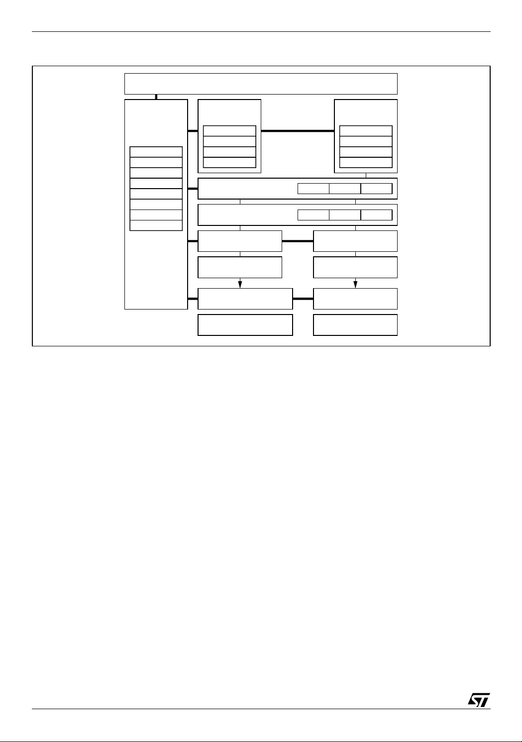
6 SOFTWARE ARCHITECTURE
The software is organized in 5 clusters:
– User interface API
– System services
– Network services
– TCP/IP socket
– ATM encapsulation
A description of the cluster contents is given in the software features section.
3/20
MTC50150
Figure 3. Embedded software block diagram
USER INTERFACE
SYSTEM
SERVICES
RTOS
MIB
CTRL-E
DOWNLOAD
FLASH MGR
ILMI
UNI3.1
DIAGNOSTIC
D02TL535
NETWORK
SERVICES
HTTP SRV
SNMP
TFTP
DNS
IP SOCKET
ATM ENCAPSULATION
AAL5/SAR
UTOPIA MASTER DRIVER
BRIDGE FIRMWARE
TCP UDP UDP
PPPoE PPPoA PPTPRAS
BRIDGING, SPANNING
ROUTER
RIP1.2
FIREWALL
NAT
DHCP
LEARNING TREE
MAC
MII DRIVER
ROUTER ADD-ON
7 SOFTWARE FEATURES
7.1 User Interface API
A development kit dedicated to the p latform allows acc ess through the API to specific code sections to
allow software customiz atio n. The dev el opm ent ki t prov ide s sou rce c od e for a p ac ket pho ne ap pli c ati on,
drivers and diagnostic software. Other stacks are delivered in the object code. A specific development environment is provided . It includes projec t profiling, managi ng, C compiler/ass embler and tools as well a
source level debugger.
7.2 System Services
MAPI offers an easy interface to control the operations necessary to setup the ADSL link and monitor the
operation conditions . The so ftware provides an o ptimiz ed con trol sequ ence to insure op timum op erati on
of the DynaMiTe™ chip set.
MIB2: RFC 1213: Management Information Bases (MIB2) is implemented in the device.
RTOS: Implemented RTOS is Posix compliant. The user can access various parts of the software blocks
through specific APIs. Alternate RTOS are planned.
Flash Initialization. Software is stored on an external Flash. At boot-up, the stored software is downloaded
to the device. By using co mpilation opti ons, software c an be executed fr om the internal RA M (intensive
operations) or executed from the flash. Execution is optimized by the use of an intermediate cache memory.
Startup initialization: Optional software images can be selected at startup of the device.
Broad Support Program: A BSP layer is provided to allow easy porting of proprietary software on the SOC
architecture. The BSP provides a unique hardware abstraction layer model valid for the entire product line.
This approach allows reuse of the custom solfware through the entire MTC-50xxx product line(*).
(*) starting with MTC-50150
4/20

MTC50150
7.3 Network Services
7.3.1 ILMI
Embedded software provides an I LMI 4.0 im plementatio n which han dles address registration (switch to
end device) and noti fication (end device to swi tch) as well as auto-confi guration. IL MI uses SNMP o ver
AAL-5 for transport.
7.3.2 UNI Signaling
Stackware includes support for standard ATM UNI signaling standards, including UNI 3.1.
7.3.3 RIP1/RIP2 IP Router
IP router software pr ovides implementations o f RIP 1 a nd RIP 2. The IP router is an I Pv4 r ou ter. Su ppor t
for new station discovery is provided.
7.4 TCP/IP Socket
7.4.1 TCP
Transport Control Protocol (TCP) is accessed using a standard socket interface to allow easy integration
of existing Layer 3 and higher software into the basic protocol stack.
7.4.2 IP
Internal protocol: IP a nd IP r outin g are both p art of the net work la ye r (layer 3). I P is ac tually r esp onsible
for delivering packets for which the router defines the direction.
7.4.3 DHCP RFC 2131, 2132
Dynamic Host Control Protocol (DHCP) provides both client & server functions. The client is typically used
to obtain an IP address from an ISP. The DHCP server is used to assign local IP client devices with designated IP addresse s. T he serv er lends addres ses for a li mited time. NAT reg isters loc al termi nal IP addresses and maintai ns a translation table to allow se nding and receiv ing data on the pu blic network b y
sharing only the residential gateway assigned public IP address.
7.4.4 NAT: RFC1631, 2663
The Network Address Tran slator (NAT) impleme nts Network and Port Ad dress Translation (NAT /PAT).
NAT allows a single public IP address on the WAN side to be sha red among m any dev ices on th e LAN
side. Combined with a DHCP serv er local devices are ass igned a private addre ss, hidden to the public
internet and changed frequently. The combination of DHCP and NAT provides a powerful isolation barrier
to external assault. NAT PAT features a number of AGL.
7.5 ATM Encapsulation and spanning-tree
RFC 1483/2684 provides a simple robust method of connecting end stations over an ATM network. User
data in the form of Ethernet packets are enca psulated into AAL-5 PDUs for transport over ATM. RF C
1483/2684 provides no AAA function (authentication, authorization & accounting).
7.5.1 Spanning-tree bridge (802.1d)
Bridge module provides a transparent bridge between two physically disjoint networks with spanning-tree
option. The spanning-tree algorithm handles redundancy and also increases robustness. It provides high
performance as well as flexibility to group interfaces for example to bridge the WAN only to LAN interfaces
but not to other WAN interfaces.
The ATM driver passes data between applicat ion software task s on the processor and a physical AAL5
hardware block.
5/20

MTC50150
7.6 Session Control
7.6.1 PPPoA (RFC 2364)
PPP over ATM provides on the CPE side a termination agent for the transportation for IP packets over an
ATM segment. A PPP session is established between the CPE and the central office (DSLAM). PPP provides AAA function (a uthentication, authorizatio n and accounting). The PPP packets enc apsulated according to RFC 2364 for transmission over an ATM segment. On the CPE side, the IP data can be
delivered to the end user over such technologies as Ethernet.
7.6.2 PPPoE (RFC 2516)
The PPP over Ethernet encap sulation is used to tr ansport Ether net PPP traffi c. The traffic is the n transported over the ATM link by encapsulating traffic using RFC1483/2683. There may be multiple PPP sessions, each termin ated i n th e IA D c lien t de vi ce . P PPoE r el ay agent works as a enhan ce d l ay er 2 brid ge.
It determines that wh ich locally origina ted PPPoE traffic be longs. The relay agent fo rwards that traffic,
without any unnecess ary processin g, only to the correct desti nation. Simi larly, rece ived data is i mmediately relayed only to the appropriate LAN client.
8 DEVELOPMENT ENVIRONMENT
The MTC5015 0 presents a comp rehensive set of software featu res. To allow ma nufacturer s to further customize the system, a s et of A PI func tions ar e mad e avail able. Th is us e of th e API fun ction s re quires the
acquisition of a deve lopment envir onment. T he develop ment environ ment is based on the following elements:
■ -ARM Developer Suite (ADS) v1.1
■ -ATI Development license
■ -ATI EDE (Embedded Development Environment)
■ -MS Developer Studio (VC++) v6.0 or higher
Along with the deve lop ment e nvironm ent a numbe r of tools a re prov ided to allo w th e dia gnostic and the
downloading operation of the executable on the nonvolatile memory of the MTC50150.
9 NOMINAL CHARACTERISTICS
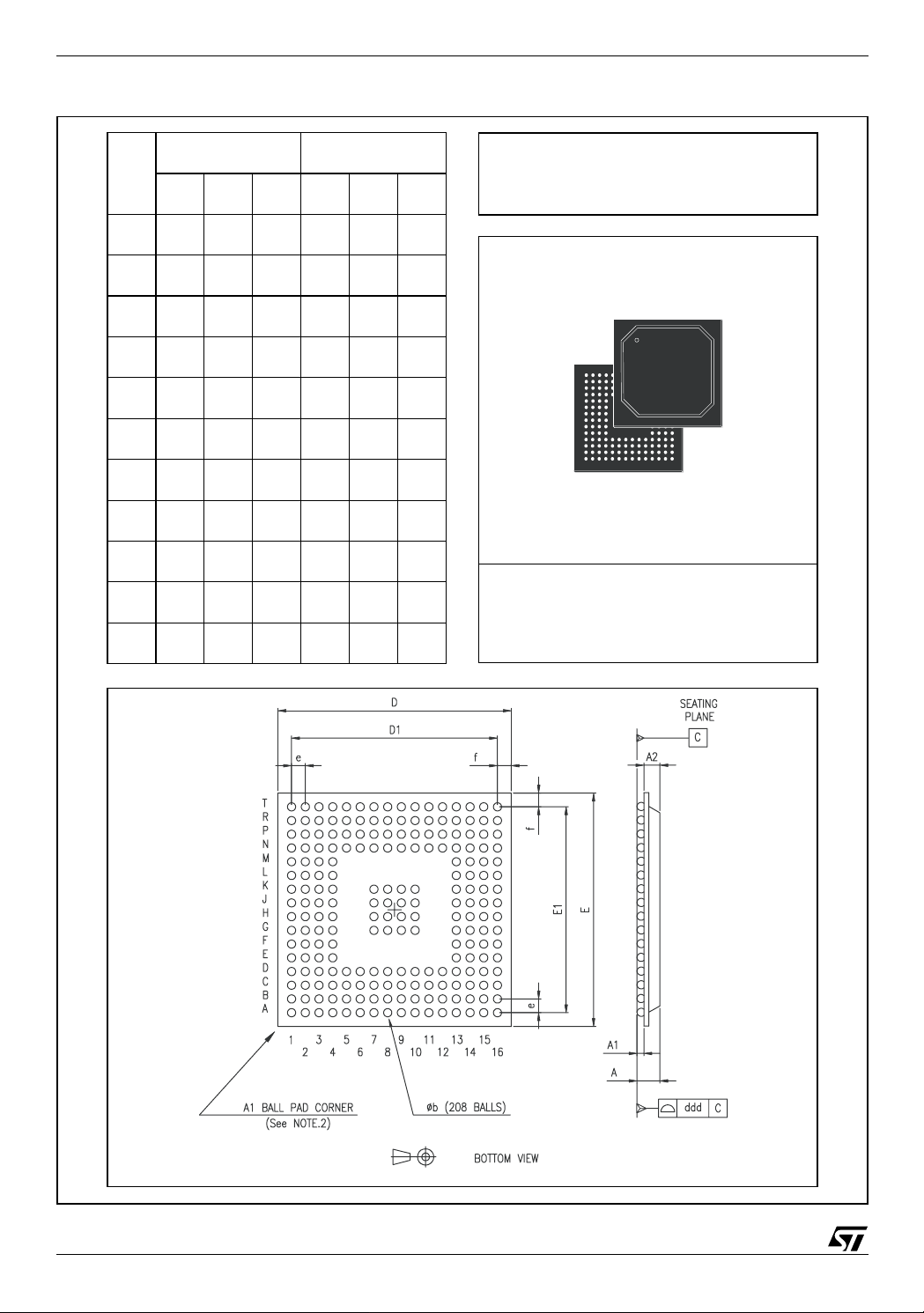
The MTC50150 processor is available in a 208-pin PBGA ( plastic ball grid arra y) package. All I/Os are
3.3V CMOS levels, with all inputs and 3-states having 5V tolerance. Supply voltages are 1.8 and 3.3V. No
pins have internal pull-ups and pull-downs.
Supply – Typical power supply voltage 1.8V
– Typical pad power supp ly vo ltag e 3.3 V
Threshold – Input low voltage -0.5V -1.0V
– Input high voltage 2.3V- 5.5V
Consumption – Core consumption: 1000mW, reduced power mode avail-
able.
Environment – Ambient temperature: 0C - 70C (32F - 158F)
– Industrial grade: -40C - 85C. (-49F - 185F)
Package – 208-pin plastic BGA packa ge
Techno logy – CMOS 0.18 micron
6/20

MTC50150
10 APPLICATION EXAMPLE
The example below show s the reference design developed for the ev aluation board. It is a complete
ADSL-based data gateway th at conne cts to th e ADSL en abled ph one jack an d provid es a con nection to
a 10/100bT Ethernet port. It utilizes a set of two ASSP available from ST.
The MTC50150 kit is composed of the following elements: A DynaMiTe™ ADSL modem and AFE
(MTC20174). Additional components are SDRAM and Flash memory and Ethernet PHY. Discrete components and connect or s are n ot shown on the block dia gr am. La rg er SDRAM and Flash can be c onn ec ted
to the MTC50150 to store and execute additional (custom) application.
Figure 4. Application block diagram
WAN LAN
ADSL
AFE
MTC50150
ETHERNET
PHY
MTC20174
SDRAM
Intensive qualification efforts have been spent on this reference design insuring users of the platform maximum interoperabili ty and smooth, rapid d esign-in, hence redu cing engineering effort and Total Time to
Market (TTM).
FLASH
D02TL544MOD1
7/20

MTC50150
11 MTC50150 PIN LIST
11.1 PIN DESCRIPTION
The pin list comprises of all functional and power supply pins.
A TBGA-208 package (TB208A) is used.
(I = Input, ID = Input with internal Pull-Down, IU= Input with internal Pull-Up, O = Output, B = Bidirectional,
OD = Open Drain, I/O D = Bidirec tiona l with Open Dr ain ou tput, O Z = Hi gh-Z Outp ut, P = Powe r Suppl y,
FS = Full Scan, NA = not available as pin).
Table 2. MTC50150 Pin list
Name Pin B Buffer Type Description
SDRAM Interface ( 57)
SD_nRAS N2 O PRT08DGZ SDRAM Row Address Strobe
SD_CLK P2 B PRB08DGZ SDRAM Clock
SD_nCAS N1 O PRT08DGZ SDRAM Column Address Strobe
SD_nWE N3 O PRT08DGZ SDRAM Write Strobe
SD_D31 R8 B PRB08DGZ SDRAM Data Bit 31
SD_D30 T8 B PRB08DGZ SDRAM Data Bit 30
SD_D29 P8 B PRB08DGZ SDRAM Data Bit 29
SD_D28 N8 B PRB08DGZ SDRAM Data Bit 28
SD_D27 T9 B PRB08DGZ SDRAM Data Bit 27
SD_D26 R9 B PRB08DGZ SDRAM Data Bit 26
SD_D25 N10 B PRB08DGZ SDRAM Data Bit 25
SD_D24 P10 B PRB08DGZ SDRAM Data Bit 24
SD_D23 T10 B PRB08DGZ SDRAM Data Bit 23
SD_D22 T11 B PRB08DGZ SDRAM Data Bit 22
SD_D21 R11 B PRB08DGZ SDRAM Data Bit 21
SD_D20 N12 B PRB08DGZ SDRAM Data Bit 20
SD_D19 P12 B PRB08DGZ SDRAM Data Bit 19
SD_D18 T12 B PRB08DGZ SDRAM Data Bit 18
SD_D17 R12 B PRB08DGZ SDRAM Data Bit 17
SD_D16 P13 B PRB08DGZ SDRAM Data Bit 16
SD_A0 T7 O PRT08DGZ SDRAM Address Bit 00
SD_A1 N6 O PRT08DGZ SDRAM Address Bit 01
SD_A2 P6 O PRT08DGZ SDRAM Address Bit 02
SD_A3 T6 O PRT08DGZ SDRAM Address Bit 03
8/20

Table 2. MTC50150 Pin list (continued)
Name Pin B Buffer Type Description
SD_A4 R6 O PRT08DGZ SDRAM Address Bit 04
SD_A5 T5 O PRT08DGZ SDRAM Address Bit 05
SD_A6 R5 O PRT08DGZ SDRAM Address Bit 06
SD_A7 N4 O PRT08DGZ SDRAM Address Bit 07
SD_A8 T4 O PRT08DGZ SDRAM Address Bit 08
SD_A9 P4 O PRT08DGZ SDRAM Address Bit 09
SD_A10 R4 O PRT08DGZ SDRAM Address Bit 10
SD_A11 T3 O PRT08DGZ SDRAM Address Bit 11
SD_A12 R3 O PRT08DGZ SDRAM Address Bit 12
SD_A13 T2 O PRT08DGZ SDRAM Address Bit 13
SD_A14 T1 O PRT08DGZ SDRAM Address Bit 14
SD_D15 G1 B PRB08DGZ SDRAM Data Bit 15
MTC50150
SD_D14 G3 B PRB08DGZ SDRAM Data Bit 14
SD_D13 G4 B PRB08DGZ SDRAM Data Bit 13
SD_D12 H2 B PRB08DGZ SDRAM Data Bit 12
SD_D11 H1 B PRB08DGZ SDRAM Data Bit 11
SD_D10 H3 B PRB08DGZ SDRAM Data Bit 10
SD_D9 H4 B PRB08DGZ SDRAM Data Bit 09
SD_D8 J4 B PRB08DGZ SDRAM Data Bit 08
SD_D7 J2 B PRB08DGZ SDRAM Data Bit 07
SD_D6 K4 B PRB08DGZ SDRAM Data Bit 06
SD_D5 K3 B PRB08DGZ SDRAM Data Bit 05
SD_D4 K1 B PRB08DGZ SDRAM Data Bit 04
SD_D3 L4 B PRB08DGZ SDRAM Data Bit 03
SD_D2 L3 B PRB08DGZ SDRAM Data Bit 02
SD_D1 L1 B PRB08DGZ SDRAM Data Bit 01
SD_D0 L2 B PRB08DGZ SDRAM Data Bit 00
SD_nCS P1 O PRT08DGZ SDRAM Chip Select
SD_CKE R1 O PRT08DGZ SDRAM Clock Enable
SD_DQM0 M1 O PRT08DGZ SDRAM Data Mask 0 (Byte Enable)
SD_DQM1 M2 O PRT08DGZ SDRAM Data Mask 1 (Byte Enable)
9/20

MTC50150
Table 2. MTC50150 Pin list (continued)
Name Pin B Buffer Type Description
SD_DQM2 P7 O PRT08DGZ SDRAM Data Mask 2 (Byte Enable)
SD_DQM3 N7 O PRT08DGZ SDRAM Data Mask 3 (Byte Enable)
ARM/Miscellane ou s Int erf ac e (4)
ARMDEBUG B7 I PDIDGZ ARM Debug Test mode (multiplexes the
ARM TAP onto the JTAG pins)
Tied to ‘0’ in functional mode
FLASHBOOT /
PLL_CTR_RUN
BYPASSPLL /
FS IN #15
UTOPIASEL R13 ID PDDWDGZ Select external Utopia Interface of ADSL
TCK E3 IU PDUWDGZ Boundary ScanTest Clock
TDI F3 IU PDUWDGZ Boundary Scan Test Data In
TDO E1 OZ PRT08DGZ Boundary Scan Test Data Out
TMS E4 IU PDUWDGZ Boundary Scan Test Mode Shift
NTRST F4 ID PDDWDGZ Boundary Scan Reset
ISA_nCS /
TRACEPORT9 /
U_NOTRXREF
A7 I PDIDGZ Boot from external Flash PROM rather
than from internal ROM
Starts/Stops the PLL test counter
Tied to ‘1’ in functional mode
C5 I /
I
JTAG/Te st Inte rf ace (5)
ISA-like Interface (42 )
H15 O PRT08DGZ ISA bus Chip Select / Address Enable /
PDIDGZ Bypass CPU clock generation PLL
Tied to ‘0’ in functional mode
Full scan input chain 15 (ARM946E)
core (Sachem_ip)
ETM9 Trace port 9 /
Utopia Receive Reference Clock
ISA_nRD B13 O PRT08DGZ ISA bus Read Strobe / Outp ut Enable
ISA_nWR C13 O PRT08DGZ ISA bus Wr ite Strobe
ROM_nCS A14 O PRT08DGZ Flash PROM Chip Select / Address
ROM_ADDR21 /
PLL_DIV_OUT/
TRACEPKT11 /
U_RXSOC
ROM_ADDR20 /
PLL_NOM_OUT /
TRACEPKT10 /
U_RXCLAV
ROM_ADDR19 /
TRACEPKT9 /
U_TXCLAV
10/20
D14 O /
O /
O /
OZ
E15 O /
O /
O /
OZ
E16 O /
O /
OZ
PRT08DGZ Flash PROM Address Bit 21 /
PRT08DGZ Flash PROM Address Bit 20 /
PRT08DGZ Flash PROM Address Bit 19 /
Enable
Divided clock in PLL test mode /
ETM9 Trace packet 11 /
Utopia Receive Start Of Cell
PLL output clock in PLL test mode/
ETM9 Trace packet 10 /
Utopia Receive Cell Available
ETM9 Trace packet 9 /
Utopia Transmit Cell Available

Table 2. MTC50150 Pin list (continued)
Name Pin B Buffer Type Description
MTC50150
ROM_ADDR18 /
TRACEPKT8
ROM_ADDR17 /
TRACEPKT7
ROM_ADDR16 /
TRACEPKT6
ROM_ADDR15 D13 O PRT08DGZ Flash PROM Address Bit 15
ROM_ADDR14 /
FS OUT #14
ROM_ADDR13 /
FS OUT #13
ROM_ADDR12 /
FS OUT #12
ROM_ADDR11 /
FS OUT #11
ROM_ADDR10 /
FS OUT #10
ROM_A DDR9 /
FS OUT #9
ROM_A DDR8 /
FS OUT #8
E14 O PRT08DGZ Flash PROM Address Bit 18 /
G14 O PRT08DGZ Flash PROM Address Bit 17 /
G13 O PRT08DGZ Flash PROM Address Bit 16 /
B12 O /
O
A12 O /
O
C12 O /
O
A11 O /
O
C11 O /
O
B10 O /
O
A10 O /
O
PRT08DGZ Flash PROM Address Bit 14
PRT08DGZ Flash PROM Address Bit 13
PRT08DGZ Flash PROM Address Bit 12
PRT08DGZ Flash PROM Address Bit 11
PRT08DGZ Flash PROM Address Bit 10
PRT08DGZ Flash PROM Address Bit 9
PRT08DGZ Flash PROM Address Bit 8
ETM9 Trace packet 8
ETM9 Trace packet 7
ETM9 Trace packet 6
Full scan output chain 14
Full scan output chain 13
Full scan output chain 12
Full scan output chain 11
Full scan output chain 10
Full scan output chain 9
Full scan output chain 8
ROM_A DDR7 /
FS OUT #7
ROM_A DDR6 /
FS OUT #6
ROM_A DDR5 /
FS OUT #5
ISA_ADDR4 /
ROM_ADDR4
ISA_ADDR3 /
ROM_A DDR3 /
FS IN # 3
ISA_ADDR2 /
ROM_A DDR2 /
TESTSEL106M
ISA_ADDR1 /
ROM_A DDR1 /
TESTSEL70M
ISA_ADDR0 /
ROM_A DDR0 /
FS IN # 6
C10 O /
O
D10 O /
O
A9 O /
O
B9 O PRB08DGZ ISA / Flash PROM Address Bit 4
C9 O /
O /
I
D9 O /
O /
I
D8 O /
O /
I
C8 O /
O /
I
PRT08DGZ Flash PROM Address Bit 7
Full scan output chain 7
PRT08DGZ Flash PROM Address Bit 6
Full scan output chain 6
PRT08DGZ Flash PROM Address Bit 5
Full scan output chain 5
PRB08DGZ ISA / Flash PROM Address Bit 3 /
Full scan input chain 3
PRB08DGZ ISA / Flash PROM Address Bit 2
Test clock select for PLL test mode
PRB08DGZ ISA / Flash PROM Address Bit 1
Test clock select for PLL test mode
PRB08DGZ ISA / Flash PROM Address Bit 0
Full scan input chain 6
11/20

MTC50150
Table 2. MTC50150 Pin list (continued)
Name Pin B Buffer Type Description
ISA_DATA15 /
ROM_ADDR23 /
PIPESTAT0 /
U_RXENB
ISA_DATA14 /
ROM_ADDR22/
TRACEPKT4 /
U_TXENB
ISA_DATA13 /
GPIO12 /
TRACEPKT2 /
U_RXADDR2
ISA_DATA12 /
GPIO11 /
TRACESYNC /
U_RXADDR1
ISA_DATA11 /
GPIO10 /
TRACEPKT3 /
U_RXADDR0
ISA_DATA10 /
GPIO9 /
TRACECLK /
U_TXADDR2
H13 B /
O /
O /
J13 B /
O /
O /
J14 B /
B /
O /
J16 B /
B /
O /
J15 B /
B /
O /
K13 B /
B /
O /
PRB08DGZ ISA / Flash PROM Data bus Bit 15 /
I
PRB08DGZ ISA / Flash PROM Data bus Bit 14 /
I
PRB08DGZ ISA / Flash PROM Data bus Bit 13 /
I
PRB08DGZ ISA / Flash PROM Data bus Bit 12 /
I
PRB08DGZ ISA / Flash PROM Data bus Bit 11 /
I
PRB08DGZ ISA / Flash PROM Data bus Bit 10 /
I
Flash PROM Address bit 23 in 8 bit
mode /
ETM9 Trace port Pipe status 0 /
Utopia Receive Enable
Flash PROM Address bit 22 in 8 bit
mode/
ETM9 Trace packet 4 /
Utopia Tran sm it En able
GPIO12 in 8 bit mode /
ETM9 Trace packet 2 /
Utopia Receive Address Bit 2
GPIO11 in 8 bit mode/
ETM9 Trace Sync signal /
Utopia Receive Address Bit 1
GPIO10 in 8 bit mode/
ETM9 Trace packet 3 /
Utopia Receive Address Bit 0
GPIO9 in 8 bit mode/
ETM9 Trace clock /
Utopia Transmit Address Bit 2
ISA_DATA9 /
GPIO8 /
TRACEPKT1 /
U_TXADDR1
ISA_DATA8 /
GPIO7 /
TRACEPKT0 /
U_TXADDR0
ISA_DATA7 /
FS IN #14
ISA_DATA6 /
FS IN #13
ISA_DATA5 /
FS IN #12
ISA_DATA4 /
FS IN #11
ISA_DATA3 /
FS IN #10
ISA_DATA2 /
FS IN #9
K14 B /
B /
O /
K16 B /
B /
O /
B14 B /
A15 B /
A16 B /
B16 B /
C15 B /
C16 B /
PRB08DGZ ISA / Flash PROM Data bus Bit 9 /
I
PRB08DGZ ISA / Flash PROM Data bus Bit 8 /
I
PRB08DGZ ISA / Flash PROM Data bus Bit 7
I
PRB08DGZ ISA / Flash PROM Data bus Bit 6
I
PRB08DGZ ISA / Flash PROM Data bus Bit 5
I
PRB08DGZ ISA / Flash PROM Data bus Bit 4
I
PRB08DGZ ISA / Flash PROM Data bus Bit 3
I
PRB08DGZ ISA / Flash PROM Data bus Bit 2
I
GPIO8 in 8 bit mode/
ETM9 Trace packet 1 /
Utopia Transmit Address Bit 1
GPIO7 in 8 bit mode/
ETM9 Trace packet 0 /
Utopia Transmit Address Bit 0
Full scan input chain 14
Full scan input chain 13
Full scan input chain 12
Full scan input chain 11
Full scan input chain 10
Full scan input chain 9
12/20

Table 2. MTC50150 Pin list (continued)
Name Pin B Buffer Type Description
MTC50150
ISA_DATA1 /
FS IN #8
ISA_DATA0 /
FS IN #7
AF_RXD3 /
FS IN #2
AF_RXD2 A1 I PDIDGZ ADSL AFE Receive Data Bit 2
AF_RXD1 A2 I PDIDGZ ADSL AFE Receive Data Bit 1
AF_RXD0 B3 I PDIDGZ ADSL AFE Receive Data Bit 0
AF_TXD3 /
FS OUT #4
AF_TXD2 /
FS OUT #3
AF_TXD1 /
FS OUT #2
AF_TXD0 /
FS OUT #1
AF_CLWD /
FS IN #1
D16 B /
D15 B /
B1 I /
E2 O /
O
D4 O /
O
D1 O /
O
D3 O /
O
C1 I /
I
PRB08DGZ ISA / Flash PROM Data bus Bit 1
PRB08DGZ ISA / Flash PROM Data bus Bit 0
I
ADSL Interface (13)
PDIDGZ ADSL AFE Receive Data Bit 3 /
I
PRT08DGZ ADSL AFE Transmit Data Bit 3 /
PRT08DGZ ADSL AFE Transmit Data Bit 2 /
PRT08DGZ ADSL AFE Transmit Data Bit 1 /
PRT08DGZ ADSL AFE Transmit Data Bit 0 /
PDIDGZ ADSL Start Of Word Indication /
I
Full scan input chain 8
Full scan input chain 7
Full scan input chain 2
Full scan output chain 4
Full scan output chain 3
Full scan output chain 2
Full scan output chain 1
Full scan input chain 1
AF_CTRLDATA /
FS OUT #15
MCLK B4 I PDISDGZ ADSL Master Clock
MnRST A3 I PDISDGZ ADSL Master (Chip) Reset
AF_nPOWERLOW /
FS OUT #16
M_TXCLK /
U_TXCLK
M_TXEN /
U_RXDATA4
M_TXD3 /
U_RXDATA3
M_TXD2 /
U_RXDATA2
M_TXD1 /
U_RXDATA1
M_TXD0 /
U_RXDATA0
C2 O /
O
D2 O /
O
Ethernet MII Interface (18)
P15 I PDISDGZ Ethernet MII Transmit Clock /
T14 O /
OZ
R14 O /
OZ
T15 O /
OZ
T16 O /
OZ
R16 O /
OZ
PRT08DGZ ADSL Serial Data Transmit Channel /
Full scan output chain 15 (A946E)
PRT08DGZ ADSL Power Down Analog FrontEnd /
Full scan output chain 16 (A946E)
Utopia Tran sm it Clo ck
PRT08DGZ Ethernet MII Transmit Enable /
Utopia Receive Data Bit 4
PRT08DGZ Ethernet MII Transmit Data Bit 3 /
Utopia Receive Data Bit 3
PRT08DGZ Ethernet MII Transmit Data Bit 2 /
Utopia Receive Data Bit 2
PRT08DGZ Ethernet MII Transmit Data Bit 1 /
Utopia Receive Data Bit 1
PRT08DGZ Ethernet MII Transmit Data Bit 0 /
Utopia Receive Data Bit 0
13/20

MTC50150
Table 2. MTC50150 Pin list (continued)
Name Pin B Buffer Type Description
M_TXER /
U_RXDATA5
M_CRS /
U_TXDATA7
M_COL /
U_TXDATA6 /
FS IN #4
M_RXCLK /
U_RXCLK
M_RXDV /
U_TXDATA4
M_RXD3 /
U_TXDATA3
M_RXD2 /
U_TXDATA2
M_RXD1 /
U_TXDATA1
M_RXD0 /
U_TXDATA0
M_RXER /
U_TXDATA5
T13 O /
OZ
M14 I PDIDGZ Ethernet MII Carrier Sense /
M13 ID /
I /
I
N15 I PDISDGZ Ethernet MII Receive Clock /
P16 I PDIDGZ Ethernet MII Receive Data Valid /
N14 I PDIDGZ Ethernet MII Receive Data Bit 3 /
N16 I PDIDGZ Ethernet MII Receive Data Bit 2 /
N13 I PDIDGZ Ethernet MII Receive Data Bit 1 /
M15 I PDIDGZ Ethernet MII Receive Data Bit 0 /
M16 I PDIDGZ Ethernet MII Receive Error /
PRT08DGZ Ethernet MII Transmit Error /
Utopia Receive Data Bit 5
Utopia Transmit Data Bit 7
PDDWDGZ Ethernet MII Collision Detection /
Utopia Transmit Data Bit 6 /
Full scan input chain 4
Utopia Receive Clock
Utopia Transmit Data Bit 4
Utopia Transmit Data Bit 3
Utopia Transmit Data Bit 2
Utopia Transmit Data Bit 1
Utopia Transmit Data Bit 0
Utopia Transmit Data Bit 5
M_MDC /
U_RXDATA6
M_MDIO /
U_RXDATA7 /
FS IN #5
GPIO6 /
SER2SI /
PIPESTAT2 /
U_RXADDR3
GPIO5 /
SER2SO /
PIPESTAT1 /
U_RXADDR4
GPIO4 /
M_LINK /
TRACEPKT15 /
U_TXSOC
GPIO3 /
PB1 /
TRACEPKT14 /
U_TXADDR3
L14 O /
OZ
L13 B /
OZ /
H16 B /
I /
O /
H14 B /
O /
O /
F16 B /
I /
O /
F14 B /
O /
O /
I
GPIO Interface (7)
I
I
I
I
PRT08DGZ E the rnet MII Manageme nt Da ta Clo ck /
Utopia Receive Data Bit 6
PRB08DGZ Ethe rnet MII Manageme nt Da ta /
Utopia Receive Data Bit 7 /
Full scan input chain 5
PRB08DGZ General Purpose Pin 6 /
CleanDMEP Serial Interface 2 – serial
input /
ETM9 Trace port Pipe status 2 /
Utopia Receive Address Bit 3
PRB08DGZ General Purpose Pin 5 /
CleanDMEP Serial Interface 2 – serial
output /
ETM9 Trace port Pipe status 1 /
Utopia Receive Address Bit 4
PRB08DGZ General Purpose Pin 4 /
Ethernet Link Status Input /
ETM9 Trace packet 15 /
Utopia Transmit Start Of Cell
PRB08DGZ General Purpose Pin 3 /
Main Clock Control PB1 /
ETM9 Trace packet 14 /
Utopia Transmit Address Bit 3
14/20

Table 2. MTC50150 Pin list (continued)
Name Pin B Buffer Type Description
MTC50150
GPIO2 /
PB0 /
FS IN #16
GPIO1 /
SI_RCLK /
SER2nCTS /
TRACEPKT13 /
U_TXADDR4
GPIO0 /
SER2nRTS /
TRACEPKT12 /
U_NOTTXREF
SI_SIN /
SER1SI
SI_SOUT /
SER1SO
SI_nRTS /
SER1nRTS
SI_nCTS /
SER1nCTS
A13 B /
O /
I
F13 B /
I /
I /
O /
I
G16 B /
O /
O /
I
SI Serial Interface (4)
C7 I PDIDGZ Serial Interface Serial Data Input /
B8 O PRT08DGZ Serial Interface Serial Data Output /
A8 O PRT08DGZ Serial Interface Not Ready To Send /
D7 I PDIDGZ Serial Interface Not Clear To Send /
PRB08DGZ General Purpose Pin 2 /
Main Clock Control PB0 /
Full scan input chain 16 (A946ES)
PRB08DGZ General Purpose Pin 1 /
External UART Clock /
CleanDMEP Serial Interface 2 nCTS
/ ETM9 Trace packet 13 /
Utopia Transmit Address Bit 4
PRB08DGZ General Purpose Pin 0 /
CleanDMEP Serial Interface 2 nRTS
/ ETM9 Trace packet 12 /
Utopia Transmit Reference Clock
CleanDMEP Serial Interface 1 – serial
input
CleanDMEP Serial Interface 1 – serial
output
CleanDMEP Serial Interface 1 nRTS
CleanDMEP Serial Interface 1 nCTS
Miscellaneous Test Pins (2)
IDDQMode C6 I PDIDGZ IDDQ mode activation
FSSHIFT A6 ID PDDWDGZ Full Scan Sh ift En able
Core Power Supply Pins (26) [1.8V]
VDD_CORE F2,
K2,
R2,
P5,
N9,
R10,
R15,
L15,
E13,
B15,
D12,
B6,
B2
P PVDD1DGZ 1.8V
15/20

MTC50150
Table 2. MTC50150 Pin list (continued)
Name Pin B Buffer Type Description
VSS_CORE F1,
N5,
P9,
K10,
L16,
F15,
G10,
B11,
D5,
G9,
H9,
J10,
H10
VDD_IO C3,
G2,
J3,
M3,
P3,
R7,
N11,
P14,
K15,
G15,
C14,
D11,
D6
P PVSS3DGZ 0 V, comm on with VS S_ IO
I/O Power Supply Pins (28) [3.3V]
P PVDD2DGZ 3.3 V
VSS_IO H8,
H7,
J1,
M4,
K7,
K8,
P11,
J9,
G8,
G7,
J7,
J8,
K9
PLL Digital and Analog Power Supply Pins (4) [1.8V]
VDD_DIG_PLL A5 P PVDD1P 1.8V (DVDD)
VSS_DIG_PLL B5 P PVSS1P 0 V (not common with VSS_CORE)
VDD_AN_PLL A4 P PVDD1P 1.8V (AVDD)
VSS_AN_PLL C4 P PVSS1P 0 V (not common with VSS_CORE)
Unconnected Pads (0) (all have an internal pull-down resistor)
SWMODE0 - NA PDDWDGZ do not bond; ‘0’ default value, bond to
P PVSS3DGZ 0 V, comm on with VS S_ CO R E
(DVSS)
(AVSS)
nearby VDD_IO to get ‘1’ value
16/20

Table 2. MTC50150 Pin list (continued)
Name Pin B Buffer Type Description
MTC50150
SELECT106M - NA PDDWDGZ do not bond; ‘0’ default value, bond to
SELECT70M - NA PDDWDGZ do not bond; ‘0’ default value, bond to
SELRSTDLY - NA PDDWDGZ do not bond; ‘0’ default value; bond to
nearby VDD_IO to get ‘1’ value
(activates 106 MHz CPU clock)
nearby VDD_IO to get ‘1’ value
(activates 70 MHz CPU clock)
nearby VDD_IO to get ‘1’ value
(activates prolonged external reset
delay)
Summary of functional, power supply, and unconnected Pins:
Table 3. Summary of MTC50150 Pin list
Pin Group Pin Number
SDRAM 57
ARM/Misc 4
JTAG test port 5
Flash PROM / ISA like interface 42
ADSL Front End 13
Ethernet MII 18
GPIO 7
Serial Interface 4
Test pins 2
I/O supply 26
Core supply 26
PLL analog + digital supply 4
Not Connected 0
Total (TBGA-208) 208
17/20
MTC50150
Figure 5. PBGA208 (17x17x1.97mm) Mechanical Data & Package Dimensions
mm inch
DIM.
MIN. TYP. MAX. MIN. TYP. MAX.
A 1.970 0.077
A1 0.270 0.011
A2 1.470 0.058
b 0.450 0.500 0.550 0.018 0.020 0.022
D 16.80 17.00 17.20 0.661 0.669 0.677
D1 15.00 0.590
E 16.80 17.00 17.20 0.661 0.669 0.677
E1 15.00 0.590
e 0.950 1.000 1.050 0.037 0.039 0.041
f 0.875 1.000 1.125 0.034 0,039 0.044
ddd 0.200 0.008
OUTLINE AND
MECHANICAL DA T A
PBGA 208
(17x17x1.97)
18/20
7196686 A

Table 4. Revision History
Date Revision Description of Chan g es
September 2004 1 First Issue in EDOCS dms.
MTC50150
19/20

MTC50150
Information furnished is believed to be accurate and reliable. However, STMicroelectronics assumes no responsibility for the consequences
of use of such information nor for any infri ngement of patents or other rights of third parties which may result from its use. No licens e is granted
by implication or otherwise under any patent or patent rights of STMicroelectronics. Specifications mentioned in this publication are subject
to change without no tice. This publication supersedes and replaces all information previously supplied. STMicroelectronics pro d uc ts are not
authorized for use as critical components in life support devices or systems without express writt en approval of STMicroelectronics.
The ST logo is a registered trademark of STMicroelectronics.
All other names are the property of their respective owners
© 2004 STMicroelectronics - All rights reserved
Australia - Belgium - Brazil - Canada - China - Czec h Republic - Finland - France - Germany - Hong Kong - India - Is rael - Italy - Japan -
Malaysia - Malta - Morocco - Singapore - Spain - Sweden - Switzerland - United Kingdom - United States of America
STMicroelectronics group of companies
www.st.com
20/20
 Loading...